EFFECTS OF SURFACE MODIFICATION ON
CHARGE-CARRIER DYNAMICS AT SEMICONDUCTOR INTERFACES
Thesis by Agnes Juang
In Partial Fulfillment of the Requirements for the Degree of Doctor of Philosophy
California Institute of Technology Pasadena, California
2003
Acknowledgments
The past five years have been the most incredible time of my life. Graduate school has changed the way I learn, the way I think, and the way I see things. I have gained so much more than what I had anticipated throughout the course of my study at Caltech, and I am glad that I chose to come here and stayed even when things got tough. Along the way, many people have landed their helping hands and gave me the strength to hang on. Without them, this thesis would not have been born.
I am grateful to have had a chance to learn electrochemistry first hand from Prof. Nathan Lewis. He is not only an exceptional scientist, but also one of the best in the field. I have learned a lot from Nate over the years including his high standard for research and persistent scientific honesty; his scientific intuition has not ceased to amaze me. I truly appreciate his forbearance and trust for allowing me to become an
independent researcher.
to finish up on time, and I have to thank them for that. I am also very thankful to have a great collaborator Oren Scherman for the work included in Chapter 4. He saved me from having to do many organic synthesis, and I could always count on him for the best home-made chemicals.
Although Caltech is a wonderful place to be for researchers, it can sometimes make individuals feel trapped or isolated. Without my two closest friends at Caltech, Heather Cox and Dr. Anne Fu, and the almost-weekly lunch meetings we had, I would not have had many chances to talk about something other than science and politics when I am on campus. I also thank all of Nate’s administrative assistants, especially Nannette Pettis, who had offered me help and an open door for small chats and complaints. Many people in Chemistry Department and Caltech administrative offices had also made my life easier when I was the head TA for Chem 1, and for that I gratefully thank them.
Best of all, I have met someone who understands not only my research, but also my heart. I thank Nick for his caring, patience, and love. He has shown me the true meaning of partnership through his constant support and understanding. He has also brought endless joy and laughter into my life; with him, life is always fun, fun, fun!
Abstract
Understanding the basic concepts of semiconductor junctions is an important step towards the development of efficient solar energy conversion devices. The work
described in this dissertation includes both the investigation of semiconductor/liquid junctions and the modification of semiconductor surfaces for achieving chemical control over physical properties.
The interfacial charge-carrier dynamics of n-GaAs/CH3CN junctions has been investigated. Differential capacitance barrier height measurements and steady-state current density–potential (J–E) measurements were used to evaluate the degree of partial Fermi-level pinning. The presence of irreversible chemical and/or electrochemical changes on n-GaAs electrodes immersed in CH3CN-CoCp2+/0
solutions was examined using x-ray photoelectron spectroscopy (XPS) and cyclic voltammetric studies that were designed to probe surface reactions.
Chemical modifications of semiconductor surfaces can provide a reliable mean to control physical properties of semiconductor interfaces. The growth of robust polymer films that are covalently attached to Si surfaces via a Si-C linkage was demonstrated. Uniform polymer overlayers of different thicknessess were formed using a general method combining chlorination/Grignard reaction with ring-opening metathesis
polymerization (ROMP). The surfaces of these modified Si were characterized by x-ray photoelectron spectroscopy (XPS), scanning electron microscopy (SEM), ellipsometry, and/or profilometry. The charge-carrier dynamics at these modified Si/air interfaces was investigated using transient photoconductivity decay method. Time-dependent
Table of Contents
Acknowledgments...iii
Abstract... v
Table of Contents ... vi
List of Figures... ix
List of Tables ... xii
Chapter 1 Introduction ... 1
1. Overview... 2
2. Charge-Transfer Equilibration at Semiconductor Heterojunctions... 5
3. Current–Voltage Properties of a Semiconductor Diode ... 12
4. Charge-Carrier Recombination Mechanisms... 14
4.1. Interfacial Electron Transfer/Thermionic Emission... 17
4.2. Electron Tunneling ... 18
4.3. Surface-State Recombination... 19
4.4. Depletion-Region Recombination... 23
4.5. Bulk-Region Recombination ... 24
5. Surface States ... 26
6. References ... 28
Chapter 2 Photoelectrochemical Behavior of n-GaAs in
Acetonitrile Solutions ... 29
1. Introduction ... 30
2. Background ... 32
2.1. Determination of the Electron-Transfer Rate Constant at the Semiconductor/Liquid Interface... 32
2.2. Fermi-Level Pinning... 34
3. Experimental ... 37
3.1. Electrode Material and Etching... 37
3.2. Solvents and Reagents ... 38
3.3. Electrochemical Measurements ... 39
3.3.1. Impedance Measurements ... 39
3.3.2. Steady-State Current Density vs. Potential Characteristics... 41
3.4. Surface Analysis of n-GaAs in Contact with CH3CN-CoCp2+/0 Solution... 44
3.4.1. X-ray Photoelectron Spectroscopy... 44
4. Results... 46
4.1. Differential Capacitance vs. Potential Results and the Barrier Height of n-GaAs/CH3CN-CoCp2+/0 Contacts... 46
4.2. Steady-State J–E Behavior of n-GaAs/CH3CN-CoCp2 +/0 Contacts... 55
4.2.1. J–E Data for n-GaAs electrodes in CH3CN-CoCp2 +/0 solutions ... 55
4.2.2. Photoresponses of n-GaAs electrodes in CH3CN-CoCp2+/0 and CH3CN-Fc2+/0 solutions ... 55
4.2.3. Effects of Exposure to CH3CN-CoCp2+/0 Solutions on the Behavior of n-GaAs/CH3CN-Fc +/0 Contacts... 56
4.3. X-Ray Photoelectron Spectroscopy and Cyclic Voltammetry Data of n-GaAs Surfaces in Contact with the CH3CN-CoCp2+/0 Electrolyte ... 62
5. Discussions... 66
5.1. Electrochemical Properties of n-GaAs/CH3CN Contacts... 66
5.2. Interfacial Rate Constant Determinations Using n-GaAs/CH3CN Contacts ... 67
6. Summary ... 70
7. Acknowledgments ... 70
8. References and Notes ... 71
Chapter 3
Fabrication and Characterization of n-Si(111)
Based Metal-Insulator-Semiconductor Diodes ... 74
1. Introduction ... 75
2. Experimental ... 80
2.1. Solvents and Reagents ... 80
2.2. Semiconductor Material and Etching ... 81
2.3. Surface Modification ... 82
2.4. Metal Deposition and Device Fabrications... 85
2.4.1. The First-Generation MIS Device... 85
2.4.2. The Second-Generation MIS Device ... 86
2.4.3. The Third-Generation MIS Device ... 86
2.4.4. The Fourth-Generation MIS Device ... 87
2.5. Surface Characterization... 93
2.6. Electrical Measurements... 94
3. Results... 97
3.1. Surface Modification ... 97
3.2. The J–E Behaviors of MIS Diodes ... 100
4. Discussions... 107
5. Summary ... 110
Chapter 4
Transient Photoconductivity Decay Measurements
of Polymer-Terminated Silicon Surfaces ... 113
1. Introduction ... 114
2. Experimental ... 119
2.1. Chemicals... 119
2.2. Preparation of Substrates ... 120
2.3. Surface Modification ... 121
2.3.1. Chlorination ... 121
2.3.2. Terminal-Olefin Addition via Grignard Reaction... 122
2.3.3. Catalyst Addition ... 123
2.3.4. Polymerization ... 123
2.4. Surface Characterizations ... 124
2.4.1. X-ray Photoelectron Spectroscopy... 124
2.4.2. Overlayer Thickness Measurements: Ellipsometry and Profilometry ... 125
2.4.3. Scanning Electron Microscopy ... 126
2.5. Photoconductivity Decay Measurements ... 130
3. Results... 138
3.1. Surface Modifications ... 138
3.1.1. Polynorbornene-Terminated Si... 139
3.1.2. PolyDCPD-Terminated Si ... 139
3.1.3. ROMP of COD and COT ... 140
3.1.4. Control Experiments ... 140
3.2. Surface Characterizations ... 148
3.2.1. Polymer Thickness Measurements... 148
3.2.2. Scanning Electron Microscopy ... 148
3.3. Photoconductivity Decay Measurements ... 156
3.3.1. C3 Olefin-Terminated and C3 Olefin-Polymer-Terminated Si Surfaces ... 156
3.3.2. Effects of Olefin Linker Chain Length... 158
3.3.3. C5 Olefin-Terminated and C5 Olefin-Polymer-Terminated Si Surfaces ... 158
3.4. Time-Dependent XPS Studies: Oxidation of Modified Si surfaces in Air... 172
4. Discussions... 180
4.1. Surface Modifications and Characterizations ... 180
4.2. Surface Recombination Velocity and Oxidation ... 184
5. Summary ... 188
6. Acknowledgments ... 188
List of Figures
Chapter 1
Figure 1.1 A band bending diagram for an ideal n-type semiconductor/liquid
junction... 8 Figure 1.2 A band bending diagram for an ideal n-type semiconductor/metal
junction... 10 Figure 1.3 Various types of recombination pathways for an n-type
semiconductor/liquid junction. ... 16 Figure 1.4 A schematic depicting the microscopic balance between electron
and hole capture and emission processes at recombination centers
in the semiconductor. ... 22
Chapter 2
Figure 2.1 Opecircuit photovoltage vs. equilibrium cell potential for the n-GaAs/CH3CN-LiClO4 system at Jph = 1.0 mA cm-2
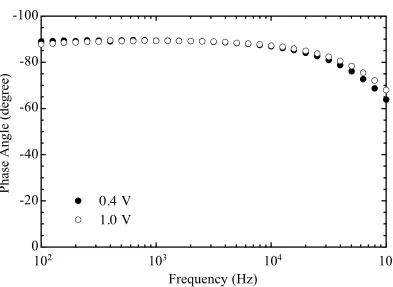
. ... 36 Figure 2.2 Circuit diagrams for a semiconductor/liquid junction. ... 43 Figure 2.3 (a) A representative Bode plot for the n-GaAs/CH3CN-CoCp2
+/0
junction... 49 (b) A plot of phase angle vs. log f for the n-GaAs/CH3CN-CoCp2+/0
junction... 50 (c) A representative Nyquist plot for the n-GaAs/CH3CN-CoCp2
+/0
junction... 51 Figure 2.4 (a) Mott-Schottky plot of the n-GaAs/CH3CN-CoCp2+/0
junction. ... 53 (b) Linear extrapolations of the Mott-Schottky data shown in (a). ... 54 Figure 2.5 Representative J–E behaviors of n-GaAs electrodes in contact with
CH3CN-CoCp2+/0
solution. ... 57 Figure 2.6 Representative J–E behaviors of n-GaAs electrodes in contact with
slightly wet CH3CN-CoCp2+/0
solution... 58 Figure 2.7 (a) The J–E behavior of n-GaAs electrode in contact with CH3
CN-Fc+/0
solution. ... 60 (b) The J–E behavior of n-GaAs electrode in contact with
CH3CN-Fc+/0
solution after performing J–E scans in CH3CN-CoCp2+/0
solution. ... 61 Figure 2.8 XP survey spectra of n-GaAs before and after 10 minutes of J–E
scans in a CH3CN-CoCp2 +/0
solution. ... 64 Figure 2.9 Cyclic voltammogram of n-GaAs in CH3CN-0.7 M LiClO4 in the
Chapter 3
Figure 3.1 A band bending diagram of a metal/insulator-semiconductor (MIS)
junction... 79
Figure 3.2 An illustration of the first-generation MIS device... 89
Figure 3.3 An illustration of the second-generation MIS device. ... 90
Figure 3.4 An illustration of the third-generation MIS device... 91
Figure 3.5 An illustration of the fourth-generation MIS device... 92
Figure 3.6 XP survey spectra of H-terminated, Cl-terminated, C3-terminated, C6-terminated, and C10-terminated Si... 98
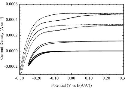
Figure 3.7 (a) J–E behavior of H-terminated Si in contact with 450 Å of Ni... 102
(b) J–E behavior of C3-terminated Si in contact with 450 Å of Ni... 102
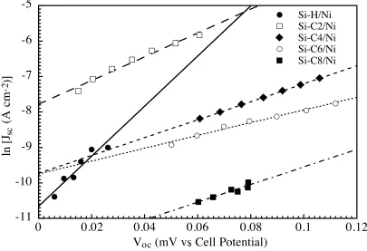
Figure 3.8 J–E behaviors of a series of CnH2n+1-terminated Si/Ni (n = 2, 4, 6, and 8) and an H-terminated Si/Ni junctions in the dark... 104
Figure 3.9 Photoresponses of a series of CnH2n+1-terminated Si/Ni (n = 2, 4, 6, and 8) and an H-terminated Si/Ni junctions in the dark... 105
Figure 3.10 Time-dependent J–E behaviors of a C8H17-terminated Si/Ni junction in the dark ... 106
Chapter 4 Figure 4.1 Polymer-terminated Si surfaces reported in literature ... 117
Figure 4.2 Experimental approach to produce a variety of covalently attached polymer overlayers on Si surfaces ... 127
Figure 4.3 A schematic of the radio frequency (rf) apparatus used to perform photoconductivity decay measurements... 133
Figure 4.4 (a) A schematic of the controlled-environment chamber for sample storage ... 136
(b) A photograph of the controlled-environment setup... 137
(c) A detailed photograph of the chamber interior... 137
Figure 4.5 XP survey spectra of each step of the surface modification... 142
Figure 4.6 XP survey spectra of polyDCPD-terminated Si. ... 144
Figure 4.7 XP survey spectra of control experiments... 146
Figure 4.8 (a) A partial profilometric surface profile of a polynorbornene-terminated Si surface... 151
(b) A SEM image of the same surface at 30¥ magnification ... 151
Figure 4.9 SEM top-view images of polynorbornene-terminated Si surfaces. ... 153
Figure 4.10 A cross-sectional SEM image of a polynorbornene-covered Si surface ... 155
Figure 4.12 Time dependence of the mean carrier lifetimes for C3 terminated, C3 polynorbornene-terminated, and C3
olefin-polyDCPD-terminated Si in air ... 162 Figure 4.13 Time dependence of the mean carrier lifetimes for mixed
methyl/C3 terminated, C3 terminated, C5
olefin-terminated, and C6 olefin-terminated Si surfaces in air... 163 Figure 4.14 Time-resolved photoconductivity decay curves of C5
terminated, C5 polynorbornene-terminated, and C5
olefin-polyDCPD-terminated Si surfaces in an N2(g) ambient... 164 Figure 4.15 (a) Time dependence of the mean carrier lifetimes for C5
olefin-terminated Si surfaces exposed to high temperature/humidity and
low temperature/humidity conditions ... 166 (b)Time dependence of the mean carrier lifetimes for C5
olefin-polynorbornene-terminated Si surfaces exposed to high
temperature/humidity and low temperature/humidity conditions... 167 (c) Time dependence of the mean carrier lifetimes for C5
olefin-polyDCPD-terminated Si surfaces exposed to high
temperature/humidity and low temperature/humidity conditions... 168 Figure 4.16 Time dependence of the mean carrier lifetimes for C5
terminated, C5 polynorbornene-terminated, and C5 olefin-polyDCPD-terminated Si surfaces exposed to a low
temperature/humidity condition... 169 Figure 4.17 Time dependence of the mean carrier lifetimes for C5
terminated, C5 polynorbornene-terminated, and C5 olefin-polyDCPD-terminated Si surfaces exposed to a high
temperature/humidity condition... 170 Figure 4.18 Time-dependent high-resolution XP spectra of C5
olefin-terminated Si under low temperature/humidity condition... 174 Figure 4.19 Time-dependent high-resolution XP spectra of C5
olefin-terminated Si under high temperature/humidity condition... 175 Figure 4.20 Time-dependent high-resolution XP spectra of C5
olefin-polyDCPD-terminated Si under low temperature/humidity
condition ... 176 Figure 4.21 Time-dependent High-resolution XP spectra of C5
olefin-polyDCPD-terminated Si under high temperature/humidity
condition ... 177 Figure 4.22 Time-dependent high-resolution XP spectra of H-terminated Si
under low temperature/humidity condition ... 178 Figure 4.23 A space-filling model of a Ru catalyst and a Si surface... 183 Figure 4.24 The aged Si 2p high-resolution XP spectra of H-TERMINATED,
C5 olefin-terminated, and C5 olefin-polyDCPD-terminated
List of Tables
Chapter 3
Table 3.1 A summary of reaction time, overlayer thickness, and air stability
of alkyl-terminated Si... 84
Chapter 4
Table 4.1 List of reagents and reaction conditions for Si surface modification ... 129 Table 4.2 Dependence of the polymer overlayer thickness on the
concentration of norbornene in the solution ... 150 Table 4.3 Time-dependent measured carrier recombination lifetimes and
surface recombination velocities for various modified Si surfaces ... 171 Table 4.4 Time dependence of the silicon oxide growth for
Chapter 1
1.
Overview
From supporting our everyday lives to promoting cutting-edge technological advancements, fossil fuels have played a very important role for our civilization. As the finite amount of fossil reserves are being depleted at a rate that will not sustain the continuing growing human population, the need for affordable alternative energy sources has become more prominent. Renewable energy sources, like wind, hydro, and solar powers, are abundant and can be harnessed and utilized without further polluting our green planet. However, the well-established infrastructure for the extraction and distribution of fossil fuel-derived power has allowed the cost to remain relatively low, making more expensive solar energy less attractive. As people start to recognize our unsustainable practice of energy consumption, many may soon start to incorporate solar energy as part of their primary power source. For the prevalent utilization of solar energy to become a reality in a near future, scientists have to develop more efficient solar energy conversion devices while lowering the costs at the same time. Understanding the basic concepts of semiconductor junctions is the first step towards this goal.
The plants have evolved to make extensive use of solar energy in photosynthesis to convert sun light directly into stored fuels. Typical photosynthetic process, however, convert only 3–5% of the total incident solar power into fuel storage,1
yet is sufficient to sustain life on Earth. On the other hand, the conversion of photon energy into electrical energy has been realized in photovoltaic devices consisting of two different solids connected at an abrupt junction which has the ability to direct electrical current flow in one direction through the external circuit.2
durable,3
with such small economic value, the wide implementation of photovoltaic devices is proved to be difficult. A less-expansive solar energy conversion can be achieved by photoelectrochemical cells, which involve the use of semiconductor to adsorb incident light and the electrochemical process at semiconductor/liquid junction to allow energy conversion. The photoelectrochemical cells can be constructed to produce electricity or to store chemical fuels, and the efficiencies are generally between those of photovoltaics and photosynthesis.1
The basic challenge in developing practical photoelectrochemical solar energy conversion devices is the trade-off between the semiconductor stability and conversion efficiency.1
Semiconductors with relatively high bandgap energies, such as titanium dioxide (TiO2), absorb high-energy photons but only a small portion of the solar spectrum. TiO2 is stable in aqueous solutions, but suffers a poor solar-conversion
efficiency of about 1%. Materials made of germanium have very small bandgaps that can absorb a large fraction of the solar spectrum; unfortunately, a significant amount of absorbed energy is wasted as heat when the highly excited electrons readily relax to the energy of the conduction band edge. Semiconductors with moderate bandgaps, such as silicon (Si), gallium arsenide (GaAs), and indium phosphide (InP), are unstable in aqueous solutions, but prove to be the most efficient due to a well-overlapped bandgap energies with terrestrial solar spectrum.
combination is often toxic and not yet suitable for the commercial use, the
semiconductor/non-aqueous liquid contacts are ideal for scientific investigation due to the constructional simplicity. Understanding of photoelectrochemical processes at these junctions is viable for future improvements of solar energy conversion devices.
This thesis includes investigations of charge-carrier dynamics at semiconductor junctions through the effects of surface modifications. A brief introduction to the fundamental theory of semiconductor heterojunctions and charge-carrier recombination process is included in this chapter. Chapter 2 presents both electrochemical and surface investigations of n-GaAs/CH3CN interfaces. It also addresses the very importance of understanding the charge-carrier recombination mechanism in correctly assessing the electron-transfer processes across a semiconductor/liquid junctions. Chapter 3 describes an attempt to fabricate metal-insulator-semiconductor (MIS) diodes for improved
2.
Charge-Transfer Equilibration at Semiconductor Heterojunctions
1,4When a semiconductor comes into contact with a liquid or a metal phase, the difference in the electrochemical potential of the semiconductor and the contacting phase results in charge equilibration at the heterojunction. Since works present in this thesis involve n-GaAs and n-Si, the ideal junction between an n-type semiconductor and a contacting phase with a more positive electrochemical potential is described. The electrochemical potential of a freestanding semiconductor is set by the position of its Fermi level (EF), which is the energy level where the probability of finding an electron is one-half. When a solution containing a redox couple A/A–
(A is an electroactive acceptor and A–
is a donor) is the contacting phase, the electrochemical potential of the contacting phase (EF,c) is E(A/A
–
) and is given by the Nernst equation:
E(A / A–)=E∞¢(A / A–) (+ kT)ln([ ] / [A A–]) (1.1)
where Eû´(A/A–
) is the electrochemical potential of the redox couple A/A– under standard-state conditions, k is the Boltzmann’s constant, and T is the absolute
temperature. When the contacting phase is a metal the EF,c is EF,m. Since it is difficult to experimentally determine the value of EF,m, work function of the metal (jm) is often used instead of EF,m.
When two phases are brought into contact, electrons flow from the phase with more negative initial electrochemical potential to the other, in this case from the
semiconductor to the contacting phase, until the electrochemical potentials of both phases are in equilibrium. As the result of this charge-transfer process, both the semiconductor and the contacting phase lose their original charge neutrality. Excess positive charges are produced in the semiconductor while an excess of negative charges appears in the
even with dilute concentration of redox species, or the metal far exceeds the number in a semiconductor, the accepted negative charges do not change the position of the EF,c. On the other hand, the Fermi level of the semiconductor becomes more positive, and the equilibrium position of the Fermi level for both phases is essentially equal to the initial value of the EF,c.
During the equilibration process, electrons that are the most easily ionized are removed first. This means that the charges are removed from dopant atoms before Si atoms are ionized. Since a certain number of electrons are needed from the
semiconductor in order to reach the charge-transfer equilibrium, usually more than an atomic layer of dopant atoms are ionized. The distance into the semiconductor from the interface that is required for removal of charges from all the dopant atoms within this region is called the depletion width (W), and the region is called depletion region. A more positive initial EF,c or a more negative initial EF requires more layers of dopant atoms to be ionized, hence a larger W. The charge-transfer equilibration causes electric fields and electric potential gradients to rise in both phases, and the presence of this electric field at the interface is essential for the effective charge separation at
semiconductor/liquid junction to separate charge effectively. A band bending diagram is used to depict the potential energy vs. distance relationship for a semiconductor/liquid junction (Figure 1.1) and for a semiconductor/metal junction (Figure 1.2). The electric potential energy levels of both conduction band (Ecb) and valence band (Evb) drop within the depletion width as moving away from the interface and into the bulk of
semiconductor. A barrier height (fb) is thus formed at the interface, and the barrier height energy (qfb) is defined as the differences between the equilibrium Fermi level and the energy of the conduction band edge. In the case of semiconductor/metal junction, the fb can be calculated using thermodynamic model:5,6
Figure 1.1
A band bending diagram for an ideal n-type semiconductor/liquid junction before equilibrium (a) and at equilibrium (b). (a) Before charge-transfer equilibration occurs, the energy levels of the conduction and the valence bands of the semiconductor are the same everywhere from the surface to the bulk. When a semiconductor with a more negative Fermi level (EF) is brought into contact with a solution with a redox potential E(A/A–
), electrons flow from the semiconductor to the solution phase. (b) After charge-transfer equilibration has occurred, a depletion layer of a width W formed in the
semiconductor, and the contact potential drops primarily across this region. The Fermi level is the same across the junction at all points. The parameter qVn is defined as the difference between EF and Ecb in the bulk, Vbi is the built-in voltage of the junction, and the barrier height (fb) is defined as fb = Vbi + Vn, and qfb is the difference between Ecb at the interface and E(A/A–
Energy (eV)
(+)
(–)
E
(A/A
- )
Semiconductor
Solution
(b)
W
q
f
bqV
bi
E
FE
cbE
vbqV
n
x=0
x=W
E
(A/A
- )
(a)
Semiconductor
Solution
e–
E
FE
cbE
vbqV
n
Figure 1.2
Energy (eV)
(+)
(–)
E
F,mj
mc
sE
FE
cbE
vbW
q
f
bqV
bi
E
vacuumMetal
Semiconductor
E
F,m(b)
x=0
x=W
j
mc
sE
FE
cbE
vbE
vacuumMetal
Semiconductor
(a)
e–
3.
Current–Voltage Properties of a Semiconductor Diode
When a semiconducting material is illuminated with photons of sufficient energy (≥ bandgap energy, Eg), electrons are excited from valence band orbitals to the
conduction band and leave behind positively charged sites (commonly referred to as “holes”). In the absence of an electric field, these photoexcited electrons quickly relax to their ground states and recombine with the holes. With the presence of an electric field formed at the semiconductor heterojunction, photogenerated carriers can be separated since electrons have a tendency to move away from the more negative interface while holes move towards it. The photogenerated electrons can then be collected at the ohmic back contact and directed through the external circuit to do useful work. The separation of charge carriers at semiconductor/liquid and semiconductor/metal junctions is the basis of solar energy conversion by photoelectrochemical cells and photovoltaics.
The flow of electrons through the external circuit due to photoexcitation is
measured as the photocurrent (Jph). The current can also flow in the opposite direction of the Jph due to recombination of electron-hole pairs, and this unfavorable current is called reserve saturation current or recombination current (J0). The discussion of charge-carrier recombination mechanisms is also in order. The total current (J) flowing across an n-type semiconductor heterojunction is described by the diode equation:3,7
J J J qV
kT
= - Ê
-ËÁ ˆ¯˜ -È
Î
Í ù
û ú
ph 0 exp 1
g (1.3)
maximum Gibbs free energy available from the cell. For Jph >> J0, equation 1.3 can be rearranged to yield
V kT
q J
J oc
ph
= Ê
ËÁ ˆ ¯˜
g ln
0
(1.4)
4.
Charge-Carrier Recombination Mechanisms
10Once the electron-hole pairs are generated in the semiconductor by
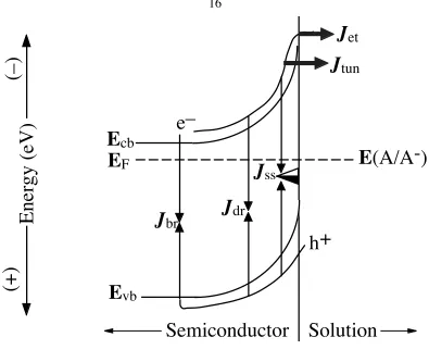
photoexcitation, electrons and holes can find ways to recombine before being harnessed to do useful work. Generally there are five types of recombination mechanisms that can contribute to the recombination current (J0). Depending on the location of recombination relative to the junction, the recombination pathways are grouped into either majority carrier processes or minority carrier processes. Figure 1.3 depicts several pathways that the recombination processes can occur at the semiconductor/liquid junction. All possible recombination mechanisms usually occur simultaneously for a given sample, and the total recombination current is the sum of the individual recombination currents:
J0 = Jet +Jtun +Jss+Jdr+Jbr (1.5)
where subscript “et” is the recombination due to interfacial electron transfer when the contacting phase is a liquid and is replaced by “th”, the thermionic emission, when the contacting phase is a metal, subscript “tun” is the recombination due to electron tunneling, subscript “ss” is the surface-state recombination, subscript “dr” is the depletion-region recombination, and subscript “br” is the bulk-region recombination. Depending on the semiconductor dopant density (Nd), barrier height, the density of surface traps located within the bandgap, and the applied bias (V), one pathway usually dominates the recombination event and therefore J0. These recombination processes will be discussed briefly in the next two sections.
Energy (eV)
(+)
(–)
Semiconductor Solution
e–
h+
E
(A/A-)
E
F
E
cb
E
vb
J
br
J
dr
J
ss
[image:28.612.126.521.58.391.2]J
et
J
tun
Figure 1.3
Various types of recombination pathways for an n-type semiconductor/liquid junction. The Jet is the current caused by electron transfer over the potential barrier from the semiconductor to the redox acceptors in the solution. The Jtun describes the majority carrier tunneling current through the potential barrier. Recombination due to the surface states near the interface results in Jss, while recombination in the depletion and bulk regions produces Jdr and Jbr, respectively. Both Jet and Jtun are currents requiring injection of majority carriers from the semiconductor, hence majority carrier recombination
4.1. Interfacial Electron Transfer/Thermionic Emission
At semiconductor/metal junctions (Schottky junctions), the interfacial electron transfer over the top of the surface barrier is called thermionic emission. Since the metal has a very high density of unoccupied levels, every electron that reaches the top of the surface barrier is assumed to be captured by the metal phase.7,9
The relationship between J0 and fb can be described by the thermionic emission theory:
11
J A T q
kT b 0 =
-Ê
Ë ˆ¯
* * 2exp f (1.6)
where A** is the modified Richardson constant, which is the probability of an electron being injected into the metal once it reaches the interface. Since fb is not a function of Nd, the thermionic emission current is independent of the dopant density of
semiconductor. When the thermionic emission is the dominant recombination mechanism, the experimentally determined g is 1, and the activation energy is qfb.
At semiconductor/liquid junctions, the interfacial electron-transfer event is governed by both the concentration of electrons at the semiconductor surface (ns) and the concentration of acceptor species in solution ([A]). The recombination current can be expressed as:12,13
J0 =qk n Aet s[ ] (1.7)
4.2. Electron Tunneling
The electron tunneling rate can be calculated with quantum theory by modeling the potential barrier as triangular. The probability of tunneling through the base of the barrier is
Ttun =exp{-8pW[2qme*(|Vbi |+V)]1 3/ /3h (1.8)
where me* is the effective mass of an electron, Vbi is the difference between the
conduction band edge at the surface and in the bulk, and h is the Planck’s constant. The total current can be described as
J=qnth tunT ( )E dn( )E (1.9)
The rate of electron tunneling through the potential barrier usually only dominates the recombination rate when the semiconductor is highly doped. When the dopant
4.3. Surface-State Recombination
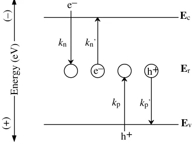
Nonradiative recombination mediated by energy levels within the bandgap can be described by Shockley-Read-Hall (SRH) statistics.14,15
The rate of surface-state
recombination can be derived by evaluating the microscopic balance between electrons and holes capture and emission processes by recombination centers at the semiconductor surface.
Assuming a given number density of recombination centers at surface (Nr,s, cm -2
) exist at an energy within the bandgap Er,s (Figure 1.4). The net rate of electron occupying these recombination centers is equal to the capture rate of electrons in conduction band minus the thermal emission rate of electrons back to the conduction band:
d N f
dt n k N f k N f
( )
( )
r,s r,s
s n,s r,s r,s n,s r,s r,s
= 1- - ¢ (1.10)
and the net rate of holes in valence band occupying these recombination centers is
d N f
dt p k N f k N f
[ ( )]
( )
r,s r,s
s p,s r,s r,s p,s r,s r,s 1
1
- =
- ¢ - (1.11)
¢ = - =
kn,s k Nn,s cexp[(Er,s Ec,s) /kT] k nn,s 1,s (1.12)
¢ = - =
kp,s k Np,s vexp[(Er,s Ev,s) /kT] k pp,s 1,s (1.13)
Nc and Nv are the density of electronic states in the conduction band and valence band, and Ec,s and Ev,s are the energy of the conduction and valence band edges at the surface, respectively.
Under the steady-state conditions, the occupancy density of the states is constant, and the recombination rate (Us) is equal to d(Nr,sfr,s)/dt = d[Nr,s(1-fr,s)]/dt. The fr,s can be solved by setting equations 1.10 and 1.11 equal to each other. Substituting the expression for fr,s back into either equation and realizing n1,sp1,s = ni
2
(ni is the intrinsic carrier concentration) yields
U N k k n p n
k n n k p p
s r,s
n,s p,s s s i 2
n,s s 1,s p,s s 1,s
=
-+ + +
( )
( ) ( ) (1.14)
Equation 1.14 represent sthe net rate of surface-state recombination for recombination centers located at a single energy level Er,s, and the total surface-state recombination current can be obtained by integrating Us over all possible recombination center energies. Surface recombination velocity (S) represents the pseudo-first-order rate constant for surface-state recombination of minority carrier and is commonly used to characterize the surface property of semiconductors. During photoexcitation, the surface carrier concentrations can be described as the sum of equilibrium and injected carrier concentrations (ns = n0,s + Dns and ps = p0,s + Dps). Substituting these terms and Us ∫ SDps into equation 1.14 results in the following expression, taking into account that n0,sp0,s = ni
2 :
S N k k n p n p n
k n n n k p p p
= + +
+ + + + +
r,s
n,s p,s 0,s 0,s s s s n,s 0,s s 1,s p,s 0,s s 1,s
[ ( / ) ]
( ) ( )
D D D
Since S (has units of velocity, cm s-1
) is a function of electron and hole
concentrations, the parameter depends on variables such as illumination level, applied potential, and temperature. At high level injection, concentrations of photogenerated carriers Dns and Dps are much greater than n0,s and p0,s, respectively, and Dns = Dps. Equation 1.13 can be rewritten as:
S N k k
k k
=
+
r,s
n,s p,s n,s p,s
(1.16)
At low level injection, Dns = Dps, Dps >> p0,s, and Dns << n0,s; equation 1.13 can then be simplified:
S=N kr,s p,s =1 /tp,s (1.17)
where tp,s is defined as minority carrier lifetime at the surface. When S is measured under either of these conditions, S is independent of carrier concentrations and allows for the extraction of surface recombination trap density without the effect of perturbation. At high level injection the slowest of either electron or hole capture dominates the S, while it is controlled only by the hole capture at low level injection. The surface-state
recombination current can be expressed in a way similar to a diode equation by factoring out the injected carrier concentration Dps:
J=qU=qSp0,s[exp(-qV kT/ )-1] (1.18)
Energy (eV)
(+)
(–)
h+
e–
e–
h+
E
r
E
c
E
v
k
p
k
n
k
n’
[image:34.612.130.517.112.407.2]k
p’
Figure 1.4
4.4. Depletion-Region Recombination
Depletion-region recombination can also be calculated using SRH statistics. We use the Equation 1.14 derived in the previous section, and drop the subscript “s” in all parameters to yield the following expression, with Nr (having a unit of cm
-3 ) now accounts for the density of recombination centers within the semiconductor:
U N k k np n
k n n k p p
=
-+ + +
r
n p i
2
n 1 p 1
( )
( ) ( ) (1.19)
Since only those recombination centers with energy levels at the mid-gap are the most effective traps, we can assume kn = kp. To obtain the depletion-region recombination current, U has to be integrated over the limits of depletion region. The value of U has a large dependence on both n and p, and the maximum value of U exist when n = p.
Umax ni qV kT p
=
-2t exp( /2 ) (1.20)
The integral ÚU(x)dx can then be replaced by the Umax multiplied by a width over which this maximum rate occurs. The effective width for the integration is kTW/q(Vbi+V), and the depletion-region recombination current can be obtained:
J qUdx kTWn
V V qV kT
kTW q V V
= =
+
-+
Ú
0 2 2/ ( )
( )exp( / )
bi i
p bi
t (1.21)
From equation 1.21, a g of 2 is often an indication that the recombination current is dominated by the depletion-region recombination. Assuming Jdr dominates the recombination current, substituting ni = (NcNv)
1/2
J kTW N N
V V kT qV kT
0
c v p bi
g
=
+ -
-( )
( ) exp( / )exp( / )
2t E 2 2 (1.22)
4.5. Bulk-Region Recombination
The current for the bulk recombination process is a function of hole diffusion rate into the bulk region of the semiconductor. Assuming that depletion-region recombination does not occur, and at any point x, the recombination rate in the bulk is the same as the diffusion rate:
[ ( )p x p x( )] / D p x( ) x
- 0 tp + pd =
d
2
2 0 (1.23)
where p(x) and p0(x) are the hole concentration and the equilibrium hole concentration at a point x in the bulk, and Dp is the hole diffusion coefficient. Since the total current at steady state is the same everywhere in the bulk, the total bulk recombination current can be determined by solving the hole concentration at the deletion layer edge. Two
boundary conditions will be applied. First is the assumption of the absence of depletion-region recombination at the depletion layer edge x = W:
n W p W( ) ( )=ni2exp(-qV kT/ ) (1.24)
Because the injected minority carrier concentration is much lower than the dopant density, n(W) ª n(W), and equation 1.24 becomes
p W( )= p0exp(-qV kT/ ) (1.25)
p x( )= p0+ p0[exp(-qV kT/ )-1]exp[ (- -x W) /Lp) (1.26)
where Lp is the hole diffusion length. Substituting this expression into Jp = qD[dp(x)/dx], and then the current at x = W can be evaluated:
J W qD p
L qV kT
p
p 0 p
( )= [exp(- / )-1] (1.27)
If the bulk-region recombination is the dominant mechanism, the g is expected to be 1, and the activation energy Eg. If Jp(W) is equal to the total bulk recombination current:
J qD p
L
qD n L N 0
p 0 p
p i 2
p d
5.
Surface States
10In order to improve the efficiency and the stability of photoelectrochemical or photovoltaic devices, the unfavorable current due to recombination has to be suppressed. While many strategies to improve the solar energy conversion devices have been
researched by others, the central theme of this thesis is to approach the challenge by investigating the surface states at the semiconductor/liquid junction and proposing a solution to improve the stability by surface modification. As the size of semiconductor devices continues to decrease, the effects of surface defects also become considerably more significant. Understanding of semiconductor surface properties and developments of methods that can improve the electrical properties of semiconductors can certainly provide unimaginable benefits for technologies of the future.
The different orbital structure of a semiconductor surface compared to its bulk usually results in one or more energy levels located inside of the bandgap region. These localized surface states can be either intrinsic or extrinsic in nature. The intrinsic surface states can arise because the surface atoms of a semiconductor do not have the periodic bonding structure that exists in the crystal lattice, or due to the reconstruction of the surface. The extrinsic surface states are the result of interface formation. Surface defects can emerge if a reaction or bonding occurs between the two phases in contact, and the adsorption or attachment of chemical impurities can also contribute to the surface states.
works presented in Chapters 3 and 4 involve surface modification of Si and the effects on the solid-state junction behaviors. Surface modification can be one of the easiest
6.
References
(1) Tan, M. X.; Laibinis, P. E.; Nguyen, S. T.; Kesselman, J. M.; Stanton, C. E.; Lewis, N. S. Prog. Inorg. Chem. 1994, 41, 21.
(2) Chapin, D. M.; Fuller, C. S.; Pearson, G. L. J. Appl. Phys. 1954, 25, 676.
(3) Fahrenbruch, A. L.; Bube, R. H. Fundamentals of Solar Cells: Photovoltaic Solar Energy Conversion; Academic: New York, 1983.
(4) Kumar, A.; Wilisch, W. C. A.; Lewis, N. S. CRC Critical Rev.1993, 18, 327. (5) Rhoderick, E. H.; Williams, R. H. Metal-Semiconductor Contacts; 2nd ed.;
Oxford University Press: New York, 1988.
(6) Sharma, B. L., Ed. Metal-Semiconductor Schottky Barrier Junctions and Their Applications; Plenum: New York, 1984.
(7) Sze, S. M. The Physics of Semiconductor Devices; 2nd ed.; Wiley: New York, 1981.
(8) Weast, R. C.; Astle, M. J.; Bayer, W. H. Handbook of Chemistry and Physics; 71st ed.; CRC Press: Boca Baton, FL., 1991.
(9) Fonash, S. J. Solar Cell Device Physics; Academic: New York, 1981.
(10) Lewis, N. S.; Rosenbluth, M. In Photocatalysis: Fundamentals and Applications; Serpone, N., Pelizzetti, E., Eds.; John Wiley & Sons: New York, 1989, pp 45. (11) Crowell, C. R.; Sze, S. M. Solid State Elec. 1966, 9, 1035.
(12) Memming, R. In Electroanalytical Chemistry; Bard, A. J., Ed.; Marcel Dekker, Inc.: New York, 1979; Vol. 11, p 1.
(13) Gerischer, H. In Physical Chemistry: An Advanced Treatise; Eyring, H., Henderson, D., Yost, W., Eds.; Academic: New York, 1970; Vol. 9A, pp 463. (14) Shockley, W.; Read, W. T. Phys. Rev. 1952, 87, 835.
Chapter 2
1.
Introduction
The photoelectrochemical behavior of GaAs/liquid contacts has attracted much
attention in attempts to compare theoretical predictions with the experimental behavior of
semiconductor electrodes.1-16
There has been significant controversy regarding the
electron-transfer rate constant, ket, at semiconductor/liquid interfaces. While many
experimental results and theoretical studies have indicated that the upper bounds on ket is
on the order of 10–17
to 10–16
cm4
s–1
,4,9-11,15-17
other reports have suggested that ket can be as
large as 10–12
to 10–10
cm4
s–1
.7,18-20
Steady-state current density (J) vs. potential (E) data
obtained on n-GaAs/CH3CN-cobaltocenium-cobaltocene (CoCp2) +/0
contacts in the limit
where the observed rate does not exhibit the expected second-order rate law (first order in
the surface electron concentration and first order in the redox acceptor concentration)
have been interpreted to indicate that ket values at semiconductor/liquid contacts can be as
high as 10–10
cm4
s–1
.7
Subsequent reports on n-GaAs/CH3CN contacts have relied upon
solvent-suspended quartz crystal microbalance measurements to indicate that both
cobaltocene and cobaltocenium adsorb onto the GaAs surface.8
Assumptions about the
effective electron-transfer distance to the adsorbed species, the distance-dependence of
the orbital coupling overlap, and the surface coverage of adsorbed electroactive species in
this system have then yielded a 10,000-fold reduction in the inferred ket value to ketª 10–14
cm4
s–1
.7,8
It is therefore of great interest and importance to examine in detail the J–E
properties of the n-GaAs/CH3CN interface. The behavior of n-GaAs in contact with
CH3CN has been studied previously by a number of workers. Wrighton and Bard used
cyclic voltammetry techniques to conclude that Fermi-level pinning was present at
n-GaAs/CH3CN contacts over a wide range of redox potentials. 21
Nagasubramanian,
measurements of n-GaAs/CH3CN contacts. 22
Other studies indicating non-ideal junction
behavior of n-GaAs electrodes in propylene carbonate, tetrahydrofuran,
dimethylformamide, and aluminum chloride-butylpyridinium chloride molten salt
electrolyte systems have been reported.23-31
Reduction of the influence of surface states
has, in certain cases, resulted in efficient GaAs-based photoelectrochemical cells,
specifically for n-GaAs/CH3CN-ferricenium-ferrocene (Fc +/0
) contacts.32,33
While J–E behaviors of n-GaAs/CH3CN contacts with a series of metallocenes
have been studied previously in our laboratory, the focus of this chapter involves the
investigation of the photoelectrochemical properties of n-GaAs/CH3
CN-colbaltocenium-cobaltocene (CoCp2
+/0
) contacts. The presence of Fermi-level pinning is confirmed by
correlating the barrier height obtained for this junction with prior results. This chapter
also presents a series of experiments designed to probe the presence of irreversible
chemical and/or electrochemical changes on GaAs electrodes during electrochemical
process in CH3CN-CoCp2 +/0
solution. These results display the non-ideal behavior of n
-GaAs/CH3CN-CoCp2
+/0
junction and consequently the invalidity of ket extraction using
2.
Background
2.1. Determination of the Electron-Transfer Rate Constant at the
Semiconductor/Liquid Interface
Current density vs. potential (J–E) measurements, in conjunction with kinetic
information obtained from impedance measurements, can be useful tools for assessing the
electron-transfer rate constants, ket at semiconductor/liquid interfaces. In order to extract
robust ket values from the steady-state J–E data, the following three conditions must be
satisfied.
(1) The electron transfer from the conduction band of a semiconductor to an outer
sphere redox acceptor in solution must follow a second-order rate law given by
-d =
dt k n
[ ]
[ A
A]
et s (2.1)
where ns is the concentration of surface electrons in the conduction band, and [A] is the
concentration of redox acceptors located near the surface of the semiconductor. The
interfacial flux must be shown to be first order in the ns at the semiconductor surface and
first order in the [A] in the solution.4,34
In this case, interfacial electron transfer
dominates the recombination current, and J0 = qketns[A]. By varying the concentration of
redox acceptors, Voc should change accordingly.
A prior study of n-GaAs/CH3CN-Fc +/0
contacts in our laboratory had shown that a
change of two orders of magnitude of [A] and [A–
], while the solution potential remained
constant, produced no change in Voc value at a constant light intensity. There was also no
change in Voc at a constant photocurrent density as [A] was increased from 0.5 mM to
33.4 mM while [A–
] remained constant.35
variation in [A] did not affect the interfacial flux, and therefore interfacial electron
transfer current does not dominate the recombination current.
(2) The semiconductor band edges do not move with changes in the concentration of
the redox acceptor species. Otherwise, the validation of the rate law is hindered when
both variables of the rate law, ns and [A], are simultaneously changed.
If the band edges stay at the same positions when the redox potential is varied,
then the barrier height of the junction, which is the difference between the semiconductor
conduction band edge and the solution redox potential, should change linearly with the
changes in the redox potential of the contacting solution. When this relationship is not
observed, the junction is Fermi-level pinned, and the band edges could shift with changes
in the cell potential. A prior investigation on Fermi-level pinning at n-GaAs/CH3CN
junctions was conducted by measuring the Voc values at different cell potentials,35
and is
presented in section 2.2 of this chapter. Although the relationship between the Voc and
the cell potential can provide an indication for the degree of Fermi-level pinning, the
observed changes in Voc could also be caused by reasons other than the band edge
movement. For example, the interfacial electron transfer current could increase with
changes in the equilibrium barrier height at the interface, or the surface-state
recombination current could have increased due to the changes in equilibrium occupation
fraction of the surface states. Since these conditions are capable of affecting the
measured Voc values as well, the barrier height measurement would be essential for
confirming the presence of Fermi-level pinning.
(3) The capture of the electrons by surface states does not compete kinetically with
the direct electron transfer from the semiconductor to the redox acceptor species.4,34,36-39
The surface states can either be intrinsic or arise from adsorption of the redox species. If
the semiconductor surface reacts with the contacting solution, it is a good indication that
The investigation of n-GaAs surface reaction in contact with CH3CN-CoCp2 +/0
is
one of the main focuses of this chapter. The Voc of this junction was larger than expected
at such a negative cell potential, which is fairly close to the GaAs conduction band edge.
If the GaAs surface is modified during the electrochemical operation in this solution, the
extraction of ket value from the steady-state J–E data of this junction would certainly not
be possible.
2.2. Fermi-Level Pinning
In an ideal situation, a change in the redox potential of the solution should result
in a defined change in the barrier height (fb) of the junction; however, this behavior is not
always observed experimentally. When a reliable barrier height measurement technique
was unavailable, open-circuit photovoltages, Voc, were measured and related to the
thermodynamic quantities for the investigation of the Fermi-level pinning. For an n-type
semiconductor when the interfacial electron transfer is the dominating recombination
process, Voc can be related to the build-in voltage (Vbi) according to the equation:
V kT
q
J
qN k A V
oc ph c et bi = Ê ËÁ ˆ ¯˜ + ln
[ ] (2.2)
However, if the interfacial electron transfer current is much less than the total
recombination current, then the inequality in Equation 2.2 must hold. Since fb = Vbi +
(kT/q)ln(Nc/Nd), Voc can be related to fb as follows:
V kT
q
J
qN k A
oc ph c et b < Ê ËÁ ˆ ¯˜ + ln
[ ] f (2.3)
The electrochemical behavior of a series of n-GaAs/CH3CN contacts has been
investigated over a significant range of Nernstian solution potentials, E(A/A–
ascertain whether “ideal” behavior of the Voc vs. E(A/A–
) is observed for these contacts,
or whether Fermi-level pinning, which would lead to apparent band edge shifts as
E(A/A–
) is changed,21
is present in these systems. The former condition is required for a
straightforward extraction of ket values from J–E data, while, in contrast, the latter
behavior has been observed in prior cyclic voltammetry and impedance measurements of
n-GaAs/CH3CN contacts. 22,40-42
Several different metallocene-based redox couples, spanning a wide range of
formal potentials, Eo'(A/A–
), were used to produce a variation in the Nernstian potentials
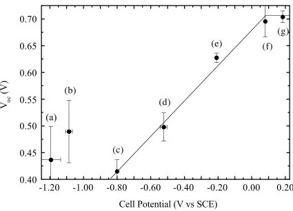
of the electrolyte solutions from –1.2 V to +0.2 V vs. SCE. Figure 2.1displays the Voc of
each system recorded at a light intensity sufficient to provide a photocurrent density of 1
mA cm–2
at each n-GaAs/CH3CN contact. Despite a change of over 1.2 V in E(A/A –
)
between the n-GaAs/CH3CN-Co(C5H4CH3)2 +/0
and the n-GaAs/CH3CN-Fc +/0
contacts, the
Voc only changed by ~0.3 V.43
In the ideal model of semiconductor
photoelectrochemistry, the Voc should be linearly dependent on E(A/A–
), with a slope
close to unity, for a homologous series of redox species. Instead, a much weaker
dependence of Voc was observed as E(A/A–
) was varied, and the presence of Fermi-level
pinning in this system over the range of potentials investigated was indicated.
Furthermore, for E(A/A–
) more negative than –0.80 V vs. SCE, the measured Voc values
that are larger than expected from the linear region signals the possibility of a chemical
reaction between the n-GaAs and CH3CN-based electrolyte under the conditions
0.40
0.45
0.50
0.55
0.60
0.65
0.70
-1.20
-1.00
-0.80
-0.60
-0.40
-0.20
0.00
0.20
V
oc(V)
Cell Potential (V vs SCE)
[image:48.612.112.537.122.428.2](b)
(a)
(c)
(d)
(e)
(f)
(g)
Figure 2.1Open-circuit photovoltage vs. equilibrium cell potential for the n-GaAs/CH3CN-LiClO4
system at Jph = 1.0 mA cm –2
. The redox couples used for this system are (a)
Co(C5H4CH3)2 +/0
, (b) CoCp2 +/0
, (c) [CoCp(C5H4CO2CH3)] +/0
, (d) Co(C5H4CO2CH3)2 +/0
, (e)
Fe[C5(CH3)5]2 +/0
, (f) Fe(C5H4CH3)2 +/0
, (g) FeCp2 +/0
3.
Experimental
3.1. Electrode Material and Etching
Single-crystal Si-doped (100)-oriented n-GaAs (Laser Diode Co.) with dopant
density, Nd, of (0.9–1.9) ¥ 1017
cm–3
and wafer thickness of 400–500 µm were used.
Ohmic contacts were prepared by thermal evaporation of a 1000 Å layer of 98% Au:2%
Ge alloy (Alfa Aesar) or 88% Au:12% Ge alloy (Aesar) on the unpolished side of the
wafers, followed by annealing in forming gas at 475 °C for 5 minutes.33
Electrodes were
fabricated by attaching a tinned copper wire (22 AWG, Belden) to the ohmic contact
using electrically conductive silver print (GC Electronics). The wire was encased in glass
tubing and the backside and edges of the electrode were sealed with insulating white
epoxy (Epoxy Patch Kit 1C, Dexter Corp.), leaving only the polished surface of the
crystal exposed. Electrode areas were determined by digitizing magnified scanned
images of the electrode along with a micro ruler using ImageSXM program. The typical
exposed electrode areas were 0.15–0.25 cm2
.
For surface x-ray photoelectron spectroscopy (XPS) studies, either 2 mm ¥ 4 mm
size samples or electrodes with surface areas of 0.10–0.15 cm2
were used. To investigate
the surface property of GaAs following the electrochemical measurements, the length of
the electrode glass tubing had to be reduced before it could be brought into the ultrahigh
vacuum (UHV) system for XPS analysis. Prior to electrochemical experiments, the glass
tubing that encases the tinned copper wire was pre-cut at ~1 inches from the epoxy and
reconnected with heat-shrink tubing. The upper part of the glass tubing can then be
easily removed after the electrochemical experiment by cutting away the heat-shrink
tubing. With the wire folded back, the electrode can be mounted onto a stub and
with flexible polyethylene tubing, and the wire encased in polyethylene tubing can be
folded back so the length of the electrode is less than 1.5 inches. These electrodes could
be reused for electrochemical experiments by either unfolding the wire and reconnecting
the glass tubing or unfolding the polyethylene tubing.
The n-GaAs working electrodes were initially etched in a 4:1:1 H2SO4(aq):H2O2
(30%):H2O solution, rinsed with 18.0 MW◊cm resistivity H2O (obtained from a Barnstead
Inc. Nanopure water purification system) and CH3CN, and dried under flowing N2(g)
before being taken into the N2(g)-purged glove box. This oxidizing etch is known to
remove ~1 µm of wafer thickness per minute.43
Between experiments, the electrode
surfaces were etched in a solution of 0.05% (v/v) Br2 (EM Science) in CH3OH (EM
Science) followed by immersion in a 4.0 M solution of NH3 in CH3OH, which was
prepared by bubbling NH3(g) through CH3OH until the desired concentration was
achieved. The etching cycle was repeated three times, rinsed again in CH3OH, and dried
with N2(g). 44,45
This procedure has been shown to give an oxide free stoichiometric
surface with a mirror finish.32,46,47
3.2. Solvents and Reagents
Methanol (CH3OH) and acetonitrile (CH3CN) were obtained from EM Science or
Aldrich. The CH3OH was distilled over magnesium turnings prior to use. The CH3CN
was predried over CaH2 and then dried over P2O5 and stored over activated 3 Å sieves
(EM Science). Both solvents were distilled, collected and stored under N2(g). Ferrocene
(Fc, Aldrich) and cobaltocene (CoCp2, Strem or Aldrich) were sublimed in vacuo.
Ferrocenium tetrafluoroborate (FcBF4) was purchased from Aldrich or prepared as
previously described,48
and was dried in vacuo at room temperature before use.
Colbaltocenium hexafluorophosphate (CoCp2PF6) was purchased from Aldrich or
prepared via the method of Sheats and Rausch,49
dried in vacuo at room temperature. Lithium perchlorate (LiClO4, Aldrich or J.T. Baker)
was dried by fusing at 280 ûC under active vacuum in a quartz tube.50
All solid reagents
were stored and weighed out in a N2(g)-purged drybox until use.
3.3. Electrochemical Measurements
A standard three-electrode potentiostatic setup was used for all electrochemical
measurements. The reference electrode was a Pt wire poised at the Nernstian solution
potential, and the counter electrode was a Pt gauze of area at least 10 times larger than
that of the working electrode. Both Pt reference and counter electrodes were cleaned by
immersion in a 3:1 (v/v) solution of concentrated HCl(aq) (EM Science) and concentrated
HNO3(aq) (EM Science) prior to being taken into the N2(g)-purged glove box. Typical
cell solutions for n-GaAs/CH3CN-CoCp2 +/0
studies consist of 10mM CoCp2, 10 mM
CoCp2PF6, and 0.7 M LiClO4 in CH3CN. Typical cell solutions for n-GaAs/CH3CN-Fc +/0
studies consist of 90 mM Fc, 0.5 mM FcBF4, and 0.7 M LiClO4 in CH3CN. The cell
solutions were magnetically stirred, and the cell potential was periodically measured
relative to a methanoic SCE. All electrochemical experiments were carried out in a N2
(g)-purged glove box that had less than 10 ppm of O2 as verified by the lack of fuming of
(CH3CH2)2Zn.
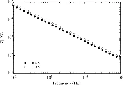
3.3.1. Impedance Measurements
The impedance measurements were performed on a Schlumberger Instruments
Model 1260 impedance/gain-phase analyzer equipped with a Solartron 1286
Electrochemical Interface. A 10 mV ac signal with a frequency sweep from 100 Hz to
100 kHz was superimposed upon a reverse dc bias stepped in 50 mV intervals between
0.4 and 1.0 V vs. Nernstian solution potential, E(A/A–
). The impedance analyzer
signal. The real and imaginary components of the impedance, Zre and Zim, respectively,
can then be calculated using the relationships Zre = Z cosq and Zim= Z sinq.
The impedance data were fit to an equivalent circuit consisting of a resistor, Rs,
representing the resistive loss across cell solution and lead, in series with a parallel circuit
containing a differential capacitance of the semiconductor space-charge region, Csc, and a
space-charge resistance, Rsc, representing resistance to Faradaic charge transfer (Figure
2.2). This model assumes that the measured differential capacitance, Cdiff, equals Csc.
The differential capacitance was computed from the impedance data using the equation:51
2 1 1 4
2
2 2
pfC Z R
Z
diff
im sc
im
= + - / (2.4)
where f is the frequency of the ac signal and Zim is the imaginary part of the measured
impedance at the dc bias of interest. The Rsc value at each dc bias was extracted from the
circular fit of the Nyquist plot. A Nyquist plot is a plot of Zim vs. Zre that shows the
branching between these two components of the measured impedance as a function of f.
At a high frequency, the effective impedance of the capacitor is small relative to Rsc and
the Csc’s contribution to Zim falls to zero. As most of the current flows through the Csc
pathway, the observed impedance is simply Rs. At a low frequency, the effective
impedance of the capacitor is high relative to Rsc, therefore most of the current flows
through the Rsc pathway, and the observed impedance is Rsc + Rs. In the
intermediate-frequency range, the changes in intermediate-frequency translate directly into the changes in the
effective impedance of the capacitor, therefore the magnitude of Z is dictated by Csc. The
differential capacitance measurements were performed in this capacitive frequency
regime where the Faradaic charge transfer pathway is suppressed.
The differential space-charge capacitance was then related to the built-in voltage
C
qN A E V
kT q
sc
d s
bi
- = Ê +
-ËÁ ˆ¯˜
2
0 2
2
ee (2.5)
where e is the dielectric constant of the semiconductor, e0 is the permittivity of free space,
Nd is the semiconductor dopant density, As is the electrode surface area, E is the applied
dc potential. By plotting Cdiff –2
vs. E (i.e., a Mott-Schottky plot) for each frequency and
extrapolating the linear regression of these data points to infinite capacitance, the Vbi of
the solid/liquid junction was calculated. To assess the validity of the equivalent circuit
model used in this experiment, the measured semiconductor dopant density was
computed from the slope of the linear fit of Cdiff –2
vs. E and compared to the value
specified by the manufacturer. Only electrodes which exhibited linear Mott-Schottky
plots (R2 .≥ 0.999, where R is the correlation coefficient) and had measured dopant
densities within the range specified by the manufacturer were included in the analysis.
Electrodes that yielded nonlinear or frequency-dependent plots were considered
defective.
3.3.2. Steady-State Current Density vs. Potential Characteristics
Current density vs. potential (J–E) measurements were performed using a
Solartron Model 1287 potentiostat or an EG&G Princeton Applied Research (PAR)
Model 173 potentiostat/galvanostat equipped with an EG&G PAR Model 175 universal
programmer. When EG&G PAR Model 173 potentiostat/galvanostat was used, traces
were recorded on a Houston Instruments Omnigraphic 2000 recorder at a scan rate of 50
mV s–1
. Light intensities were controlled by the use of a 300 W ENH-type
tungsten-halogen bulb in conjunction with neutral density filters (Hoya Optics). Open-circuit
voltages (Voc) were obtained with the sample held at open-circuit, and photocurrents (Iph)
were obtained with the samples held at 0.4 V vs. the cell potential E(A/A–
).
Photoresponse measurements were performed for both both n-GaAs/CH3CN-CoCp2
+/0
and n-GaAs/CH3CN-Fc +/0
light intensities by reading the appropriate quantities through a Fluke 27 digital
multimeter. The diode quality factors (g) and the reverse saturation current density (J0)
were extracted using the equation:52
V kT q J J oc ph = Ê ËÁ ˆ ¯˜ g ln 0 (2.6)
where k is Boltzmann’s constant, T is the temperature, and q is the charge on the electron.
The J–E characteristics of both n-GaAs/CH3CN-CoCp2 +/0
and n-GaAs/CH3
CN-Fc+/0
systems were collected mainly to confirm the reproducibility of results from prior
studies in the Lewis group. Before and after each impedance measurement, the J–E data
were obtained to verify that the properties of the electrode remained unchanged over the
time scale of the impedance study. To investigate the possibility of surface change
during the electrochemical experiments of n-GaAs in CH3CN-CoCp2 +/0
solution, the J–E
data of an n-GaAs/CH3CN-Fc +/0
contact before and after potential scans in CH3
CN-CoCp2 +/0
solution were also collected. This experiment was performed in an attempt to
observe any effect on the J–E properties of n-GaAs after electrochemical measurements
in contact with CH3CN-CoCp2 +/0
solution. An etched n-GaAs electrode was first
immersed in CH3CN-Fc
+/0
solution and a series of J–E curves were recorded in the dark
and at five different light intensities. The electrode was rinsed with CH3CN before
exposing to CH3CN-CoCp2
+/0
solution where three types of potential