2 2 0
3
CNT
D
a n
m
nm
Low Power Asynchronous UP Counter using CNTFET
V. Saravanan
V. Kannan
Research Scholar, Principal
Sathyabama University, Jeppiaar Institute of Technology
Tamilnadu, India Tamilnadu, India.
ABSTRACT
Inmany applications counter is used to divide input clock to produce output, the frequency of the output is the divide by N times of the input clock frequency. Due to these reasons ripple counters can be used as frequency dividers to reduce a high clock frequency down to a more usable value for use in digital clocks and timing applications. In many applications such as ultra low power digital circuits, nano devices, wireless communication etc, designing of low power asynchronous counter is highly desirable. This paper presents the low power asynchronous counter using carbon nanotube field effect transistor, As far as it is known, this is the first attempt to design asynchronous counter using CNTFET. Results of the design are compared with CMOS technology based asynchronous counter.
Keywords:
Ripple counter, ultra low power, nano devices, CNTFET, CMOS.
1. INTRODUCTION:
Counter circuits are used in digital systems for many purposes. They may count the number of occurrences of certain events, generate timing intervals for control of various tasks in a system, keep track of time elapsed between specific events, Frequency synthesizers, frequency dividers and so on. Counters of all kinds are used in a variety of digital circuits. The type of counters used includes binary counters, Gray code counters, ring counters, and up-down counters. Most of these counters cycle through a number of states, each state representing a natural number. Because of this cyclic behavior, the next state can be determined from the present state. An up-down counter behaves differently. It counts up or down, depending on the input received. For many counters, the value of the counter, or its count, can be read by the environment. Some- times, however, there is no need to be able to read the value of the counter.
When these counters are designed for very high speed and low power digital circuits in the nano metre ranges, CMOS technology has started to face the many difficult challenges. In CMOS technology the size of the MOSFET is scale down to reduce the size of the device. When the MOSFET scale down to the nanometer ranges, scaling has resulted in increased short-channel effects, reduced gate control, exponentially rising leakage currents, The scaling of MOSFET has progressed rapidly, it may come to an end soon because of the increased short channel effects and power-dissipation constraints. In order to overcome these problems research groups started to explore new devices to replace the CMOS technology. Many new devices has been reported such as single-electron tunneling (SET), rapid single-flux quantum logic, quantum cellular automata (QCA) and carbon nanotube field effect transistor(CNTFET)[1]-[5]. The rest of this paper is organized as follows: Section 2 describes the carbon nanotube field effect transistors. Session 3 describes the HSPICE model of CNTFET. Session 4 narrates the design of 3 bit and 4 bit as3 bit and 4 bit asynchronous up counter using
CNTFET based T-Flip Flop. Session 5 provide the simulation results and discussion. Session 6 provides conclusion.
2. CNTFET THEORY
Carbon nanotube field effect transistor (CNTFET) are currently considered, one of the main building block for the replacement of MOSFET based CMOS technology. The core of a CNTFET is carbon nanotube. CNTs are the hollow cylinders. Fig(1) shows the structure of graphene sheet and single walled carbon nanotube (SWCNT). Carbon nanotubes are formed, when a graphene sheet of a certain size that is wrapped in a certain direction, It may be either single walled or multi-walled . Two atoms in the graphene sheet are chosen, one of which servers the role as origin. The sheet is rolled until the two atoms coincide. The vector pointing from the first atom towards the other is called the chiral vector and its length is equal to the circumference of the nanotube. Depending on their chiral vector, carbon nanotubes with a small diameter are either semi-conducting or metallic in nature[6]-[8].
Carbon nanotube field effect transistors (CNTFETs) utilize semi conducting single-wall CNTs to assemble electronic devices. A single-wall carbon nanotube (or SWCNT) consists of one cylinder only, and the simple manufacturing process of this device makes
Fig (1) structure of graphene and SWCNT
it very promising alternative to today’s MOSFET. An SWCNT can act as either a conductor or a semiconductor, depending on the angle of the atom arrangement along the tube. This is referred to as the chirality vector and is represented by the integer pair (n, m). The diameter of the CNT can be calculated based on the following equation[9]-[12].
(1)
where a0 = 0.142 is the inter-atomic distance between each
3
2
3
g CNTE
aV
Vth
e
eD
2 1
1
2
/
g tot c
sg ox
G B
L
C
C
C
C
e
V
[
1
g ox Qs c
gs
tot Qs Qd
L C
C
C
C
C
C
C
, , / 2 2 /4
1
m l B
m l B km kl
E kT M L Qs E kT g
e
e
C
L
kT
e
, , , , / 2 2 /4
1
m l B ch DS
m l B ch DS
km kl
E eV kT M L
Qd
E eV kT g
e
e
C
L
kT
e
threshold voltage isdefined as the voltage required to turn ontransistor. The threshold voltage of the intrinsic CNT channel can be approximated to the first order, as the half band gap is an inverse function of the diameter and the equation for threshold voltage is given below
(2)
where a = 2.49 Å is the carbon to carbon atom distance, V
π =
3.033 eV is the carbon π-π bond energy in the tight bonding model, e is the unit electron charge, and D
CNT is the CNT
diameter. As D
CNT of a (19, 0) CNT is 1.487 nm, the threshold
voltage of a CNTFET using (19, 0) CNTs as channels, is 0.293V, The device channel consists of a (19,0), zigzag CNT with a band gap of 0.53 eV and a diameter of 1.5 nm. Fig. 2 shows the cross section of a conventional Carbon nanotube field effect transistor (C-CNTFET). The gate dielectric is a 4 nm thick HfO2 (k = 16) and the device has channel length of
18nm[14]-[16].
Fig (2) Schematic diagram of a carbon nanotube transistor
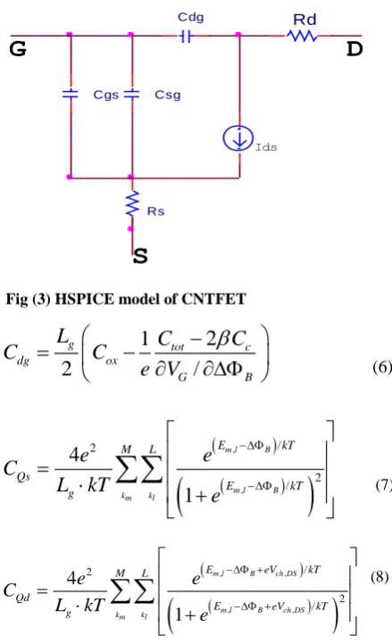
3. HSPICE MODEL OF CNTFET:
Fig (2) shows the schematic of MOSFET like CNTFET used for designing the digital circuits. It’s HSPICE model is shown in fig (3), model consists of two main parts, current sources and capacitance networks. For semi conducting sub-bands electron current is only considered for the nFET, because the hole current is suppressed by the n-type heavily doped source, drain, and usually is negligible compared to the electron current. The current contributed by the semi conducting sub-bands is given byequation (4)
(3)
J m,l ( ) is the current contributed by the substate (m,l). various capacitaces used in model are calculated by equation, (5), (6), (7),(8),(9).[17]-[20].
(4)
(5) Ids Cgs
D
S
Rd RsG
Csg CdgFig (3) HSPICE model of CNTFET
(6)
(7) (8)
Fig (4) shows the drain characteristics of carbon nanotube field effect transistor with the channel length of 18 nm. Drain voltage is varied from 0 to 0.9v for each constant value of Vgs. Current conduction of CNTFET is high due high gate capacitance. In CNTFET higk – k material is used as gate dielectric material ( k = 16 for proposed design ) which provides the high gate capacitance
Fig (4) Drain characteristics of CNTFET
4. DESIGN OF ASYNCHRONOUS UP
COUNTERS:
A counter can be constructed by a synchronous circuit or by an asynchronous circuit using flip flop. In
2
1
2
/
g tot c
dg ox
G B
L
C
C
C
C
e V
, , ,2
0,
,
km kl
M L
D m l B m l ch DS B
[image:2.595.315.535.82.443.2] [image:2.595.59.250.295.391.2] [image:2.595.314.561.530.697.2]change states at exactly the same time because they do not have a common clock pulse. The main characteristic of an asynchronous counter is each flip-flop derives its own clock from other flip-flops and hence it is independent of the input clock. therefore, the output of each flip-flop may change at different time, hence these counters are called asynchronous. From the asynchronous counter circuit diagram fig (5) It is observed that for the 3 bit counter 3 TFF is used. toggle input of the T FF is always held at logic 1 level. The outputof the first flip-flop becomes the clock input for the
Q2
HIGH
Q0
1
TFF1
CLK
T Q
Q
TFF2
1
TFF3
CLK
T Q
Q
11
CLOCK
Q1
CLK
T Q
Q
Fig (5) Design of 3 BIT asynchronous up counter using CNTFET
second flip-flop and the output of the second flip-flop becomes the clock input for the third flip-flop. For the first flip-flop, the output changes whenever there is a positive transition in the clock input. This means that the output of the first flip flop produces a series of square waves that is half the frequency of the clock input. Since the output of the first flip-flop becomes the clock of the second flip-flip-flop, the output of the second flip-flop is half the frequency of its clock, i.e. the output of the first flip-flop that in turn is half the frequency of the clock input.
In the proposed design T flip flop is used. For 3 bit asynchronous counter 3 toggle flip flop (T-FF) is employed and for 4 bit counter 4 T-FF is used. With an asynchronous circuit, all the bits in the count do not change at the same time.
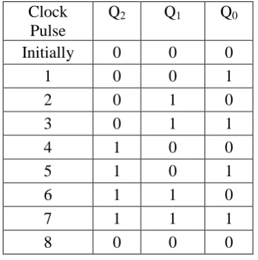
A UP counter will count up depending on the input control. Because of limited word length, the count sequence is limited. For an n-bit counter, the range of the count is 0 to 2 n-1. The count sequence usually repeats itself. When counting up, the count sequence goes in this manner: 0, 1, 2, … 2 n-2
, 2 n-1, 0, 1, …etc. The counting sequence of 3 bit counter is 0, 1, 2, ….. 7, 0, 1, …. etc. which is shown in table 1.The natural count sequence is to run through all possible combinations of the bit patterns before repeating itself. External logic can be used to arbitrary cause the counter to start at any count and terminate at any count.
[image:3.595.338.526.116.305.2]
Fig (7) shows the 4-bit asynchronous binary counter. It works exactly the same way as a 3 bit asynchronous binary counter. Except it has 16 states due to the fourth flip-flop. Asynchronous counters are commonly referred to as ripple counters dur to effect of the input clock pulse is first “felt” by T-FF1. This effect cannot get to T-FF2 immediately because of the propagation delay through T-FF1. Then there is the propagation delay through FF2 before FF3 can be triggered and so on. Thus, the effect of an input clock pulse “ripples” through the counter, taking some time, due to propagation delays, to reach the last flip-flop
Table.1. 3 bit asynchronous up counter binary state Sequence
Fig (6) simulation results of 3 BIT asynchronous up counter using CNTFET
CLK
T Q
Q
CLK
T Q
Q
Q0
CLOCK
CLK
T Q
Q
Q3
HIGH
TFF4
1
Q1
TFF3
TFF1
1
TFF2
11
CLK
T Q
Q
Q2
Fig (7) Design of 4 BIT asynchronous up counter using CNTFET
Clock
Pulse
Q
2Q
1Q
0Initially
0
0
0
1
0
0
1
2
0
1
0
3
0
1
1
4
1
0
0
5
1
0
1
6
1
1
0
7
1
1
1
[image:3.595.55.266.189.327.2] [image:3.595.315.540.343.543.2] [image:3.595.315.529.584.685.2]Table.2. 4 bit asynchronous up counter binary state sequence
Fig (8) simulation results of 4 BIT asynchronous up counter using CNTFET
5. SIMULATION RESULTS AND
DISCUSSION:
In the proposed design of 3 bit and 4 bit asynchronous counter CNTFET is used. Fig 6 shows the Simulation results of the 3 bit counter. the propagation delay tPLH of 3 bit CNTFET based counter is 40.1ps where as for
CMOS based design 8.13ns. similarly propagation delay of
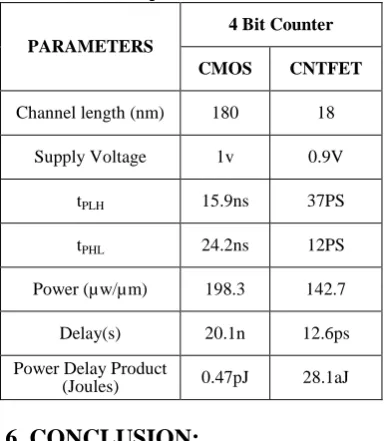
design56ps. This less propagation delay of CNTFET based design gives total delay of the 3 bit counter is 14.9ps where as in CMOS 4.1ns. Power consumption of the 3 bit CNTFET counter is 130.5 µW and for CMOS counter is 194.1µW. simulated parameters of 3 bit counter is shown in table 3. The CNTFET based 4 bit counter consumes 142.7 µW where as CMOS based design consumes 198.3 µW. delay of the counter is 12.6ps and power delay product is 28.1aJ. Simulated parameter of 4 bit counter is shown in table 4 and waveform in fig (8). from Simulated results of CNTFET based counter provides high speed of counting with low power consumption and low operating voltage. The proposed counters can be used for modern frequency synthsizer, phased locked loop, etc., Drain characteristics of the CNTFET is also simulated using HSPICE with the channel length of 18nm and with the high k dielectric material Hfo2 (k = 16). Table.3.Simulated parameters of 3 bit counter
Table.4.Simulated parameters of 4 bit counter
6. CONCLUSION:
This paper describes the design of 3 bit and 4 bit asynchronous up counter using carbon nanotube field effect transistor. Simulation is done for both CMOS and CNTFET based technology. CMOS based design is simulated in 180nm technological node and CNTFET based design is simulated in
Clock
Pulse
Q
3Q
2Q
1Q
0Initially 0
0
0
0
1
0
0
0
1
2
0
0
1
0
3
0
0
1
1
4
0
1
0
0
5
0
1
0
1
6
0
1
1
0
7
0
1
1
1
8
1
0
0
0
9
1
0
0
1
10
1
0
1
0
11
1
0
1
1
12
1
1
0
0
13
1
1
0
1
14
1
1
1
0
15
1
1
1
1
16
0
0
0
0
PARAMETERS
3 Bit Counter
CMOS CNTFET
Channel length (nm) 180 18 Supply Voltage 1v 0.9v
tPLH 8.13ns 40.1ps
tPHL 56ps 10.2ps
Power (µw/µm) 194.4 130.5 Delay(s) 4.1ns 14.9ps Power Delay Product
(Joules) 9.24-14 30.2aJ
PARAMETERS
4 Bit Counter
CMOS CNTFET
Channel length (nm) 180 18
Supply Voltage 1v 0.9V
tPLH 15.9ns 37PS
tPHL 24.2ns 12PS
Power (µw/µm) 198.3 142.7 Delay(s) 20.1n 12.6ps Power Delay Product
[image:4.595.312.505.252.457.2] [image:4.595.313.506.476.697.2]this paper to achieve high-speed operation with low power .As the threshold voltage of the CNTFET can be easily controlled by changing the chirality vector of the CNTs, digital circuit can be designed for the required threshold voltage. Since CNTFET gives the high on state current CMOS will be replaced by CNTFET for future nano devices
7. REFERENCES
[1]. Appenzeller J (2008), “Carbon Nanotubes for High-Performance Electronics Progress and Prospect”, Proceedings of the IEEE, Vol. 96, No. 2, pp. 201-211. [2]. Postma H, Teepen T, Yao Z et al. (2001), “Carbon
Nanotube Single-Electron Transistors at Room Temperature”, Science, Vol. 293, No. 5527, pp. 76-79. [3]. Radosavljevic M et al. (2003), “Drain Voltage Scaling in
Carbon Nanotube Transistors” Appl. Phys. Lett., Vol. 83, No. 12, p. 2435-2437.
[4]. Pecchia A et al. (2003), “Electronic Transport Properties of Molecular Devices”, Physical Review Letters,
Vol. 19,pp. 139-144.
[5]. Kyung Ki Kim,Yong-Bin Kim, Ken Choi (2011),“Hybrid CMOS and CNFET Power Gating in Ultralow VoltageDesign” IEEE Transactions on Nanotechnology, Vol. 10,
No. 6, Pp 1439-1448
[6]. Li J, Zhang Q, Yan Y et al. (2007), “Fabrication of Carbon Nanotube Field-Effect Transistors by Fluidic Alignment Technique”, IEEE Transactions on Nano- Technology, Vol. 6, No. 4, pp. 481-484.
[7]. Bachtold A, Hadley P, Nakanishi T and Dekker (2001), “Logic Circuits with Carbon Nanotube Transistors”, Science, Vol. 294, No. 9, pp. 1317-1320
[8]. Chen Z, Appenzeller J, Lin Y-M et al. (2006), “An Integrated Logic Circuit Assembled on a Single Carbon Nanotube”, Science, Vol. 311, No. 5768, p. 1735.
[9]. Rahman A, Jing Guo, Datta S and Lundstrom M S (2003), “Theory of Ballistic Nanotransistors”, IEEE Transactions on Electron Devices, Vol. 50, No. 10, pp. 1853-1864’ [10]. Raychowdhury A and Roy K (2005), “Carbon Nanotube
Based Voltage-Mode Multiple-Valued Logic Design”, IEEE Trans. Nanotechnology, Vol. 4, No. 2, pp. 168-179.
[11]. Han J and Jonker P (2002), “A System Architecture Solution for Unreliable Nanoelectronic Devices”, IEEE Trans. Nanotechnology,Vol.1, pp. 201-208.
[12]. Heinze S et al. (2002), “Carbon Nanotubes as Schottky Barrier Transistors”, Physical Review Letters, Vol. 89.
[13] .Ian O’Connor, Junchen Liu, etal (2007)“CNTFET Modeling and Reconfigurable Logic-Circuit Design” IEEE Transactions on Circuits and Systems, Vol. 54, No. 11, pp 2365-2379
[14] Khairul Alam, Roger Lake,l (2007) “Role of Doping in Carbon Nanotube Transistors With Source/Drain Underlaps”IEEE Transactions on Nanotechnology,Vol.6, [15]. Youngki Yoon, James Fodor, and Jing Guo,(2008) “A Computational Study of Vertical Partial-Gate Carbon-Nanotube FETs ” IEEE Transactions on Electron Devices,Vol.55,No
[16] J. Liu, I. O’Connor, D. Navarro, F. Gaffiot (2007) “Design of a Novel CNTFET-based Reconfigurable Logic Gate” IEEE Computer Society Annual Symposium on VLSI (ISVLSI'07)
[17] Jie Deng, H.-S. Philip Wong (2007) “A Compact SPICE Model for Carbon-Nanotube Field-Effect Transistors Including Nonidealities and Its Application Model of the Intrinsic Channel Region” IEEE Transactions on Electron Devices,Vol. 54, No. 12, Pp 3186-3194 [18]. Deji Akinwande, Yoshio Nishi,and H.-S. Philip Wong,
(2008) “An Analytical Derivation of the Density of States, Effective Mass, and Carrier Density for Achiral Carbon Nanotubes” IEEE Transactions On Electron Devices, Vol. 55, No. 1, Pp 289 – 297
[19] Jie Deng, H.-S. Philip Wong,(2007) “A Compact SPICE Model for Carbon- Nanotube Field-Effect Transistors Including Nonidealities and Its Application ”IEEE Transactions On Electron Devices, Vol. 54, No. 12, Pp 3195 – 3205
[20] Arijit Raychowdhury, Saibal Mukhopadhyay, and Kaushik Roy (2004) “Circuit-Compatible Model of Ballistic Carbon Nanotube Field- Effect Transistors” IEEE Transactions on Computer-Aided Design of Integrated Circuits and Systems, Vol. 23, No. 10, pp 1411 – 1420
AUTHORS PROFILE
V. Saravanan was born in vellore, Tamil nadu, India in 1981. He received his bachelor degree in Electronics and communication Engineering from Ganadhipathy Tulsi’s Engineering college, vellore, TamilNadu in the year 2004 ,ME in Applied Electronics from Sathyabama University, Chennai in the year 2007. He is presently a research scholar in the Department of Electronics and communication Engineering, Sathyabama University. He has 8 years of teaching experience. He is a life member of ISTE