Rings
PhD Thesis
written by
Orsolya K´
alm´
an
Supervisors:
Dr. Mih´aly Benedict
Dr. P´eter F¨oldi
Doctoral School of Physics
Department of Theoretical Physics
Faculty of Science and Informatics
University of Szeged
Szeged, Hungary
Contents
Part I
Introduction 1
1 Transport in mesoscopic systems 5
1.1 Semiconductor heterostructures . . . 5
1.2 Effective mass equation, transverse modes . . . 7
1.3 Experimental characterization . . . 11
1.3.1 Hall measurement . . . 12
1.3.2 High-field magnetoresistance . . . 14
1.4 Transport characteristics . . . 15
1.5 The Landauer formula . . . 17
1.6 Spin-orbit interaction . . . 21
2 Models of quantum rings 23 2.1 Interference effects in quantum rings . . . 23
2.1.1 Quantum rings . . . 24
2.1.2 The effect of magnetic field . . . 24
2.1.3 Spin-dependent interference . . . 25
2.2 Model of a quantum ring with elastic scatterers . . . 26
2.2.1 Closed ring with Aharonov-Bohm flux . . . 28
2.2.2 The scattering matrix method to couple leads to the ring . . . 29
2.2.3 Transmission probability through the ring . . . 31
2.3 Spin-dependent propagation in quantum rings . . . 32
2.3.1 The one-dimensional Hamiltonian of the ring . . . 33
2.3.2 Two-terminal ring with Aharonov-Bohm flux . . . 34
2.3.3 Two-terminal ring with Rashba spin-orbit interaction . . . 37
2.4 Conclusions . . . 40
***
Part II
3 Asymmetric injection 43 3.1 Introduction of arm-dependent asymmetry into the scattering matrix . . . 433.2 Solution of the scattering problem with arm-dependent asymmetry . . . . 46
3.2.1 No scatterers in the arms . . . 47
3.2.2 Scatterer in the arm . . . 50
4 Three-terminal quantum ring with spin-dependent propagation 55
4.1 Formal solution of the problem . . . 56
4.2 The three-terminal quantum ring as an electron spin beam splitter . . . 61
4.2.1 One input, two outputs . . . 61
4.2.2 The condition for spin polarization . . . 63
4.2.3 Polarization in a symmetric ring . . . 64
4.2.4 Polarization with asymmetric configurations . . . 67
4.2.5 Conclusions . . . 68
4.3 The physical background of spin polarization:spatial interference . . . 68
4.3.1 Spin probability currents in the ring . . . 68
4.3.2 Visualization of the effect . . . 70
4.3.3 Conclusions . . . 72
4.4 Spatial-spin correlations: intertwining . . . 72
4.4.1 Mathematical formulation of the problem . . . 73
4.4.2 The nature of spatial-spin correlations . . . 74
4.4.3 Conclusions . . . 76
5 Two-dimensional quantum ring arrays 77 5.1 Building blocks . . . 77
5.2 Properties of the conductance . . . 80
5.3 Spin transformational properties . . . 84
5.4 The effect of point-like scatterers . . . 86
5.5 Conclusions . . . 88 Summary 88 ¨ Osszefoglal´as 92 List of publications 102 Acknowlegdement 104 Appendix 106 Bibliography 108
In most of the commonly used conductors the electric current is carried by electrons. Al-though electrons have a discrete charge, diffraction experiments also have demonstrated that they propagate as waves. The wave properties of individual electrons are hardly im-portant in usual conductors the width of which is about ten million times the wavelength corresponding to an electron. The conductance of such a conductor is inversely propor-tional to its length and scales linearly with its cross-secpropor-tional area. The proporpropor-tionality coefficient, or conductivity, characterizes the material the conductor is made of, and is independent of its dimensions. One may ask: What happens with this simple scaling law when one makes a conductor thinner and shorter so that the wave property of electrons becomes relevant? This question has been in the center of interest of scientists for a long time. Due to the development in miniaturization, it became possible to fabricate conductors whose dimensions are small enough not to follow the mentioned scaling law, but still much larger than microscopic objects like atoms. These are called mesoscopic
conductors (”meso” stands for the mentioned intermediate length scale) [1,2]. The scaling law breaks down when the conductor size is small enough to allow coherent propagation of an electron across it in the given material. This happens when the dimensions of the conductor are comparable to the relevant wavelength, the mean free path and the phase relaxation length of the electrons. (These latter two notions describe the distance that an electron travels before its initial momentum or the phase of its wave function is de-stroyed, respectively.) The conductance of such small conductors is quantized in universal, material-independent units [3], and they operate as electron waveguides.
Although some of the pioneering experiments with mesoscopic conductors were per-formed using metallic conductors [4], recent works are mostly based on semiconductor heterostructures, such as AlGaAs/GaAs, or InGaAs/InAlAs. In these systems a highly mobile two-dimensional electron gas is present at the interface of the two semiconductor layers, which provides a good basis for the fabrication of mesoscopic conductors of various structure. Among these, ring shaped devices (often called quantum rings) are intensely studied due to their ability to show various types of quantum interference phenomena, such as the well-known Aharonov-Bohm effect [5], when the wave function of a charged particle passing around a magnetic flux experiences a phase shift as a result of the enclosed magnetic field.
Electrons – besides their wave nature – possess another quantum property, called spin. The idea of investigating, and possibly utilizing this additional feature in electronic trans-port led to the development of a new field of research: spintronics [6–9]. Devices, based on early results of spintronics are already commercially available, e.g., giant magnetoresis-tance (GMR) [10,11] led to computer hard drives that can store data with unprecedented surface density. An important common feature of these spintronic devices is that they use spin degree of freedom as a classical resource, quantum mechanical features play no role. In other words, spin states are ”up” and ”down” with respect to a certain quantization direction but their superpositions (preferably) play no role. The idea of utilizing spin as a quantum resource is a more recent direction in this field and may be related to the birth of quantum computing [12–15], which has attracted a lot of attention because of its potential to offer an exponential speedup over classical computation for certain prob-lems [16, 17]. A quantum computational algorithm uses quantum bits (qubits), which are two-level quantum systems represented by a two-dimensional Hilbert space, i.e., their state is an arbitrary superposition of the logical ”up” and ”down” states. Among a variety of other possibilities, electron spin has been proposed as the qubit in a quantum computa-tional system. From a practical point of view, using spin instead of charge in information processing applications may lead to less energy consumption, as spin flips require less energy than usual charge based operations. However, in order to achieve the ambitious goal of spin based computing, several problems have to be solved. Quantum information processing protocols [18] require coherent behavior, superpositions of the quantum bits must be available. From the transport point view, when the quantum mechanical infor-mation is being delivered by (spin) currents, the question whether these ”flying qubits” are practically useful is related to the nature of the transport. In the diffusive regime, when the size of the device exceeds the (spin) coherence length, no coherent behavior can be expected. Coherent manipulation of spins is possible only if the coherence length is larger than the size of the device. Currently, high mobility samples have become available such that at cryogenic temperatures spin coherence lengths [19–21] of 100 µm have been found, which mean a promising perspective in the fabrication of devices of a few microns that are capable of coherent manipulation of spins.
Semiconductor heterostructures, which have an internal electric field perpendicular to the interface between the two layers, have found great interest in spintronic research. This is due to the fact that in such systems, the manipulation of the electron spin is possible via an effect of relativistic origin. This is called Rashba spin-orbit interaction [22]: in the particle’s rest frame there is a magnetic field perpendicular to the electric field and the direction of movement. The spin direction precesses around the axis parallel to this magnetic field and the precession rate depends on the spin-orbit interaction strength, which can be controlled by an external gate voltage [23, 24].
in-teraction [25–28] is the spin field-effect transistor proposed by Datta and Das [25]. In this proposal, a spin-polarized electron is injected from a ferromagnetic source contact into a two-dimensional electron gas. The electron then undergoes spin precession due to the Rashba effect before it is collected by a ferromagnetic drain contact. By varying the strength of the spin-orbit coupling with an applied gate voltage, one can alter the degree of spin precession and thus modulate the current through the device. Another device that has received considerable attention is the spin-interference device proposed in Ref. [29]. This is a small ring (with a diameter of a micron) connected with two external leads fabri-cated in a semiconductor heterostructure with Rashba spin-orbit interaction. The key idea is that the phase difference between electrons traveling clockwise and counterclockwise would produce interference effects in the spin-sensitive electron transport. The conduc-tance oscillations of such a ring, fabricated in InGaAs/InAlAs and in HgTe/HgCdTe, has been experimentally demonstrated in Refs. [30] and [31], respectively. Rectangular arrays of such rings have also been realized and measured experimentally [32,33]. Of the theoret-ical results concerning quantum rings with Rashba spin-orbit interaction here we mention Ref. [34] where it has been shown that the interference effects lead to the modification of the spin properties of the incoming electron by the spin-orbit interaction, resulting in a transformation of the qubit state carried by the spin [34], which can be varied by tuning the strength of the Rashba interaction, by changing the relative position of the leads, or the size of the ring.
The ongoing intensive experimental [31–33] and theoretical [35–37] interest in quantum rings with Rashba spin-orbit interaction and/or magnetic field motivated us to carry out further investigations regarding such rings. We wished to describe a quantum ring connected to two current-carrying leads, in which the probabilities for the electron to enter the two arms of the ring are not equal. We also wished to explore whether it is possible to polarize the spin of the electron by a quantum ring in which Rashba coupling is present. Additionally, we intended to calculate the conductance of rectangular arrays with Rashba spin-orbit interaction and a perpendicular magnetic field.
This dissertation is organized as follows. In Part I we summarize the results known form the literature: in Chapter 1 we give an introduction to the basic properties of transport in mesoscopic systems. Then, in Chapter 2 we overview interference effects that may be present in quantum rings and introduce one-dimensional models that are used in their theoretical description, which are based on the fact that when the width of the rings is much smaller than their radii, then, at low enough temperatures only the lowest radial mode takes part in the conduction. One of the models (Sec. 2.2) is able to take into account the imperfectness of the coupling between the current-carrying leads and the ring. It is also inherently able to account for scatterers in the arms of the ring. The other model (Sec. 2.3) considers no additional reflections at the junctions of the leads with the ring (when no scatterers are placed there directly), it simply fits the wave
functions and the currents at a given junction, and considers no scatterers in the arms of the ring. We will use this latter model to take into account spin-orbit interaction in the ring.
In Part II we present our own results: We extend the use of the above mentioned models in several aspects. In Chapter 3, we modify the model presented in Sec. 2.2 in order to be able to take into account asymmetric injection into the arms of a ring, in the presence of a magnetic field, and a scatterer in the ring. Chapter 4 is dedicated to the investigation of the effects related to a three-terminal quantum ring with Rashba spin-orbit coupling. In Section 4.1 we solve the scattering problem of such a ring with the model presented in Section 2.3. Then, in Section 4.2 we discuss our proposal for its utilisation, namely, spin-polarization: we show that the incoming electrons are forced to split into two different spatial parts and due to spin-sensitive quantum interference, electrons that are initially in a totally unpolarized spin state become polarized at the outputs with different spin directions. In Section 4.3 we analyze the physical origin of this spin polarizational effect, and demonstrate that it is due to spatial interference. In Section 4.4 we investigate the correlations between the spatial degree of freedom of the electron and its spin when leaving a three-terminal ring. We show that quantum intertwining between the spin direction and the output path can be present. In Chapter 5 we study electron transport through multi-terminal rectangular arrays of quantum rings in the presence of Rashba spin-orbit interaction and of a perpendicular magnetic field. We show that due to destructive and constructive interferences, the conductance shows oscillations as a function of the wave vector, the spin-orbit coupling strength, and the magnetic field.
Transport in mesoscopic systems
In recent years miniaturization led to a dramatic increase of interest in the physics and applications of structures which can be described as ”low-dimensional”. In the case of electronic transport, this term refers to a system in which electrons are constrained by potential barriers so that they lose one or more degrees of freedom for motion; the system becomes two, one or even zero dimensional. Although a large variety of systems has been proposed, the majority of work on two- (and lower- ) dimensional systems has been performed on semiconductor structures.
In this chapter we summarize the basic transport properties of low-dimensional sys-tems relying mainly on Ref. [1]. We note that here we do not deal with zero-dimensional systems as they were not part of our investigations. In Section 1.1 we give an overview of the systems that are most frequently used as a basis for the fabrication of low-dimensional nanostructures. In Section 1.2 we present a simple theoretical description of two- and one-dimensional conductors, and then, in Section 1.3 we show the most important experimen-tal measurements that are used for the characterization of these devices. In Section 1.4 we describe the characteristics of transport and then, in Section 1.5 we present the Landauer formula which relates the experimentally measurable conductance to the transmission probability through the conductor which can be obtained from its quantum mechanical description.
1.1
Semiconductor heterostructures
Currently, semiconductor heterostructures provide a good perspective for investigations of electrical conduction on short length scales. This was made possible by the availability of semiconducting materials of unprecedented purity and crystalline perfection. Such materials can be structured to contain a thin layer of highly mobile electrons. Motion perpendicular to the layer is quantized, and the electrons are constrained to move in a plane. This system combines a number of desirable properties, not shared by thin metal
films. It has a low electron density, which may be varied by means of an electric field. As we will see in Section 1.2 the low density implies a large wavelength corresponding to conduction electrons, that is comparable to the dimensions of the nanostructures that can be fabricated today. Additionally, compared to bulk samples, the electron mean free path can be quite large in these systems. As a result, quantum effects are manifested in the experimentally measurable quantities, such as the conductance.
y z x Surface n-AlGaAs i-GaAs spacer z E Ec EF Ev z E 2-DEG EF Ec Ev (a) (b)
Figure 1.1: Conduction and valence band line-up at a junction between an n-type AlGaAs and intrinsic GaAs, (a) before and (b) after charge transfer has taken place. Note that this is a cross-sectional view.
One of the heterostructures that were first used for two-dimensional transport is com-posed of the two semiconductors, GaAs and AlxGa1−xAs which have nearly the same
lat-tice parameter. In the latter material, a fraction x (commonly x' 0.3) of the Ga atoms in the GaAs lattice is replaced by Al atoms. For x <0.45 the semiconductor AlxGa1−xAs
has a direct band gap, larger than that of GaAs, being approximately proportional to the Al content. Let us now consider the conduction and valence band line-up perpendicular to the interface (z-direction) when we first bring the layers in contact (Fig. 1.1(a)). The Fermi energy EF in the widegap AlGaAs layer is higher than that in the narrowgap GaAs
layer. Consequently, some of the electrons introduced by the donors in the n-AlGaAs are transferred into the lower-lying conduction band of the GaAs, leaving behind positively charged donors. This space charge gives rise to an electrostatic potential that causes the bands to bend as shown in Fig. 1.1(b), forming a nearly triangular well. At equilibrium the Fermi level is constant everywhere. The electron density is sharply peaked near the GaAs-AlGaAs interface (where the Fermi level is inside the conduction band) forming
a thin conducting layer which is usually referred to as the two-dimensional electron gas (2-DEG in short). In the narrow (∼5 nm) well formed at the heterojunction, the energy spectrum for motion perpendicular to the interface is discrete (and in most cases only one electric subband is populated), whereas the motion along the interface is free-electron-like with an effective mass close to that of bulk GaAs conduction band electrons.
The carrier mobility of semiconductor heterostructures can be considerably larger than that of the corresponding bulk semiconductor; this is achieved by a technique generally referred to as ”modulation doping”. Modulation-doped heterostructures are obtained by introducing n-type dopant impurities (e.g., Si) into the wide-band-gap material, AlGaAs at some distance from the interface (the undoped AlGaAs is called the spacer), whereas the narrow-band-gap material (GaAs) remains free from intentional doping, as shown in Fig 1.1(a). Due to modulation doping, the mobile carriers in the heterostructure are spatially separated from their parent impurities [38] which leads to a reduction of scattering. Thus, high carrier mobilities can be obtained.
Although AlGaAs/GaAs has served as a model system for the majority of investiga-tions of transport in low-dimensional structures, other material combinainvestiga-tions have also received considerable attention. Important among these have been heterojunctions in InGaAs/InAlAs and HgTe/HgCdTe [39]. The InGaAs/InAlAs system has a number of potential technological advantages over AlGaAs/GaAs, such as a lower electron effective mass and a larger energy separation between conduction band minima in InGaAs/InAlAs compared with AlGaAs/GaAs, however, the presence of alloy scattering results in rela-tively low mobilities at low temperatures [40]. Work on HgTe/CdHgTe has indicated that many more subbands are occupied than what are usually observed in other heterojunction systems [41].
1.2
Effective mass equation, transverse modes
In order to determine theoretically the electronic states in solids, approximations of dif-ferent accuracy have been developed. In this dissertation we will use the approximation that electrons are independent. In the single-electron picture it is also assumed that each electron feels the same periodic potential. Then, the wave function of an electron is a Bloch wave: the product of a plane wave and a lattice periodic function. For a given wave number (it is sufficient to consider only those in the first Brillouin zone) one can determine the corresponding energies. For bulk semiconductors these energies form bands, the two uppermost being the conduction and the valence band, which are separated by a band gap. As the Fermi level is inside the band gap, the valence band is full and the conduc-tion band is empty. Conducconduc-tion may only happen when valence electrons gain energy from thermal excitation. Only those electrons take part in the conduction, which have
an energy close to the minimum of the conduction band. For these conduction electrons the Hamiltonian can be approximated by an effective free-electron-like operator that is the sum of the energy corresponding to the conduction band edge and a kinetic term that incorporates the effect of the periodic lattice potential through the effective mass. The eigenfunctions of this Hamiltonian no longer reflect the periodicity of the crystal.
When two semiconductor crystals are placed adjacent to each other to form a het-erojunction, then similar eigenvalue equations are valid in each, remembering that the effective mass could be a function of position. Thus, the dynamics of electrons in the conduction band can be described by an equation of the form
· Ec+ P2 2m∗ +U(r) ¸ Ψ(r) =EΨ(r) (1.1)
whereP is the momentum operator of the electron, U(r) is a model potential energy due to space-charge and confinement, Ec is the energy corresponding to the conduction band
edge, and m∗ is the effective mass. As we have already mentioned, the lattice potential, which is periodic on an atomic scale, does not appear explicitly in Eq. (1.1); its effect is incorporated through the effective mass m∗ which we assumed here to be spatially constant. Any band discontinuity ∆Ec at heterojunctions is incorporated by letting Ec
be position-dependent. We note that in the presence of a magnetic field P has to be replaced by P −eA, where e is the charge of the electron, which is the negative of the elementary charge, and A is the vector potential. Equation (1.1) is called a single-band effective mass equation.
In a 2-DEG shown in Fig.1.1(b), the electrons are free to propagate in thex−y plane but are confined by some potentialU(z) in thez-direction. The electronic wave functions in such a structure can be written e.g., in the form
Ψ(r) = φl(z)eikxxeikyy, (1.2)
with the dispersion relation:
E =Ec+εl+ ~2 2m∗ ¡ k2 x+ky2 ¢ . (1.3)
The index l labels the different subbands each having a different wave function φl(z) in
the z-direction and a cut-off energy εl. Usually at low temperatures with low carrier
densities only the lowest subband with l = 1 is occupied and the higher subbands do not play any significant role. We can then ignore the z-dimension altogether and simply treat the conductor as a two-dimensional system in the x−y plane. For a free electron gas the eigenfunctions are obtained from Eq. (1.1) by setting U = 0. The eigenfunctions
normalized to an areaS have the form
Ψ(x, y) = √1
Se
ikxxeikyy, (1.4)
with eigenenergies given by
E =Es+ ~2 2m∗ ¡ k2 x+k2y ¢ , (1.5) whereEs =Ec+ε1.
At equilibrium the available states in a conductor are filled up according to the Fermi function
f0(E) =
1 1 +eEk−BETF
, (1.6)
whereEF is the Fermi level, which, atT = 0 K, coincides with the Fermi energy. (We note
that in the literature, instead of Fermi level often the terminology ”chemical potential” is used, here however, the sample properties do not change significantly, therefore we will continue using ”Fermi level”.) In the low temperature limit (eEsk−BETF ¿ 1), the Fermi
function inside the band (E > Es) can be approximated by
f0(E) = Θ (EF−E). (1.7)
where Θ is the unit step function. We note that throughout this thesis we will remain within this limit.
At low temperatures the conductance is determined entirely by electrons with energy close to the Fermi level. The wavenumber of such electrons is referred to as the Fermi wavenumber (kF): kF = p 2m∗(E F−Es) ~ . (1.8)
As EF − Es is proportional to the number of occupied states in two dimensions, and
consequently to the equilibrium electron densityns, we can express the Fermi wavenumber
as:
kF =
√
2πns. (1.9)
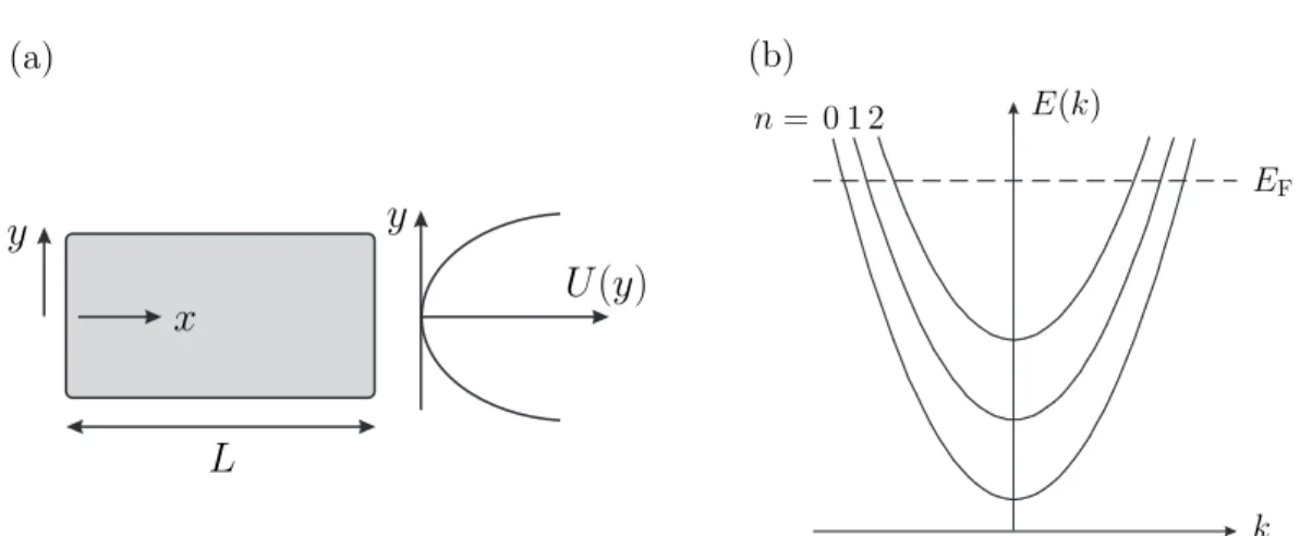
In narrow conductors, besides the z-direction, electrons are also confined in a second direction. Let us consider a rectangular conductor that is uniform in the x-direction, which has some transverse confining potentialU(y) (see Fig. 1.2(a)). Then, the solutions of the effective mass equation (1.1) can be expressed in the form of plane waves
Ψ(x, y) = √1
Le
where L is the length of the conductor over which the wavefunctions are normalized. In general, for arbitrary confining potentials χ(y) can not be determined analytically. However, for a parabolic potential U(y) = 1
2m∗ω20y2, which is often a good description
of the actual potential in narrow conductors, analytic solutions can be written down. The eigenenergies and eigenfunctions are well-known from the theory of the harmonic oscillator [42].
y
x
y
U
(
y
)
L
(a) E(k) EF k n= 0 1 2 (b)Figure 1.2: (a) A rectangular conductor assumed to be uniform in the x-direction and having some transverse confining potentialU(y). (b) Dispersion relation,E(k) as a function ofkfor electric subbands arising from parabolic confinement. The different subbands are indexed by n.
The dispersion relation is sketched in Fig. 1.2(b). States with different indexnare said to belong to different subbands just like the subbands that arise from the confinement in the z-direction. The spacing between two subbands is equal to ~ω0. The tighter
the confinement, the larger ω0 is, and the further apart the subbands are. Usually the
confinement in the z-direction is very tight (electrons are confined into a layer of width of ∼ 5−10 nm) so that the corresponding subband spacing is large (∼ 100 meV) and only one or two subbands are customarily occupied. In all our discussions we will assume that only one z-subband is occupied. The y-confinement is relatively weaker and the corresponding subband spacing is smaller so that a number of these may be occupied under normal operating conditions. The subbands are called transverse modes in analogy with the modes of an electromagnetic waveguide, and such conductors are often referred to as electron waveguides.
As a simple estimation for the number of transverse modes in a narrow quantum wire of width W, one may also consider the transverse confining potential as an infinite well, the discrete energies of which are given as n2
W~2π2/(2m∗W2) (nW = 1,2, ...). Then, the
energy difference between the first and second energy levels in the case of a narrow wire of width W = 50 nm, is approximately twice as much as the Fermi energy (for a Fermi energy of 11.13 meV in case of an effective mass m∗ = 0.023m of InGaAs), however, as
W is increased, this ratio is decreased, so that in the case of W = 100 nm, two of these modes may be occupied.
1.3
Experimental characterization
In this section we summarize some of the experimental tools which are used to determine the characteristic parameters of the two-dimensional electron gas formed at the interface of semiconductor heterostructures. We will describe magnetoresistance measurements in low and high magnetic fields, from which the mobility and the carrier concentration in the sample can be derived.
The mobility (at low temperatures) provides a direct measure of the momentum re-laxation time, which is limited by impurities and defects. Let us first briefly explain the meaning of mobility. In equilibrium the conduction electrons move in a random way, not producing any current in any direction. An applied electric field E gives them a drift velocity vd in the direction of the force eE. In order to relate the drift velocity to the
electric field we note that, at steady-state, the rate at which the electrons receive momen-tum from the external field is exactly equal to the rate at which they lose momenmomen-tum due to scattering processes: · dp dt ¸ scattering = · dp dt ¸ field . (1.11)
From this follows that
m∗v
d
τm
=eE, (1.12)
where τm is the momentum relaxation time. The drift velocity of electrons is thus given
by
vd =
eτm
m∗E. (1.13)
The mobility is defined as the ratio of the drift velocity to the electric field:
µ= ¯ ¯ ¯vd E ¯ ¯ ¯= |e|τm m∗ . (1.14)
Mobility measurement using the Hall effect (see Section 1.3.1) is a basic characterization tool for semiconductor samples, since, if the mobility is known, the momentum relaxation time can easily be deduced from Eq. (1.14).
In bulk semiconductors as we decrease the temperature, at first, the momentum re-laxation time increases due to the suppression of scattering on phonons. However, it does not increase any further when the scattering on phonons becomes weak enough so that scattering on impurities becomes the dominant mechanism. In undoped samples, the mo-bilities are higher, but these are less useful since there are very few conduction electrons. In a 2-DEG, on the other hand, mobilities may be two orders of magnitude larger than in undoped samples. This is due to modulation doping, i.e., the spatial separation between the donor atoms in the AlGaAs layer and the conduction electrons in the GaAs layer, which reduces the scattering on impurities.
1.3.1
Hall measurement
The measurement of conductivity in a weak magnetic field (generally referred to as a Hall measurement) is one of the basic tools used to characterize semiconductor samples. This is due to the fact that it allows the determination of the carrier density ns and the
mobility µ individually, while the conductivity measured without a magnetic field only gives the product of these two.
In a magnetic field at steady-state, the rate at which the electrons receive momentum from the external field is equal to the rate at which they lose momentum due to scattering processes:
m∗v
d
τm
=e(E+vd×B). (1.15)
AssumingB = ˆzB and using the fact that the current densityJ is related to the electron density ns by the relation J =evdns, we can rewrite Eq. (1.15) in the form
à Ex Ey ! = 1 σ à 1 −µB µB 1 ! à Jx Jy ! , (1.16)
where σ ≡ |e|nsµis the conductivity, and µ≡ |e|τm/m∗. Since the resistivity tensor ρ is
defined by the relation E=ρJ, we can write from Eq. (1.16)
ρxx =ρyy = 1/σ, (1.17)
ρyx =−ρxy = µB/σ =B/(|e|ns). (1.18)
Thus this simple Drude model predicts that the longitudinal resistance is constant while the Hall resistance increases linearly with the magnetic field.
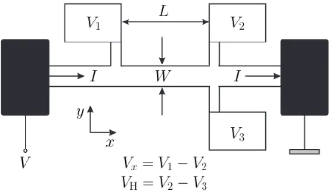
V x y I W I L V1 V2 V3 Vx=V1−V2 VH=V2−V3
Figure 1.3: Rectangular Hall bar for magnetoresistance measurements. The magnetic field is in the
z-direction, perpendicular to the plane of the conductor.
Experimentally, the resistivity tensor is measured by preparing a rectangular sample, setting up a uniform current flow along the x-direction and measuring the longitudinal voltage drop Vx = V1−V2 and the transverse (or Hall) voltage drop VH = V2 −V3, as
the width of the sample, the resistivities ρxx and ρyx are related to the longitudinal and transverse voltages by ρxx = Vx I W L, (1.19) ρyx = VH I . (1.20)
The carrier densitynsand the mobilityµcan be obtained from the measured resistivities
ρxx and ρyx using Eqs. (1.17) and (1.18):
ns = · |e|dρyx dB ¸−1 = I |e|dVH dB (1.21) µ = 1 |e|nsρxx = IL |e|nsVxW (1.22)
For this reason, Hall measurement is a basic characterization tool for semiconducting samples.
Figure 1.4: Measured longitudinal and transverse voltages for a modulation-doped GaAs sample at
T = 1.2 K (I= 25.5µA) [43].
Figure 1.4 shows the measured longitudinal voltage Vx and transverse voltage VH for
a modulation-doped GaAs sample using a rectangular Hall bar with W = 0.38 mm and
L = 1 mm and a current of I = 25.5 µA [43]. At low magnetic fields the longitudinal voltage is nearly constant while the Hall voltage increases linearly in agreement with the predictions of the semiclassical Drude model described above. At high fields, however, the longitudinal resistance shows an oscillatory behavior, referred to asShubnikov-deHaas (or SdH) oscillations, while the Hall resistance exhibits plateaus corresponding to the minima in the longitudinal resistance. These features are usually absent at room temperature but quite evident at cryogenic temperatures. These features can be understood by taking into account the formation of Landau levels.
1.3.2
High-field magnetoresistance
As we have mentioned in the previous section the comparison of the experimental data shown in Fig. 1.4 is in disagreement with the predictions of the Drude model at high magnetic fields. There are (SdH) oscillations in the longitudinal resistivity ρxx. The
minimum longitudinal resistivity ρxx is very close to zero and plateaus appear in the Hall
resistivity ρyx whenever ρxx goes through a minimum.
As it is well-known from quantum mechanics, at high magnetic fields, the energy of electrons becomes quantized, forming the so-called Landau levels [44], which have the same form as those of the quantum harmonic oscillator. In a 2-DEG, which is confined in the z-direction, they can be written as
Enl =Es+~ωc µ nl+ 1 2 ¶ , nl = 0,1,2, ... (1.23)
whereωc=|e|B/m∗ is the cyclotron frequency. Landau levels are degenerate, the number
of electrons per level (N) is directly proportional to the strength of the applied magnetic field [45]
N = 2|e|B
h . (1.24)
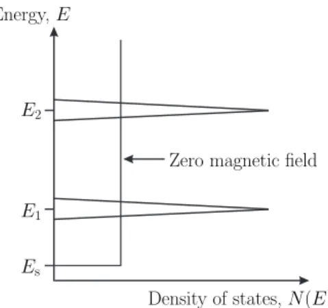
The SdH oscillations that can be seen in Fig. 1.4, arise because the step-like density of states associated with a 2-DEG breaks up into a sequence of peaks spaced by ~ωc,
due to the formation of Landau levels. This is illustrated in Fig. 1.5. The spikes are ideally delta functions, but in practice scattering processes spread them out in energy. As the magnetic field B is changed, the spacing of Landau levels increases. The resistivity
ρxx goes through one cycle of oscillation as the Fermi level moves from the center of one
Landau level to the center of the next one. This provides a simple method to calculate the electron density ns from the oscillations in ρxx.
Es E1 E2 Energy,E
Density of states,N(E) Zero magnetic field
Figure 1.5: Density of states as a function of the energy for a 2-DEG in a magnetic field.
As we change the magnetic field B the number of occupied Landau levels changes. The resistivityρxx goes through a maximum every time this number is a half-integer and
the Fermi level lies at the center of a Landau level. Therefore, the magnetic field values
B1 and B2 corresponding to two successive peaks must be related by
ns 2|e|B1/h − ns 2|e|B2/h = 1 (1.25) so that ns = 2|e| h 1 1 B1 − 1 B2 . (1.26)
We could choose many different valuesB1 and B2 corresponding to any pair of successive
peaks. They should all yield approximately the same result for the carrier density. The usual procedure is to plot the positions of the maxima in ρxx as a function of 1/B, then
the slope of the resulting straight line gives the electron density.
1.4
Transport characteristics
We have seen in Sec. 1.3 that for a given sample the electron densityns and the mobility
µ can be measured experimentally, and the momentum relaxation time τm can be
de-rived. Since impurities, lattice vibrations (phonons) or electron-electron interaction lead to ”collisions” that scatter the electron from one state to another, thereby changing its momomentum, the momentum relaxation timeτm is related to the collision time τc (the
average time between two collisions) by a relation of the form 1
τm
= 1
τc
α, (1.27)
where 0 ≤ α ≤ 1 denotes the ”effectiveness” of an individual collision in destroying momentum: if the collisions are such that the electrons are scattered only by a small angle, then very little momentum is lost in an individual collision, i.e.,α is very small so that τm is much longer than τc. The mean free path L is the distance that an electron
travels before its initial momentum is destroyed, that is,
L=vFτm, (1.28)
where vF is the Fermi velocity (the velocity of electrons at the Fermi level), which, for a
free two-dimensional electron gas, can be given in the following way:
vF = ~kF m∗ = ~ m∗ √ 2πns. (1.29)
When estimating L we used the fact that at low temperature, electrons with energies close to the Fermi level are responsible for the conduction. However,L is usually smaller than what we can calculate from Eq. (1.28), as the velocity of an electron is generally
smaller than vF. In high mobility semiconductors at low temperature, the typical value
of the mean free path is 10−100 µm. In samples, which are smaller thanL, electrons are transported essentially without disturbance, i.e., ballistically.
The mean free path is related to the momentum relaxation of the electrons. If however, we want to treat the electrons quantum mechanically, there is another characteristic length, the one that is related to phase relaxation. Let us consider the process, when the phase of the wave function of the electron is initially well-defined, but becomes more and more random as a consequence of scattering events. The characteristic time of this phenomenon is the phase relaxation time τϕ, which can be related to τc by:
1
τϕ
= 1
τc
β. (1.30)
In general, τm and τϕ are not necessarily of the same magnitude. One way to visualize
the destruction of phase is in terms of a thought experiment involving interference. For example, let us suppose that we split a beam of electrons into two paths of equal length and then recombine them. In a perfect crystal the two paths would be identical resulting in constructive interference. By applying a magnetic field perpendicular to the plane con-taining the paths, one can change their relative phase, thereby changing the interference alternately from constructive to destructive and back. Now let us suppose that we are not in a perfect crystal but in a real one with collisions due to impurities, phonons etc. We would expect the interference amplitude to be reduced by a factor e−τϕτt, where τ
t is
the transit time that the electron spends in each arm of the interferometer.
Let us investigate what happens if we introduce impurities and defects randomly into each arm. The two arms are then no longer identical so that the interference may not be constructive at zero magnetic field. But as long as the impurities and defects are static, there is a well-defined phase-relationship between the two paths, and as we increase the magnetic field we would go through alternate cycles of constructive and destructive interference, whose amplitude is unaffected by the length of each arm. We may thus conclude that for static scatterers β= 0 in Eq. (1.30).
The situation is different when we take into account the effect of dynamic scatterers, like lattice vibrations (phonons). The phase-relationship between the scattered waves in the two arms then varies randomly with time so that there is no stationary interference pattern. At a fixed value of the magnetic field the scattered waves show random variations from constructive to destructive interference which time-average to zero. Interference can only be observed between the unscattered components, whose amplitude decreases exponentially with the length of each arm.
If the internal state of a scatterer can be changed as a result of a collision with an electron, then it can ruin the interference. This is related to the fact that interference can be expected only if there is no way to tell which path the electron took. But if there is a
high probability that the electron changes the internal state of a scatterer in one arm of the interferometer, then in principle, one could tell which path it took.
Another important source of phase-randomizing collisions is electron-electron interac-tion. Electrons are scattered by other electrons due to their mutual Coulomb repulsion. Interestingly, the mean free path (L) is not affected by such processes. This is because they do not lead to any loss in the net momentum, as any momentum lost by one electron is picked up by another. Consequently, the effectiveness factorα is zero for such processes thoughβ is non-zero.
We have seen that the characteristic time of momentum and phase depend in a different way on the different type of scattering mechanisms, thus in general, they are not the same. In certain low-mobility semiconductors, often τϕ À τm, then, as a result of numerous
elastic scattering events with static scatterers, the corresponding classical motion is quasi-random, but the phase coherence is kept. In high-mobility samples however, in general
τm ≈τϕ, and the phase-relaxation length Lϕ is given by
Lϕ =vFτϕ, (1.31)
and it is essentially equal to the mean free path L. In this case the size of the sample determines whether the behavior is coherent or incoherent. If the electrons are transported in samples that are much larger than Lϕ, then no quantum effects can be expected. But
if the size of the sample is smaller than Lϕ, then quantum mechanical description is
necessary.
1.5
The Landauer formula
In this section we describe the Landauer formula [46] that has proved to be very useful in describing mesoscopic transport. In this approach, the current through a conductor is expressed in terms of the probability that an electron can be transmitted through it.
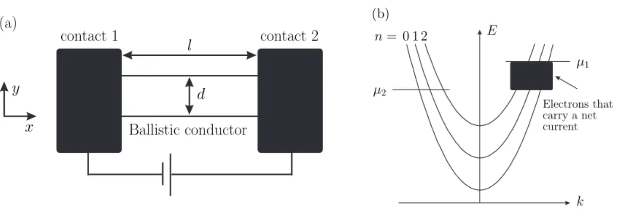
Let us consider a piece of conductor placed between two large contact pads as shown in Fig. 1.6(a). If the dimensions of the conductor were large, then its conductance would be given by G = σd/l, where the conductivity σ is a parameter characteristic of the material but independent of the dimensions of the sample. If this ohmic scaling relation were to hold as the length (l) is reduced, then we would expect the conductance to grow indefinitely. Experimentally, however, it is found that the measured conductance approaches a limiting value Gc, when the length of the conductor becomes much shorter
than the mean free path. This is rather counterintuitive since a ballistic conductor (that is, a conductor with no scattering) should have zero resistance.
The resistance G−1
c arises from the interface between the conductor and the contact
(a) y x contact 1 contact 2 l d Ballistic conductor (b) E µ1 k n= 0 1 2 µ2 Electrons that carry a net current
Figure 1.6: (a) A conductor is placed between two contacts across which an external bias is applied. (b) Dispersion relations for the different transverse modes (or subbands) in the narrow conductor.
resistance. The current is carried in the contacts by infinitely many transverse modes, but inside the conductor by only a few modes. This requires a redistribution of the current among the current-carrying modes at the interface leading to the interface resistance.
To determine the contact resistanceG−1
c we consider a ballistic conductor and calculate
the current through it for a given applied bias (µ1−µ2)/e. It is straightforward to calculate
this current if we assume that the contacts are ”reflectionless”, that is, the electrons can enter them from the conductor without suffering reflections. We use the quotes to remind that the reflection is negligible only when transmitting from the narrow conductor to the wide contact. Going the other way from the contact to the conductor, the reflections can be quite large.
For ”reflectionless” contacts, we have a simple situation: +k states in the conductor are occupied only by electrons originating in the left contact while −kstates are occupied only by electrons originating in the right contact. This is because electrons originating in the right contact populate the−kstates and empty without reflection into the left contact while electrons originating in the left contact populate the +k states and empty without reflection into the right contact (note that k denotes the wavenumber in the x-direction, shown in Fig. 1.6(a)).
We will now argue that the Fermi level for the +k states is always equal to µ1 even
when a bias is applied (Fig. 1.6(b)). Suppose both contacts are at the same potential µ1.
There is no question then that the Fermi level for the +k states (or any other state) is equal to the potential µ1. Now if we change the potential at the right contact to µ2, this
can have no effect on the Fermi level for the +k states since there is no causal relationship between the right contact and the +k states. No electron originating from the right contact ever makes its way to a +k state. Similarly, we can argue that the Fermi level for the −k states is always equal to µ2. Hence at low temperatures the current is equal
To calculate the current we note that the states in the narrow conductor belong to different transverse modes or subbands, as discussed in Section 1.2. Each mode has a dispersion relation E(n, k) as sketched in Fig. 1.2(b) with a cut-off energy
εn =E(n, k = 0), (1.32)
below which it cannot propagate. The number of transverse modes at an energy E is obtained by counting the number of modes having cut-off energies smaller than E:
M(E) =X
n
Θ(E−εn). (1.33)
We can evaluate the current carried by each transverse mode (labeled by n) separately and add them up.
Let us consider a single transverse mode whose +k states are occupied according to some function f+(E) (in the low temperature limit this function is given by f+(E) =
Θ(µ1 −E)). A uniform electron gas with ne electrons per unit length moving with a
velocity v carries a current equal to enev. Since the electron density associated with a
singlek-state in a conductor of length l isne= 1/l, and its velocity is given by v = ~1dEdk,
we can write the current I carried by the +k states as
I = e l X k vf+(E) = e l X k 1 ~ ∂E ∂kf +(E). (1.34)
Assuming periodic boundary conditions and converting the sum over k into an integral according to the usual prescription
X k →2 l 2π Z dk,
where the factor 2 takes into account the spin of the electron, we obtain
I = 2e
h Z ∞
max(εn,µ2)
f+(E)dE, (1.35)
where εn is the cut-off energy of the waveguide mode. If εn < µ2, and we are in the
low-temperature limit, then we can easily calculate the integral (1.35):
I = 2e
h (µ1−µ2). (1.36)
From this follows that the contact resistance is
G−1 c = (µ1 −µ2)/e I = h 2e2. (1.37)
For a single-moded conductor the contact resistance is ∼12.9 kΩ, which is certainly not negligible. This is the resistance one would measure if a single-moded ballistic conductor were placed between two conductive contacts.
Assuming that M modes carry the current the contact resistance (which is the resis-tance of a ballistic waveguide) is given by
G−1 c =
h
2e2M, (1.38)
i.e., it is inversely proportional to the number of modes. This means that in the macro-scopic limit, when M is very large, the contribution of the contact resistance to the full resistance is negligible. If however, M is sufficiently small, then the appearance of a new mode leads to a measurable decrease in the resistance.
It is important to note that the contact resistance arises because on one side the current is carried by infinitely many modes, while on the other side it is carried only by a few modes. The details of the geometry are not important as long as the contacts are ”reflectionless” as explained earlier.
Let us now consider the case when there is scattering inside the ballistic conductor (e.g. due its geometry or impurities). Then those electrons which have entered the conductor not necessarily exit from it. This leads to a resistance greater than G−1
c . As we explained
above, the current that enters the conductor is
Iin=
2e
h M(µ1−µ2). (1.39)
If, for simplicity, we consider the probability T that an electron transmits the conductor to be equal for each mode, then the current which flows out of the conductor is
Iout =T
2e
hM(µ1−µ2), (1.40)
from which for the conductance we get
G= 2e
2
h MT. (1.41)
This is the Landauer formula. The factor T represents the probability that an electron injected at one end of the conductor will be transmitted to the other end. If the transmis-sion probability is unity, we recover the correct exprestransmis-sion for the resistance of a ballistic conductor including the contact resistance (see Eq. (1.38)).
1.6
Spin-orbit interaction
In this section we recall a relativistic effect, namely, spin-orbit interaction, that is common in semiconductor heterostructures either due to the inversion asymmetry in the bulk crystal, or to the asymmetry in the growth direction of the heterostructure. As we will see in the next chapters, devices with such interactionmay find interesting applications.
Taking an expansion of the Dirac equation up to second order in P2/m2c2 [47, 48],
the most important correction to the nonrelativistic (Pauli) limit is the appearance of the term in the Hamiltonian called thespin-orbit interaction1:
HSO =− ~
4m2c2σ·(P ×∇V) (1.42)
as it induces a splitting of the energy levels due to spin, even in the absence of an ex-ternal magnetic field. The other second order corrections are spin independent and in a perturbative treatment yield only additive constants, and have no effect on the spectrum. Therefore we have the following effective Hamiltonian for an electron in the potential V:
H = 1
2m(P −eA)
2+V −µσB − ~
4m2c2σ(P ×∇V) (1.43)
and the wave function will be a two-componentspinor:
Ψ = Ã ψ1 ψ2 ! . (1.44)
In a single-electron picture of a solid, essentially the same equation can be used to describe the motion of an electron, replacingmwith the effective massm∗ in the first and last terms. One splits the potentialV =V0(r) +Vext(r) into the periodic crystal potential
V0and an aperiodic partVext, which contains the potential due to impurities, confinement,
boundaries, and external electrical field (e.g. gate voltage). One then tries to eliminate the crystal potential as much as possible and to describe the charge carriers in terms of the band structure. The simplest systems of this kind are electrons in cubic direct-gap semiconductors, where the conduction band and the valence band are separated by a band gap E0 at k= 0. In a perturbation theory around k= 0 [49] the lowest order terms that
couple to the spin are expected to be linear ink:
HSO =−b(k)·σ. (1.45) 1The terminology is explained by the fact that in an atom, the potential giving rise to the electric
field is centralV =V(r) and this term reduces to the form
HSO= 1 2m2c2 1 r dV drS·L,
Time reversal symmetry requires b(−k) = −b(k). If, in addition, the system has an inversion symmetry b(−k) =b(k) then the only possible solution is b(k) = 0. Thus, for the term (1.45) to be nonzero the inversion symmetry needs to be broken.
For a three-dimensional system, b can only be present if the inversion symmetry of the host crystal is broken. This is called bulk inversion asymmetry. In the case of a two-dimensional system, bcan also result from an asymmetry in the confinement, or with other words, from structural inversion asymmetry. Here we focus on electrons confined to two dimensions.
In zinc blende structures (such as GaAs), the bulk inversion asymmetry leads to the so-called Dresselhaus SO coupling [50] which manifests itself in a term linear in k:
HD1 =β(kxσx−kyσy), (1.46)
and a term cubic in k:
HD2 =Bkxky(kyσx−kxσy), (1.47)
where B ≈ 27 eV˚A3, for both GaAs and InAs [51, 52], and β ≈ −B(π/d)2, with d being
the width of the confinement. For small confinement width d, the main bulk inversion asymmetry contribution is the HD1 term.
Another spin-orbit coupling term arises if the confinement potential V(z) along the
z-direction (the growth direction of the heterostructure) is not symmetric, i.e., if there is a structural inversion asymmetry. This is the so-called Rashba Hamiltonian [22, 53–55]:
HR =ασ·(ˆz×k) =α(kyσx−kxσy), (1.48)
where the parameter α describes the strength of the spin-orbit coupling. The magnitude of αdepends on the asymmetry of the quantum well potential [54] and it can be modified by applying an additional field via external gates [23]. In general, the level splitting due to the Rashba spin-orbit interaction is inversely proportional to the energy gap E0. It
has been pointed out that the Rashba mechanism becomes dominant in a narrow-gap semiconductor system [56, 57], and it can be particularly large, for example, in n-type InGaAs heterojunctions or quantum wells [58, 59] (with typical values in the range (0.5– 2.0) ×10−11 eVm [23, 24]), or in HgTe quantum wells [60].
A very visible manifestation of the spin-orbit spin splitting is a beating pattern in Shubnikov–de Haas (SdH) oscillations due to two close frequency components with sim-ilar amplitudes arising from the spin-split levels. These provide in fact an experimental method for determining the value of the Rashba spin-orbit interaction strength α[60,61].
Models of quantum rings
In Section 2.1 of this chapter we give a review of quantum interference effects that emerge in ballistic rings (i.e., in rings, in which scattering is practically zero), which we will call quantum rings throughout this dissertation. We will show that the presence of a magnetic field, or Rashba spin-orbit coupling together with quantum interference leads to the appearance of oscillations in the conductance of such devices as a function of the magnetic field, or the external gate voltage, respectively. Then, we introduce two widely used models in the theoretical description of these rings. Both approaches are based on the assumption that the ring is formed by narrow leads in which the spacing between the discrete energy levels produced by the transverse confinement is much larger than the energy range of the longitudinal transport, so that only one such transverse mode takes part in the conduction (see Section 1.2). In such leads the single-electron Schr¨odinger equation reduces to a one-dimensional equation. Therefore, one often refers to such models as one-dimensional. First, in Section 2.2 we consider the method [62], which takes into account elastic scatterers in the arms of the ring and in the junctions of a lead with the ring. Then, in Section 2.3, we introduce a model, which inherently does not account for any scatterers in the arms of the ring or at the junctions, however, takes into account the presence of spin-orbit interaction.
2.1
Interference effects in quantum rings
We have seen in Section 1.4 that in ballistic conductors of multiply connected geometry interference effects are expected to appear. As these effects manifest themselves in oscil-lations of measurable quantities, e.g., the conductance, they have been in the center of interest since the first nanoscale metallic conductors were fabricated. In this section we give a review of interference effects that emerge as a result of the presence of a magnetic field or Rashba spin-orbit interaction in quantum rings.
2.1.1
Quantum rings
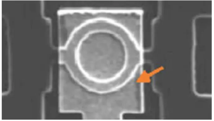
The first quantum rings were fabricated from normal metals [4, 63]. Later, due to the de-velopment of semiconductor nanotechnology, it became possible to prepare quantum rings in semiconductor heterointerfaces e.g. in AlGaAs/GaAs [64–66], InGaAs/InAlAs [32] and HgTe/HgCdTe [31], by techniques such as etching [32,67], patterning by a scanning force microscope [68], or optical and electron beam lithography [31]. The usual radii of such rings range from a hundred nanometers to a few micrometers, while their usual widths range from a few tens to a few hundreds of nanometers.
Figure 2.1: Scanning electron microscope picture of a quantum ring fabricated in InGaAs/InAlAs. The radius of the ring is 340 nm, the width of the arms is 200 nm [30].
Figure 2.1 shows a scanning electron microscope picture of an experimentally realized quantum ring in InGaAs/InAlAs, with a radius of 340 nm, and an arm width of 200 nm. The ring was fabricated by electron beam lithography and electron cyclotron resonance dry etching [30].
2.1.2
The effect of magnetic field
In a quantum ring which encloses a well-defined flux Φ the conductance has a fundamental periodicity
G(Φ) =G(Φ +nΦ0), (n= 1,2,3, ...), (2.1)
as a function of the perpendicular magnetic field B(or the flux Φ =BS through the area
S enclosed by the conductor), where Φ0 = h/|e| is called the magnetic flux quantum.
This is due to the Aharonov-Bohm effect [5, 69], which shows how an electron can be influenced by the presence of a vector potential even if the external B field is exculded from the region where the electron is moving. In most of the actual experiments however, the magnetic field penetrates the arms of the ring as well as its interior so that deviations from Eq. (2.1) can occur. Since in many situations such deviations are small, at least in a limited field range, these magnetoconductance oscillations are still referred to as Aharonov-Bohm (AB) oscillations [4, 64–66].
(a) (b) B ∆φ= 2πΦ Φ0 ∆φ= 2π Φ Φ0/2
Figure 2.2: Illustration of the effect of a magnetic field in a ring geometry. (a) The phase difference between interfering trajectories responsible for the conductance oscillations with Φ0 =h/|e|periodicity
in the enclosed flux Φ. (b) The phase difference of the pair of time-reversed trajectories which lead to oscillations with Φ0/2 =h/2|e|periodicity.
The fundamental periodicity
∆ΦAB = Φ0 = h
|e| (2.2)
in the magnetic flux is caused by the interference between trajectories which make a half-revolution around the ring, as shown in Fig. 2.2(a). The first harmonic oscillation, which pertains to the periodicity
∆ΦAAS=
Φ0
2 =
h
2|e|, (2.3)
results from interference after one complete revolution, as shown in Fig. 2.2(b). The main difference between these two types of oscillations is that in non-ideally ballistic samples, the phase of the one with h/|e| periodicity (2.2) is not fixed relative to zero magnetic field, it is sample-specific. The magnitude of this phase depends on the microscopic details of the impurity configuration. On the other hand, as the oscillations with h/2|e|
periodicity (2.3) arise from the interference of trajectories that make a full revolution in the ring, they always result in a conductance minimum at B = 0, independently of the sample. Consequently, in a geometry with many rings in series (or in parallel) the h/|e|
oscillations average out, but the h/2|e| oscillations remain [70]. The oscillations with
h/2|e| periodicity are often referred to as Al’tshuler-Aronov-Spivak (AAS) [63, 71, 72] oscillations, as these authors were the first to suggest that such oscillations should survive when conductors are disordered. Such conductance oscillations have been observed in metal cylinders [73, 74] and honeycomb networks [75, 76] as well as square loop and ring arrays fabricated in semiconductor heterostructures [32, 77].
2.1.3
Spin-dependent interference
As we have mentioned in Section 1.6, in certain heterostructures spin-orbit interaction is present at the heterointerface as a result of the inversion asymmetry of the bulk crystal
(Dresselhaus coupling), or of the asymmetry of the confining potential in the growth direction (Rashba coupling), or both. It was found that in most of the cases the dominant contribution comes from the Rashba term [57,58,78]. Additionally, this type of spin-orbit interaction is tunable with external gate electrodes [23,24], which makes it very attractive for applications in spintronics [6, 8, 9, 79, 80].
v v
Beff
Beff
Figure 2.3: Quantum ring with Rashba spin-orbit interaction [81]. The electric field originating from the asymmetric confinement potential is perpendicular to the plane of the heterointerface, where the ring is frabricated. From the rest frame of the electron there is an effective magnetic field in the plane of the interface, perpendicular to the direction of movement. The precession angles in the left and right branches are different, leading to spin-dependent interference.
If the electron is restricted to move on a ring within the heterointerface, where Rashba-type spin-orbit interaction is present – as suggested by Nitta et al. [29, 81] – then the interference will be spin dependent as a function of the external gate voltage that is applied by a gate electrode which covers the ring. This can most easily be understood if we look at the effect of spin-orbit coupling from the rest frame of the electron (see Fig. 2.3). As a result of the asymmetric confinement potential there is an electric field perpendicular to the heterointerface. The electron sees this field as an effective magnetic field Beff that is parallel to the plane of the interface (perpendicular to the electric field)
and perpendicular to the direction of its movement, consequently, its spin will precess around it with a rate that depends on the strength of the Rashba coupling α. Since the direction of the magnetic field seen by the electron is different in every point of the ring (as the direction of the velocity is always tangential) the phases acquired in the left and right arms of the ring are not the same: they have opposite signs because the precession orientation is opposite. This leads to the oscillation of the conductance as a function of the external gate voltage (Rashba coupling strength), which has been verified by experiments with single rings [31] and ring arrays [32, 33].
2.2
Model of a quantum ring with elastic scatterers
We have discussed in Section 1.4 that a scatterer placed in the arm of the ring (or the local application of a gate that affects the properties of one arm) may introduce phase
shifts in the electron wave function and change drastically the position and/or amplitude of the Aharonov-Bohm oscillations [31, 67, 82–85]. The general one-dimensional model of quantum rings we present here, which was introduced by B¨uttiker et al. [62], is able to take into account such elastic scatterers in the arms of the ring as well as in the junctions, thereby describing the imperfectness of the coupling between the current-carrying leads and the ring. We will use this model in Section 3 to describe asymmetric injection into the arms of the ring.
In order to describe elastic scattering in the arms of the ring, the model uses – instead of a potential V (x) – a transfer matrix t [86], which relates the amplitudes βin, βout of
the wave function to the left of the scatterer, to the amplitudes ˜βout, ˜βin to the right of
the scatterer (see Fig. 2.4)
t à βin βout ! = à ˜ βout ˜ βin ! . (2.4)
By taking into account the conservation of probability and time reversal symmetry [87,88],
tis given by t= Ã 1 t∗ −r ∗ t∗ −r t 1t ! , (2.5) where t=pTseiχ (2.6)
is the transmission amplitude with Ts being the transmission probability through the
scatterer, and χ the phase change in the transmitted wave.
βin βout ˜ βout ˜ βin
Figure 2.4: Schematic representation of the potentialV (x) of the scatterer.
An incoming wave from the left of the scatterer of amplitude 1 gives rise to a reflected wave with amplitude
r=e−iπ2
p
Rseiχeiχa, (2.7)
whereRs = 1−Ts is the reflection probability andχais a possible additional phase
differ-ence between the transmitted and reflected amplitudes (note that in case of a symmetric potential χa= 0). For an incoming wave to the right of the scatterer,
r0 =e−iπ2
p
Rseiχe−iχa (2.8)
scattered on more scatterers in series, one may also determine a transfer matrix of the form (2.5), which relates the amplitudes on the left of the scatterers to the amplitudes on their right, thus it is enough to consider one transfer matrix in each arm of the ring.
2.2.1
Closed ring with Aharonov-Bohm flux
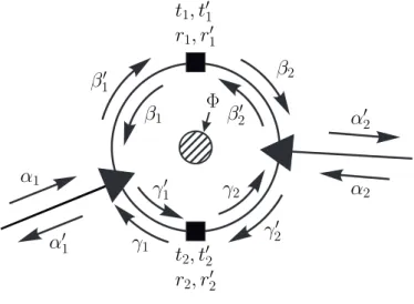
Let us consider the ring, shown in Fig. 2.5, which encircles an Aharonov-Bohm flux Φ (i.e., the magnetic field is zero in the ring). Let us assume that there are two scatterers in the ring, with transfer matrices denoted byt1 andt2. These transfer matrices give the
amplitudes of the wave functions to the right of the scatterers in terms of the amplitudes of the wave functions to the left of the scatterers. If we denote the transfer matrix which yields the amplitudes to the left of the scatterer in terms of the amplitudes to the right by t0
2, the two transfer matrices give rise to the combined scatterer t=t02t1.
t1, t0 1 r1, r0 1 t2, t0 2 r2, r0 2 Φ β0 1 β1 β20 β2
Figure 2.5: Closed ring with two elastic scatterers (denoted by the black squares) in the presence of an Aharonov-Bohm flux Φ.
As we follow the wave function around the ring, its phase changes by 2θ = 2πΦ/Φ0.
Therefore we can describe this closed ring with the following equation
£ t0 2t1−e2iθ ¤Ãβ0 1 β1 ! = 0, (2.9)
which has nontrivial solutions only if
det£t02t1 −e2iθ
¤
= 0. (2.10)
This is the eigenvalue equation of the closed ring. If we consider two equal scatterers
t1 =t2 =
√
Tseiχ, r1 =r2 = r10 =r02 =e−i
π
2√Rseiχ, where bothχ and Ts are functions of
the energy, then, Eq. (2.10) leads to
from which, for a fixed value ofθ, the discrete eigenenergies En of the closed ring can be
determined. We note that when no scattering takes place in the arms of the ring, i.e.,
Ts = 1, then the phase χis simply the geometrical phase, and the energy E is related to
it by χ=√2m∗Eρπ/~with ρ being the radius of the ring.
2.2.2
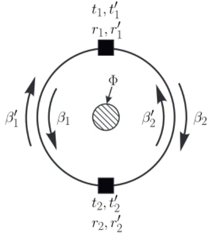
The scattering matrix method to couple leads to the ring
Now let us consider the case, when leads are attached to the ring. In the model of Ref. [62], at a junction of a lead with the ring (shown by the black triangles in Fig. 2.6), the three outgoing waves with amplitudes (α0, β0, γ0) are related to the three incoming waves (α, β, γ) by a scattering matrix S:
−
→α0 =S−→α . (2.12)
Current conservation implies that S is unitary, and time-reversal invariance implies, fur-thermore, that S∗ = S−1 [87, 88]. Consequently, the scattering matrix S has to be

![Figure 1.4 shows the measured longitudinal voltage V x and transverse voltage V H for a modulation-doped GaAs sample using a rectangular Hall bar with W = 0.38 mm and L = 1 mm and a current of I = 25.5 µA [43]](https://thumb-us.123doks.com/thumbv2/123dok_us/682429.2583153/19.892.287.630.539.799/figure-measured-longitudinal-voltage-transverse-voltage-modulation-rectangular.webp)