POUR L'OBTENTION DU GRADE DE DOCTEUR ÈS SCIENCES
acceptée sur proposition du jury: Prof. Y. Leblebici, président du jury
Prof. A. P. Burg, Prof. D. Atienza Alonso, directeurs de thèse Prof. A. Chattopadhyay, rapporteur
Prof. G. Karakonstantis, rapporteur Prof. L. Benini, rapporteur
Microarchitectural Low-Power Design Techniques for
Embedded Microprocessors
THÈSE N
O7168 (2016)
ÉCOLE POLYTECHNIQUE FÉDÉRALE DE LAUSANNE
PRÉSENTÉE LE 11 NOVEMBRE 2016
À LA FACULTÉ DES SCIENCES ET TECHNIQUES DE L'INGÉNIEUR LABORATOIRE DE CIRCUITS POUR TÉLÉCOMMUNICATIONS
PROGRAMME DOCTORAL EN GÉNIE ÉLECTRIQUE
Suisse PAR
Acknowledgements
I would like to express my gratitude to my thesis advisor Prof. Andreas Burg for giving me the opportunity to work together on such interesting topics throughout my PhD time, and for creating a supportive work environment in his laboratory. I am very grateful for our many technical discussions from which I learned a lot over the years regarding all aspects of engineering, first at ETH during my master studies and then later at EPFL. Moreover, I thank him for always having an open ear and that he was always available, whatever the problem or question, especially during important times.
I acknowledge my co-advisor Prof. David Atienza for enabling the good cooperation between his laboratory (ESL) and the Telecommunications Circuits Laboratory (TCL), when I first arrived at EPFL and during the early time of my PhD. Prof. Luca Benini, Prof. Anupam Chat-topadhyay, and Prof. Georgios Karakonstantis I would like to thank for being the examiners on my thesis defense jury, and Prof. Yusuf Leblebici for taking the role as the jury president. I want to thank Ahmed Dogan from ESL for the fruitful cooperation during the first years of my PhD, building and researching architectures for biomedical signal processing. My thanks also go to Oskar Andersson for his support with the sub-threshold characterization of TamaRISC-CS, and Pascal Meinerzhagen who generously provided the sub-threshold capable memories for the design. I am grateful to Frank Gürkaynak for our discussions and his help on the cores with SHA-3 ISEs. For their contributions to the LISA model of the OpenRISC and its extensions for fault injection, I would like to extend my thanks to Lai Wang and Zheng Wang, respectively. I am particularly grateful to team DynOR (Andrea Bonetti, Adam Teman, Christoph Müller, and Lorenz Schmid) for all their efforts and extraordinary contributions to the successful design and measurement of our first test chip in 28 nm FD-SOI. This project would not have been possible without them.
During my time at EPFL I had the pleasure to work in a wonderful environment. I was lucky to meet many terrific people over the years and had a number of great colleagues, who especially were always up for fun activities inside as well as outside the lab, which made my stay at TCL that much more enjoyable. I will take many fond memories of this time with me, from the many culinary adventures of various kinds to great nature excursions, or just the funniest discussions that we had in the office. I am very happy to be able to call them my friends: Adi Teman, Alexios Balatsoukas Stimming, Andrea Bonetti, Andrew Austin, Christian Senning, Christoph Müller, Filippo Borlenghi, Georgios Karakonstantis, Kynthia Chamilothori, Lorenz Schmid, Maitane Barrenetxea, Nicholas Preyss, Orion Afisiadis, Pablo Garcia, Pascal Giard, Pascal Meinerzhagen, Pavle Belanovic, Reza Ghanaatian, Rubén Braojos, Shrikanth Ganapathy.
Finally, I want to thank my family for all their support over the years and for always believing in my goals, which helped me immensely during all my education. I also want to express my deepest gratitude to my girlfriend Sandra for all her love and her continuous support, which always kept me going through the last years of this journey.
Abstract
Over the last two decades, embedded processing has become omnipresent in all forms of elec-tronic devices in order to provide increasingly complex features and richer user experiences. There is moreover a strong trend towards wireless, battery-powered, portable embedded systems which have to operate under stringent energy constraints. Consequently, low power consumption and high energy efficiency have emerged as the two key criteria for embedded microprocessor design. While technology scaling continues to provide improvements in both performance and power, architectural design has become equally if not even more impor-tant to meet desired performance requirements with severely limited power budgets. In this thesis we present a range of microarchitectural low-power design techniques which enable the increase of performance for embedded microprocessors and/or the reduction of energy consumption, e.g., through voltage scaling.
A popular technique for the improvement of processor performance in application-specific systems/scenarios are instruction set extensions (ISEs). In the context of cryptographic applications, we explore the effectiveness of ISEs for a range of different cryptographic hash functions on a microcontroller architecture. Specifically, we demonstrate the effectiveness of light-weight ISEs based on lookup table integration and microcoded instructions using finite state machines for operand and address generation. The proposed ISE concepts are evaluated on the PIC24 architecture (a 16-bit microcontroller) with the final round SHA-3 candidate hash algorithms.
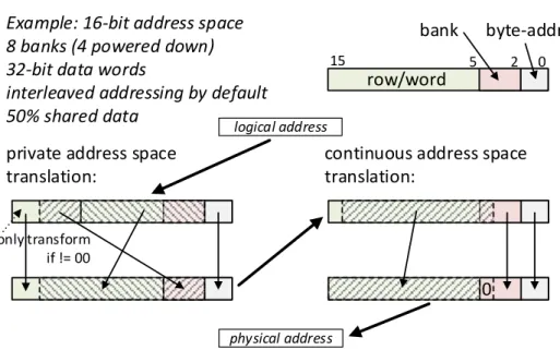
On-node processing in autonomous wireless sensor node devices requires deeply embedded cores with extremely low power consumption. To address this need, we present TamaRISC, a custom-designed ISA with a corresponding ultra-low-power microarchitecture implemen-tation. The TamaRISC architecture is employed in conjunction with an ISE and standard cell memories to design a sub-threshold capable processor system targeted at compressed sensing applications. For a case study of electrocardiogram (ECG) signal compression we show that significant power savings of more than 11x over the state of the art for programmable architectures are possible. We furthermore employ TamaRISC in a hybrid SIMD/MIMD multi-core architecture targeted at biomedical signal processing applications with moderate to high processing requirements (>1 MOPS). A range of different microarchitectural techniques for efficient memory organization are presented, which can provide significant energy savings of more than 50%. Specifically, we introduce a configurable data memory mapping technique for private and shared access, as well as instruction broadcast together with synchronized code execution based on checkpointing.
We then study an inherent suboptimality due to the worst-case design principle in syn-chronous circuits, and introduce the concept of dynamic timing margins. We show that dynamic timing margins exist in microprocessor circuits, and that these margins are to a large extent state-dependent and that they are correlated to the sequences of instruction types which are executed within the processor pipeline. To perform this analysis we propose a circuit/processor characterization flow and tool called dynamic timing analysis. Moreover, this flow is employed in order to devise a high-level instruction set simulation environment for impact-evaluation of timing errors on application performance. The presented approach improves the state of the art significantly in terms of simulation accuracy through the use of statistical fault injection.
The dynamic timing margins in microprocessors are then systematically exploited for through-put improvements or energy reductions via our proposed instruction-based dynamic clock adjustment (DCA) technique. To this end, we introduce a 32-bit microprocessor with cycle-by-cycle dynamic clock adjustment. The microarchitecture of the employed OpenRISC core comprises a 6-stage pipeline, and its implementation is specifically tuned for DCA. Besides a comprehensive design flow and simulation environment for evaluation of the DCA approach, we additionally present a silicon prototype of our DCA-enabled microarchitecture fabricated in 28 nm FD-SOI CMOS. The fully operational test chip includes a suitable clock generation unit which allows for cycle-by-cycle clock adjustment over a wide range with fine granularity at frequencies exceeding 1 GHz. Measurement results of speedups and power reductions through voltage scaling are provided.
Keywords: low-power design, microarchitecture, instruction set architecture, instruction
set extensions, ultra-low-power embedded processor, microcontroller, ASIC, VLSI design, sub-threshold operation, multi-core architecture, sensor nodes, biomedical signal process-ing, cryptographic hash functions, SHA-3, compressed sensprocess-ing, dynamic timing margins, dynamic timing analysis, dynamic clock adjustment, timing errors, statistical fault injection, approximate computing, OpenRISC
Zusammenfassung
In den letzten zwei Jahrzehnten ist eingebettet Datenverarbeitung in jeglichen Formen von Elektronik allgegenwärtig geworden, um immer komplexere Funktionen und reichere User Ex-periences zur Verfügung zu stellen. Es gibt zudem einen starken Trend zu drahtlosen, batterie-betriebenen, tragbaren eingebetteten Systemen, die unter strengen Energieeinschränkungen arbeiten müssen. Folglich haben sich niedriger Energieverbrauch und hohe Energieeffizi-enz als die beiden Schlüsselkriterien für eingebetteten Prozessorentwurf entwickelt. Obwohl CMOS-Technologiefortschritte weiterhin Verbesserungen in puncto Rechenleistung und Ener-gieverbrauch ermöglichen, ist Architekturentwurf mittlerweile gleichbedeutend oder sogar noch bedeutender geworden um gewünschte Rechenleistungsanforderungen mit stark be-schränkten Energiebudgets zu erfüllen. In dieser Dissertation präsentieren wir eine Reihe von mikroarchitekturellen energiesparenden Entwurfstechniken, die erhöhte Leistung für einge-bettete Mikroprozessoren und/oder die Verringerung des Energieverbrauchs, zum Beispiel durch Spannungsskalierung, ermöglichen.
Eine beliebte Technik zur Verbesserung der Prozessorleistung in anwendungsspezifischen Sy-stemen/Szenarien sind Befehlssatzerweiterungen (BSE). Im Rahmen von kryptographischen Anwendungen untersuchen wir die Effektivität von BSE für eine Reihe von verschiedenen kryptographischen Hash-Funktionen auf einer Mikrocontroller-Architektur. Insbesondere zeigen wir die Effektivität von leichten/einfachen BSE basierend auf Integration von Um-setzungstabellen und mikrocodierten Instruktionen unter Verwendung von endlichen Zu-standsautomaten für die Generierung von Operanden und Adressen. Die vorgeschlagenen BSE-Konzepte werden auf der PIC24 Architektur (ein 16-bit Mikrocontroller) zusammen mit den SHA-3 Hash-Algorithmus-Kandidaten der letzten Runde ausgewertet.
Datenverarbeitung in autonomen Funksensorknoten erfordert tief eingebettete Rechenkerne mit extrem niedrigem Stromverbrauch. Um diesem Bedarf zu begegnen, stellen wir Tama-RISC vor, eine speziell entworfene Befehlssatzarchitektur mit einer dazugehörigen ultra-energiesparenden Mikroarchitektur-Umsetzung. Die TamaRISC Architektur wird in Verbin-dung mit einer BSE und Standardzellen-Speicher verwendet, um ein Prozessorsystem für Anwendungen basierend auf komprimierter Abtastung zu entwerfen, welches unterhalb der Schwellenspannung betrieben werden kann. Für eine Fallstudie von Elektrokardiogramm (EKG) Signalkompression zeigen wir, dass erhebliche Energieeinsparungen von mehr als 11x über den Stand der Technik für programmierbare Architekturen möglich sind. Wir verwenden außerdem TamaRISC in einer hybriden SIMD/MIMD Mehrkernarchitektur welche für bio-medizinischen Signalverarbeitungsanwendungen mit mittleren bis hohen Anforderungen an
die Verarbeitung (>1 MOPS) entworfen ist. Eine Reihe von unterschiedlichen Mikroarchitek-turtechniken für eine effiziente Speicherorganisation werden vorgestellt, welche erhebliche Energieeinsparungen von mehr als 50% ermöglichen. Insbesondere stellen wir eine Technik für konfigurierbare Speicher-Address-Übersetzung für privaten und gemeinsamen Zugriff, sowie Befehlsübertragungen zusammen mit synchronisierter Codeausführung auf Basis von Programmhaltepunkten.
Wir untersuchen dann eine inhärente Suboptimalität aufgrund des Schlimmstfall-Entwurfs-prinzips von synchronen Schaltungen, und führen das Konzept der dynamischen Zeit-Margen ein. Wir zeigen, dass dynamische Zeit-Margen in Mikroprozessorschaltungen vorhanden sind, und dass diese Margen zu einem großen Teil zustandsabhängig sind, und dass sie zu den Sequenzen von Befehlstypen korreliert sind, die innerhalb der Prozessor-Pipeline ausgeführt werden. Zur Durchführung dieser Analyse schlagen wir eine Schaltung/Prozessor-Charakterisierungs-Methodik und Werkzeug namens dynamische Zeit-Analyse vor. Darüber hinaus verwenden wir diese Methodik, um eine High-Level-Befehlssatz-Simulationsumgebung zu entwickeln für die Evaluation der Auswirkung von zeitlichen Fehlern auf die Anwendungs-leistung. Der vorgestellte Ansatz verbessert den Stand der Technik im Hinblick auf die Simula-tionsgenauigkeit durch den Einsatz von statistischer Fehlerinjektion.
Die dynamischen Zeit-Margen in Mikroprozessoren werden dann für die Durchsatzsteige-rung oder für EnergieeinspaDurchsatzsteige-rungen durch unsere vorgeschlagene befehlsbasierte dynamische Taktanpassung (DT) systematisch genutzt. Zu diesem Zweck stellen wir einen 32-bit Mikropro-zessor mit Zyklus-zu-Zyklus DT vor. Die Mikroarchitektur des eingesetzten OpenRISC Kerns besteht aus einer 6-stufigen Pipeline und ihre Implementierung ist für DT speziell abgestimmt. Neben einer umfassenden Entwurfsmethodik und Simulationsumgebung für die Evaluierung des DT Ansatzes, stellen wir zusätzlich einen Silizium Prototyp unserer DT-fähigen Mikroar-chitektur vor, welcher in 28 nm FD-SOI CMOS hergestellt wurde. Der voll funktionsfähige Testchip beinhaltet eine geeignete Takterzeugungseinheit, die eine Zyklus-zu-Zyklus Taktan-passung über einen weiten Bereich mit feiner Granularität ermöglicht, bei Frequenzen von mehr als 1 GHz. Die Messergebnisse der Beschleunigungen und der Energiereduzierungen durch Spannungsskalierung werden zusätzlich vorgestellt.
Stichwörter:energiesparender Entwurf, Mikroarchitektur, Befehlssatzarchitektur,
Befehlssat-zerweiterungen, ultra-energiesparender eingebetteter Prozessor, Mikrocontroller, ASIC, VLSI Entwurf, unter-Schwellenspannung Betrieb, Mehrkernarchitektur, Sensorknoten, biomedizini-sche Signalverarbeitung, kryptographibiomedizini-sche Hashfunktionen, SHA-3, komprimierte Abtastung, dynamische Zeit-Margen, dynamische Zeitanalyse, dynamische Taktsignalanpassung, zeitli-che Fehler, statistiszeitli-che Fehlerinjektion, approximierende Datenverarbeitung, OpenRISC
Contents
Acknowledgements i
Abstract (English/German) iii
1 Introduction 1
1.1 CMOS Power and Energy Consumption . . . 5
1.2 Supply Voltage Scaling . . . 7
1.3 Contributions . . . 13
1.4 Thesis Outline . . . 16
1.5 Selected Publications . . . 17
1.6 Third-Party Contributions . . . 19
2 Microcontroller Architecture Enhancements for Cryptographic Applications 21 2.1 Applications: SHA-3 Selection Competition Algorithms . . . 22
2.1.1 Principles of Cryptographic Hash Functions . . . 23
2.1.2 SHA-3 Candidate Algorithms . . . 25
2.2 Embedded Microcontroller Architecture (PIC24) . . . 28
2.2.1 Instruction Set Architecture . . . 28
2.2.2 Microarchitecture . . . 30
2.3 Performance Metrics . . . 32
2.4 Baseline Performance on PIC24 . . . 33
2.4.1 Baseline Implementations . . . 33
2.4.2 Performance Results and Comparison . . . 39
2.5 Architecture Enhancements Through Instruction Set Extensions . . . 40
2.5.1 ISE Design Flow . . . 41
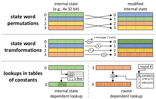
2.5.2 ISE Types for Cryptographic Hash Functions . . . 43
2.5.3 Algorithm-Specific ISE of SHA-3 Finalists . . . 49
2.5.3.1 BLAKE ISE . . . 50
2.5.3.2 Grøstl ISE . . . 52
2.5.3.3 JH ISE . . . 54
2.5.3.4 Keccak ISE . . . 55
2.5.3.5 Skein ISE . . . 56
2.6 Performance on PIC24 with ISEs . . . 57
2.6.2 Memory Consumption . . . 59
2.6.3 Hardware Overhead . . . 60
2.6.4 Energy Considerations . . . 62
3 Microprocessor Design for Deeply Embedded Ultra-Low-Power Processing 65 3.1 TamaRISC: A 16-bit Core for ULP Applications . . . 66
3.1.1 Instruction Set Architecture . . . 67
3.1.2 Microarchitecture . . . 69
3.1.3 Implementation & Evaluation Flow . . . 70
3.1.4 Software Toolchain and Real-Time OS Support . . . 72
3.2 TamaRISC-CS: A Sub-Threshold ULP Processor for Compressed Sensing . . . . 74
3.2.1 Compressed Sensing . . . 76
3.2.1.1 Reduced Complexity Compression Algorithm . . . 76
3.2.1.2 Pseudorandom Number Generation . . . 77
3.2.1.3 Index Sequence Implementations . . . 78
3.2.2 Instruction Set Extension for CS . . . 79
3.2.3 Sub-VTMemories . . . 81
3.2.4 Power and Performance Results . . . 83
3.2.4.1 Synthesis Strategy and Sub-VTEnergy Profiling . . . 83
3.2.4.2 Implementation and Simulation Results . . . 85
3.2.4.3 Case Study: CS-Based ECG Signal Compression . . . 88
3.3 Comparison with State of the Art . . . 92
3.4 Multi-Core Processing . . . 95
3.4.1 Comparison of Single-Core and Multi-Core Processing . . . 95
3.4.2 Efficient Memory Organization . . . 97
3.4.2.1 Configurable Data Memory Mapping . . . 98
3.4.2.2 Data and Instruction Broadcast . . . 101
3.4.2.3 Synchronized Code Execution . . . 104
4 Dynamic Timing Margins in Embedded Microprocessors 107 4.1 Timing Margins in Synchronous Circuits . . . 108
4.1.1 Variations, Guardbanding, and Mitigation Techniques . . . 109
4.1.2 State-Dependent Dynamic Timing Margins . . . 113
4.1.3 Dynamic Timing Analysis . . . 116
4.2 Dynamic Timing Analysis for Microprocessors . . . 119
4.3 Characterization of Application Behavior under Timing Errors due to Frequency-and/or Voltage-Over-Scaling . . . 123
4.3.1 Case Study . . . 125
4.3.1.1 Hardware Processor Core . . . 125
4.3.1.2 Instruction Set Simulator with Fault Injection . . . 126
4.3.1.3 Software Benchmarks . . . 127
4.3.2 Modeling of Timing Errors . . . 129
Contents
4.3.2.2 Static Timing Based FI . . . 130
4.3.2.3 Supply Voltage Noise . . . 132
4.3.2.4 Proposed Dynamic Timing Statistical FI . . . 133
4.3.3 Application of Statistical FI . . . 135
4.3.3.1 Instruction Characterization . . . 135
4.3.3.2 Impact of Frequency, Voltage, and Noise . . . 136
4.3.3.3 Performance Comparison of Benchmarks . . . 138
4.3.3.4 Error vs. Power Consumption Trade-Off . . . 140
5 A Microprocessor with Cycle-By-Cycle Dynamic Clock Adjustment 143 5.1 Instruction-Based Dynamic Clock Adjustment . . . 144
5.1.1 Related Work . . . 144
5.1.2 DCA Concept . . . 146
5.1.3 Design Flow and Evaluation Environment . . . 148
5.1.3.1 Implementation . . . 148
5.1.3.2 Characterization . . . 149
5.1.3.3 DCA Evaluation . . . 151
5.2 DCA Case Study Based on Instruction Set Simulation . . . 151
5.2.1 OpenRISC Microarchitecture, Optimization, and Implementation . . . . 152
5.2.2 Performance Evaluation Environment . . . 154
5.2.3 Characterization and Performance Results . . . 155
5.2.3.1 Dynamic Timing Analysis of OpenRISC . . . 155
5.2.3.2 Performance and Power . . . 158
5.3 DynOR Hardware Architecture . . . 160
5.3.1 Chip Architecture . . . 160
5.3.2 Dynamic Clock Adjustment Module . . . 161
5.3.3 Clock Generation Module . . . 162
5.4 DynOR Test-Chip . . . 164
5.4.1 Implementation . . . 164
5.4.2 Measurement Setup . . . 166
5.4.3 DCA LUT Calibration . . . 168
5.5 Measurement Results . . . 172
5.5.1 Speedup . . . 174
5.5.2 Power Reduction . . . 175
5.5.3 Comparison . . . 176
6 Conclusions & Outlook 179
Bibliography 185
Glossary 201
List of Tables 213
List of Publications 215
1
Introduction
Embedded processing has arguably evolved as the predominant form of computing over the past two decades. Any form of electronics produced today typically integrates some form of embedded processor, covering every kind of application imaginable, from consumer to industrial, over medical to automotive. While the field of embedded systems has been dominated in the past by small microcontrollers focused on simple control tasks with very little processing power, the evolution of embedded computing has today given rise to complex systems-on-chip (SoCs) which provide very high processing capabilities under the most stringent energy and cost constraints.
With the advances in ubiquitous and pervasive computing [Wei99, Sat01, HB01, ECPS02], computing and specifically data processing now occurs already in many objects around us, anywhere at anytime. In recent years this development has accelerated significantly with the conception of the internet of things (IoT) and similar concepts, which aim to not only locally connect all these objects and devices, but to interconnect them on a global scale to enable new applications and ways of computing.
A model for the internet of things is illustrated in Figure 1.1 [IBM14]. The “things” or end devices provide often sensors and/or actuators and always comprise some form of processing, performed on one or multiple embedded microprocessor(s). The devices connect typically wirelessly to a local network, which can consist of multiple layers and intermediary larger nodes, again requiring embedded processing capabilities. These local networks integrate with the internet, which allows for the end devices to be controllable via data center driven applications. The end user typically interacts with the end devices or rather with the whole application or service, which encompasses the end devices, via a personal controlling device such as a smartphone or tablet.
Wireless sensor nodes are one of the most prominent types of end devices in the IoT con-text. Such nodes combine sensing and processing capabilities in a constantly shrinking form factor, and are comprised of an embedded low-power processor subsystem, a sen-sor with an analog to digital converter, a radio, as well as a battery. A prime example for
Chapter 1. Introduction
Arguably, the defining characteristic of a “thing” is the ability to remotely view and control it, often from a smart mobile device. “Things” can also send telemetry to a central collection and analytics point. A cloud service often provides the
repository and access control between the “thing” and its controller.
Let’s dissect a few “things” and see how they fit the model. Local network
Global network
Graphic 1. IBM model for the Internet of Things
IBM model for the Internet of Things
Controlling device Cloud service
“Things” can be remotely controlled or viewed, and they can send telemetry for analysis.
Smartphones, tablets and other smart devices can control all types of “things.”
Cloud services provide the repository and access control between the “thing” and its controller.
Most “things” connect to the Internet, except for power grids or classified government systems.
This may be a controller area network (CAN) in connected cars, a local network in homes, etc.
{
{
{
{
{
ThingsFigure 1.1 – Model for the internet of things [IBM14], with embedded microprocessors inte-grated as part of the end devices/“things”, the intermediary nodes in the local network, and the controlling devices of the end users.
an application of wireless sensor nodes are wireless body sensor networks (WBSNs). WB-SNs are very successfully employed in the domain of healthcare and fitness, where they provide a low-cost solution for continuous monitoring and logging of a person’s vital parame-ters [RMC05, CLC+09, YY10, KMKA11]. An example for a WBSN-based system as it is used in a
typical healthcare monitoring application is given in Figure 1.2 [CCHL12]. Here, the WBSN provides personal monitoring capabilities for the medical conditions of patients, which allows for example the implementation of automated warning systems, and can trigger emergency interventions in urgent cases. To allow for such a warning and detection system to operate efficiently, the microcontroller unit (MCU) in the end node has to provide appropriate capa-bilities for processing of the sensor data, since transmission of raw sensor data is normally too costly in terms of energy consumption [MKAV11, Dog13]. As illustrated in Figure 1.2 such a wireless sensor node can comprise a wide variety of different sensors, even with multiple channels. In this example, the temperature, blood pressure, and heartbeat of the patient are monitored via the wireless sensor node.
One of the most important aspects of such sensor nodes is that their operation is largely autonomous and battery-driven. Although there is extensive research into energy harvesting
Figure 1.2 – Wireless body sensor network (WBSN) system for hospital and healthcare moni-toring applications [CCHL12].
techniques for fully autonomous operation of sensing devices in general, the amount of energy and especially instantaneously available power that can be provided is overall still quite limited [PS05, MYR+08, GWZ13]. Wireless sensor nodes hence require highest energy
efficiency on a complete system/device level in order to provide adequate operation time considering their limited battery capacity.
The need for deeply embedded processing is growing due to more and more complex tasks required by the applications that are performed on such devices. Moreover, especially because of the mentioned limitation in terms of data volume that can be transmitted over an integrated radio on a tight power budget, on-node (signal) processing is becoming increasingly necessary. However, significant gains in terms of energy efficiency and in turn battery lifetime can only be achieved through low-power microprocessor/microcontroller subsystems, which are executing the required signal processing algorithms.
The system diagram of a state-of-the-art embedded subsystem for IoT applications, integrat-ing an ARM Cortex-M microprocessor is depicted in Figure 1.3 [ARM16]. The system includes, besides the processing core, a light-weight bus interconnect that provides access to memory controllers as well as to a radio and other peripherals. As an example for a microarchitectural measure to bring down energy consumption, the system uses a flash cache since any accesses that are made to the embedded flash memory are very energy-intensive. Furthermore, such systems comprise a power management unit, which allows the circuit to better operate accord-ing to the current requirements of the application and to save power by employaccord-ing techniques such as clock gating or power gating for parts of the circuit which are temporarily not utilized. Another popular option for power optimization provided by a power management unit, is the adjustment of the different clock frequencies of the various components on the to their
Figure 1.3 – System diagram of an exemplary state-of-the-art embedded subsystem for IoT applications, integrating a Cortex-M microprocessor [ARM16].
current throughput needs. Additionally, especially in more complex SoC designs of recent years, supply voltages can often be adjusted through the use of on-chip regulators to achieve very low power consumption.
Highest energy efficiency is however not only required for deeply embedded IoT end node type devices with their severely limited battery capacities. Also devices incorporating larger SoCs for embedded and mobile applications operate under stringent energy constraints, often with total system power budgets of a few hundred mW to one W, even for computing scenarios with high performance requirements. This is not only due to battery limitations, but also increasingly due to thermal limits that have to be met for high performance hand-held devices with very small form factors, imposing strong constraints on the employed heat management and cooling solutions [SA14, SVC15].
As a consequence, there is an increasing need for very high energy efficiency in embedded microprocessors, over the full processing performance and application spectrum. Energy efficiency has become the most important and driving design constraint in the further evo-lution of such systems, even over other important aspects such as silicon area or maximum achievable clock frequency. There are many layers in the computing stack of a programmable architecture, which can all contribute significantly to the power consumption of the complete system. While choosing the appropriate algorithm for the given task at hand is of course paramount, lower layers of the stack can still provide significant improvements after optimiza-tions on the higher, more abstract layers have been exploited to their full potential.
In this thesis the focus lies on microarchitectural design techniques and optimizations, which are on the boundary between the instruction set architecture of a microprocessor — i.e., the fixed contract between the programmer/software and the hardware — and the physical
1.1. CMOS Power and Energy Consumption
hardware implementation of the circuit. The microarchitectural improvements especially enable energy efficient and/or low-power operation, when they are combined with supply voltage scaling, a key technique for lowering the power consumption of digital circuits. The following two sections provide an overview of the contributing factors for the power consumption in a digital complementary metal–oxide–semiconductor (CMOS) circuit, and then introduce the general benefits and challenges stemming from voltage scaling for micro-processor circuits.
1.1 CMOS Power and Energy Consumption
The power consumption in watts [W] of a circuit denotes the amount of energy in joules [J] that is dissipated per second.1 While absolute power numbers for a given state of a system (active, idle, sleep, etc.) are useful on a full system level, note that this measure usually does not relate to the performance of the circuit since it does not reflect the amount of computational work or processing that is performed for the given power consumption. Especially from an architectural design point of view it is hence often more useful to consider the amount of energy used per computational operation or per processed data item [Kae08], which is often also referred to as the energy efficiency. Thus, in the following we focus on the different energy components that get dissipated in a CMOS circuit and relate these quantities to the power consumptionP, with the following simple equation:
P=fcEc. (1.1)
Here, fc denotes the computation rate, which for a single-edge-triggered digital circuit is
normally equivalent to the clock frequencyfclkat which the circuit operates, whileEcstands
for the total energy dissipated per computation cycle (or rather its average over many cycles). Echas two main components, the active energyEacti ve, which is dissipated due to switching
of the circuit, and the static energyEst ati c, which is constantly dissipated, as long as the circuit
is powered, i.e., connected to a supply voltage. This means thatEacti veis only dissipated when
the circuit receives a clock2, whileEst ati cis also consumed during phases where the clock is
not active.
Ec=Eacti ve+Est ati c (1.2)
The active energyEacti vecan be split up in two components, the energyEchspent on charging
1The introduction to power consumption and energy dissipation in CMOS circuits of this section is based on the
excellent explanations and observations in Chapter 9.1 of the textbook “Digital Integrated Circuit Design” [Kae08]. This includes most formulas.
2Technically, it is also possible for active energy to be dissipated when primary inputs of a circuit or module
and discharging of capacitive loads, and the energyEcrdissipated due to crossover currents.
Eacti ve=Ech+Ecr (1.3)
The static energyEst ati c also has two parts, the leakage energyEleak, and the energyEr r
consumed by driving of resistive loads.
Est ati c=Eleak+Er r (1.4)
Charging and discharging of capacitive loads (Ech) The energy that is dissipated in the
p-MOS/n-MOS transistors as thermal energy in order to either charge or discharge the capac-itive loadCk of a nodekis12CkVdd2 , with the supply voltage atVdd. Together with the node
activityαk, which indicates how many times per cycle a nodekon average switches from one
logic state to the other, we deriveEchfor the complete circuit withKdifferent nodes as:
Ech=Vdd2 K X k=1 αk 2 Ck. (1.5)
We can observe from (1.5) thatEchcan be either reduced by decreasing the total amount of
capacitance over all nodesK (e.g., via proper gate sizing), or by lowering the activitiesαk, for
example through clock gating or by avoiding as many glitches as possible during the settling phases of nodes. More important however,Echcan be significantly reduced by loweringVdd,
due to the quadratic dependence ofEchonVdd. Note that this is the key observation which
makes supply voltage down-scaling such an effective technique for power reduction [WCC06].
Crossover currents (Ecr) During the switching phase of the p- and n-network of a CMOS
gate, energy is additionally dissipated due to current that flows directly from supply to ground while for a short time both the p- and n-paths are partially conducting. The exact energy that is dissipated due to crossover/short-circuit currents depends on numerous factors. However, if transition times of gate inputs can be kept as short as possible, the contribution ofEcr
towards the total active energy is small. Furthermore,Ecris also decreased by a supply voltage
reduction, with a cubic dependency onVdd.
Leakage currents (Eleak) The major part of static power consumption typically stems from
leakage currents that occur due to the imperfections of the p- and n-MOS devices in a CMOS process. The contributors toEleakare sub-threshold conduction of channels that are turned
off, gate leakage, and leakage currents through multiple combinations of reverse-biased junctions (drain/source with bulk, and well with well/substrate). Since leakage energy is dissipated for all devices in the circuit, the total leakage energy is linearly dependent on the number of transistors (or more specifically the sum of their widths) or roughly on the overall utilized silicon area. Leakage has become an increasingly larger part of the total energy/power
1.2. Supply Voltage Scaling
consumption of circuits in more advanced bulk CMOS technology nodes (sub-65 nm), mainly due to reduced threshold voltages, which create more issues for the channel control in its off state. However, to address these problems, an increasing number of different process options for a single technology node are offered by foundries, allowing to better optimize the device performance towards the circuit requirements (low power, low leakage, high speed, etc.). In relation to voltage scaling, leakage energy becomes increasingly relevant for circuit operation near and especially below the threshold voltage (i.e., forVdd.VT). This is due to
the significantly reduced active energy dissipation at these operating points, which requires the careful management of leakage energy to achieve further energy reductions. Leakage energy exponentially depends both on the supply voltage (lowerVddreduces leakage power)
and on the threshold voltage (higherVT reduces leakage).
Driving of resistive loads (Er r) In theory, there should be no static currents flowing in
a CMOS circuit that is not switching (besides the unavoidable leakage currents), since by design there should be no direct static paths between supply and ground. However, many exceptions to this exist, involving: amplifiers (e.g., contained in memories), clock generation and conditioning subcircuits, voltage converters and regulators, on-chip pull-ups/downs, and electrostatic discharge (ESD) protection structures. For a more extensive list of examples, the reader is referred to [Kae08]. Much likeEch, which is dissipated by the charging of capacitive
loads, alsoEr r has a quadratic dependence onVdd.
1.2 Supply Voltage Scaling
Reduction of the supply voltage of a CMOS circuit has the potential to provide significant energy and power savings, as indicated by (1.5). The evolution of submicron technology nodes has hence initially delivered substantial power savings, due to technology-driven re-duction of the nominal supply voltage (mainly to avoid dielectric breakdown of thinner gate oxides [Kae08]), besides other aspects. However, about a decade ago, in deep submicron technologies below 90 nm, this trend of nominalVddreduction began to level off to around 1 V
(at 65/40 nm).3Since then we have seen an increasing usage of many different forms of voltage
scaling techniques, which aim at operating circuits belownominal Vddlevels, down to the
near- or even sub-threshold level to further reduce energy consumption. Especially the con-cept of dynamic voltage frequency scaling (DVFS) has been widely adopted by industry, which operates the circuit at fixed pairs of voltage and frequency tuned for specific usage scenarios. In more forward looking proposals DVFS is used in a closed-loop fashion, dynamically adjusting voltage and/or frequency according to detected timing violations [EKD+03, TBW+09].
However, dynamic voltage scaling has its limitations [ZBSF04] and energy gains from supply voltage scaling do not come for free since reducedVddincreases the gate delays of the circuit, 3The latest non-bulk CMOS nodes, using FinFET devices, seem to further push these limits again, with standard
therefore reducing its maximum clock frequency. In the operating region above the threshold voltageVT, the proportionality of a CMOS gate delaytpd (propagation delay) [Kae08] with
respect to the supply voltageVddis given by:
tpd∝(VCkVdd
dd−VT)α. (1.6)
Here,Ckis again the node capacitance which the output of the gate has to drive, whileαis an
empirical constant greater than 1, which depends on the specifics of the technology that is employed. For deep submicron technologiesαis typically close to 1, due to velocity saturation. WithCkandVTfixed for a given circuit implementation in a specific technology, andα≈1, we
can consider the proportionality of the clock frequency fclk=tpd1 as a function of the supply
voltageVdd:4 fclk∝C1 k− VT Ck · 1 Vdd. (1.7)
We can observe that the clock frequency is linearly dependent on the supply voltage, since the right-hand side of (1.7) grows linearly with increasingVdd(with the subtrahend of the
difference decreasing linearly, while the minuend remains constant). Furthermore, when scal-ing of the supply voltage continues below the threshold voltage, sub-threshold currents drive transistor operation, causing (1.6) and (1.7) to be not applicable anymore for this operation region. For the sub-threshold regime the delay starts to become exponentially dependent on the supply voltage, which creates a severe performance degradation for any additional savings that should be achieved in terms of power consumption.
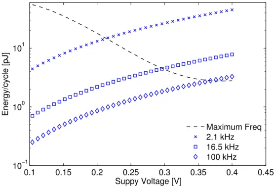
A qualitative overview and comparison of circuit power, frequency, and energy per operation as a function of supply voltage is given in Figure 1.4 [KKT13].5 The figure illustrates how
performance in terms of maximum operating frequency is degraded by 5-10x when scaling the supply voltage from the nominal operating point (VDDSTV) to an operating point that is near
the threshold voltage (VDDNTV). At the same time, power consumption is reduced by 10-50x
due to two factors: the circuit is operated at a lower frequency, so the amount of switching per second is reduced; additionally, the circuit operates at a lower supply voltage, which especially reduces active power even further according to (1.5). As a result the energy efficiency of the circuit improves by 2-5x when it is operated at near-threshold, compared to the nominal operating point in the above-threshold region. As can be seen in the frequency plot, the performance degradation starts to become exponential near the threshold voltage, actually causing an increase in the energy per operation after some point in the sub-threshold region. This is due to the leakage energy which starts to dominate over the dissipated active energy, when computation cycles become exponentially longer. The operating point with the lowest possible energy per operation, i.e., the best energy efficiency, is called the energy minimum
4For simplicity, the delayt
pdis here assumed to be the total delay of all gates on the critical path, whileCk
denotes the overall capacitance.
1.2. Supply Voltage Scaling
Unfortunately, state-of-the-art on-chip
V
DDregulation is energy inefficient,
5barely
tolerable in the energy-conscious NTC
environment.
Without addressing variation, we can’t
unlock NTC’s potential. In this article, we
confront variation by introducing an
archi-tectural model of parametric variation at
NTV. We use the model to show the
short-comings of adopting state-of-the-art STC
techniques for variation mitigation at NTV.
We also examine how to tailor variation
mit-igation to NTC, using a single-
V
DD-domain
many-core organization called EnergySmart.
Background
In this section, we cover the basics of
NTV operation and the impact of
paramet-ric variation at NTV.
NTV operation basics
For the current technology, the NTC
V
DDis about 0.5 V, while the STC
V
DDis
about 1 V. Figure 1 depicts the power,
f
,
and energy per operation as a function of
V
DD.
3,6At NTC, the energy per operation
improves by 2 to 5
over STC, at the
expense of a 5 to 10
f
degradation. As a
result, power reduces by 10 to 50
, which
enables more cores to fit into a given
power budget.
The minimum power and
energy-per-operation points fall into the subthreshold
regime (
V
DD<
V
th), where
f
degrades
signif-icantly. The STV regime accommodates the
maximum
f
, at the cost of notably higher
power and energy per operation. The NTV
regime is a sweet spot, with power savings
closer to subthreshold but with
f
closer to
STV. Away from NTV, higher
V
DDleads
to substantially higher power, and lower
V
DDto substantially lower
f
.
Impact of parametric variation at NTV
Parametric variation is the discrepancy
between the device parameters’ design
speci-fication and the actual values. It is caused by
manufacturing imperfections, and gets worse
as feature sizes shrink. Within-die (WID)
variation has a systematic and a random
component. The former is typically caused
by lithographic irregularities, while the latter
is caused by varying dopant concentrations.
A processor or memory block’s
f
of
opera-tion and power consumpopera-tion depends on
two key parameters vulnerable to variation:
V
thand effective channel length (
L
eff).
In a many-core setting, WID variation in
V
thand
L
effwidens the spread of the cores’
(and memory blocks’)
f
distributions. This
results in a lower operating
f
, because the
dis-tribution tail determines the
f
. Moreover,
WID variation in
V
thincreases the static
power consumption because devices with
lower
V
thconsume more than devices with
higher
V
thsave. The higher the variation in
V
thand
L
eff, the higher the variation in
f
and power across cores and memories.
NTV operation intensifies the
susceptibil-ity to parametric variation. As
V
DDgets close
to
V
th, the transistor’s switching speed
becomes more sensitive to variation. As a
re-sult, the timing guardband required to
toler-ate a fixed amount of
V
thvariation grows as
V
DDdecreases. This is shown in Figure 2,
from Chang et al.
2[3B2-9] mmi2013040006.3d 24/7/013 9:44 Page 7 Power log ( f ) Energy/operation VDDNTV Vth VDDSTV VDDNTV Vth VDDSTV VDDNTV Vth VDDSTV VDD VDD VDD 10–50× 5–10× 2–5×
Figure 1. Power, frequency (f), and energy per operation as a function of supply voltage (VDD).3,6At near-threshold voltage computing (NTC), the energy per operation improves by about 2 to 5 over super-threshold voltage computing (STC), at the expense of a 5 to 10fdegradation. (VDD: supply voltage;Vth: threshold voltage.)
...
7
Figure 1.4 – Qualitative overview for power, frequency (f), and energy per operation as a function of supply voltage (VDD) [KKT13, DWB+10, JKY+12], highlighting the gains from
sup-ply voltage scaling, and the induced performance degradation. Vthdenotes the threshold
voltage, VDDNTVdenotes a near-threshold operating voltage, while VDDSTVdenotes the classical
super/above-threshold operating voltage.
voltage (EMV) point. The position of the EMV relative to the threshold voltage depends on many factors, such as the employed CMOS technology and process option, but of course is also highly dependent on the architecture and circuit structure of a design, and can range from deep sub-threshold to near-threshold.
In addition to the strong performance degradation, low-voltage operation in the near-threshold regime and below gives rise to a set of problems regarding increased parametric and perfor-mance variation [DWB+10, KKT13]. For example, at near-threshold delay uncertainty due to
global process variation can increase from 30% at nominal voltage (1 V) to 400% at 400 mV supply. Together with the more severe sensitivity to temperature and supply voltage noise effects, the total performance uncertainty rises to 20x, compared to only≈1.5x at nominal voltage [DWB+10]. Moreover, near- and sub-threshold computing poses significant challenges
regarding increased functional failures. While logic circuits are typically able to reach EMV operation without failures, aggressively scaled embedded memory structures, especially static random-access memory (SRAM), impose stronger limitations on voltage scaling [CC06], giving 9
rise to a host of new circuit design approaches for sub-threshold SRAMs [VC08, ZHBS08] and other types of embedded memories [Mei14].
Besides these circuit level challenges, which need to be addressed for effective low-power design based on aggressive supply voltage scaling, the compensation of performance losses (delay increase) remains essential. The promised gains in energy efficiency can only be achieved for real-world embedded systems with fixed computational throughput constraints, if the induced performance degradation can be recovered through architectural techniques. The key motivation for the microarchitectural design techniques proposed in this thesis is consequently to enable voltage scaling for low-power operation, while retaining the computa-tional performance of the microprocessor at acceptable levels.
To conclude this introduction to supply voltage scaling, Figure 1.5 and Figure 1.6 provide mea-sured, absolute numbers on frequency, power, and energy per cycle, for two published state-of-the-art research designs [MSG+16, JKY+12], to complement and underline the presented
theo-retical explanations and observations of this chapter. Both designs are microprocessor-based SoCs, which are capable of operation over a wide voltage range, from above- to sub-threshold, but aimed at different applications with different processing performance requirements. Figure 1.5 [MSG+16] showcases one of the most energy efficient complete
microprocessor/-SoC designs in the area of wireless sensor nodes (WSNs). The processing subsystem is im-plemented in low-leakage 65 nm CMOS, and includes integrated voltage regulators for direct battery operation, as well as 10T SRAM for reliable operation in the sub-threshold regime. As can be seen in Figure 1.5, the operating range of the 32-bit ARM Cortex-M0+ processor subsystem is extremely wide, ranging from nominal voltage operation at 1.2 V with 66 MHz and 5.9 mW, to deep sub-threshold operation at only 250 mV with 27 kHz and 850 nW total power consumption. The EMV is around 0.39 V with a minimum energy consumption of 11.7 pJ/cycle at 688 kHz. Since WSNs often operate with short duty cycles, standby power reduction is critical. Consequently, the authors of [MSG+16] have applied many dedicated
circuit level optimizations to reduce retention power to 80 nW (for the CPU + 4 kB SRAM). Another interesting aspect that can be observed in Figure 1.5 is the change in the EMV, de-pending on dynamic factors such as the core temperature or even the executed application. Moreover, we can see that, as was indicated earlier in Figure 1.4, a reduction in energy per cycle of around 4-5x is achieved when scaling the voltage from nominal above-threshold operation to near-threshold, with up to 8x gains when scaling further until the EMV is reached. In contrast to the just presented sensor node processing subsystem, Figure 1.6 [JKY+12]
pro-vides details on a general purpose embedded processor aimed at near-threshold computing, which can operate at a more than one order of magnitude higher clock frequency, while addi-tionally providing significantly more compute performance per clock cycle. The design is a wide-operating-range IA-32 processor (x86, Intel Pentium class) fabricated in 32 nm CMOS, including 10T SRAM and other optimized circuits for robust and reliable ultra-low voltage op-eration. This includes for example a clock distribution network incorporating programmable
1.2. Supply Voltage Scaling
40 IEEE JOURNAL OF SOLID-STATE CIRCUITS, VOL. 51, NO. 1, JANUARY 2016
Fig. 14. Measured maximum frequency and power versus voltage. Active power is checksum workload run in LEASTON mode, and standby power is for ALLON/RET4KB/ALLOFF modes.
Fig. 15. Measured active energy with ideal external power supply.
at 280 mV, one for LBIST and one for checksum. The mean
Vminfor checksum is 226 and 209 mV for LBIST. Fifteen chips
were remeasured at elevated temperature and plotted as a scat-ter diagram—chips above the 45◦line exhibit degradedVminat
higher temperature, while chips below the line exhibit improved
Vmin. The worst chips either remain the same or improve, but
mean Vmin rises slightly because of the shift in typical and
best chips. This is consistent with best chips being limited by
ION/IOFFcontention, while worst chips fail through a different
mechanism.
ULV design favors long combinational paths as they aver-age out local variations. The ARM Cortex-M0+ has a two-staver-age pipeline and when synthesized to the ULV gate library, had logic depth of 71 gates. Clock trees, however, exhibit increasing variability with greater depth, potentially leading to hold fail-ures and degradedVmin. Standard clock-tree synthesis engines
seek primarily to minimize skew by adding buffers to balance interconnect delays, which is counter-productive at low voltage.
Two revisions of the chip were fabricated: Rev1 with 10–15 stage clock tree balanced for high-voltage operation, and Rev2 with dedicated 90 nm-channel lowVtcell library (as in [13]),
and balanced topology of exactly five stages. Monte Carlo sim-ulations showed an8×reduction in Rev2 mean global clock skew. However, measuring 80 of each chip showed no signif-icant reduction in checksumVmin. All data presented here are
from the Rev2 chip.
Fig. 13 shows retention Vmin measured at room
tempera-ture for 4 KB of high-density production 6T SRAM, 4 KB of 10T SRAM, and 2886 FFs. The SRAM retention tests were performed using SW to write at higher voltage, then lowering voltage for 10 s, raising voltage and checking the contents of the whole 4 KB region. The FF test was performed by scan shift-ing in a known pattern, lowershift-ing voltage for 10 s and then scan shifting out and checking contents. Mean FF retentionVminfor
holding one or zero did not differ significantly (holding zero was 5 mV lower), so Fig. 13 shows only the worst case. Also
40 IEEE JOURNAL OF SOLID-STATE CIRCUITS, VOL. 51, NO. 1, JANUARY 2016
Fig. 14. Measured maximum frequency and power versus voltage. Active power is checksum workload run in LEASTON mode, and standby power is for ALLON/RET4KB/ALLOFF modes.
Fig. 15. Measured active energy with ideal external power supply.
at 280 mV, one for LBIST and one for checksum. The mean
Vminfor checksum is 226 and 209 mV for LBIST. Fifteen chips were remeasured at elevated temperature and plotted as a scat-ter diagram—chips above the 45◦line exhibit degradedVminat higher temperature, while chips below the line exhibit improved
Vmin. The worst chips either remain the same or improve, but mean Vmin rises slightly because of the shift in typical and best chips. This is consistent with best chips being limited by
ION/IOFFcontention, while worst chips fail through a different mechanism.
ULV design favors long combinational paths as they aver-age out local variations. The ARM Cortex-M0+ has a two-staver-age pipeline and when synthesized to the ULV gate library, had logic depth of 71 gates. Clock trees, however, exhibit increasing variability with greater depth, potentially leading to hold fail-ures and degradedVmin. Standard clock-tree synthesis engines seek primarily to minimize skew by adding buffers to balance interconnect delays, which is counter-productive at low voltage.
Two revisions of the chip were fabricated: Rev1 with 10–15 stage clock tree balanced for high-voltage operation, and Rev2 with dedicated 90 nm-channel lowVt cell library (as in [13]), and balanced topology of exactly five stages. Monte Carlo sim-ulations showed an8×reduction in Rev2 mean global clock skew. However, measuring 80 of each chip showed no signif-icant reduction in checksumVmin. All data presented here are from the Rev2 chip.
Fig. 13 shows retention Vmin measured at room tempera-ture for 4 KB of high-density production 6T SRAM, 4 KB of 10T SRAM, and 2886 FFs. The SRAM retention tests were performed using SW to write at higher voltage, then lowering voltage for 10 s, raising voltage and checking the contents of the whole 4 KB region. The FF test was performed by scan shift-ing in a known pattern, lowershift-ing voltage for 10 s and then scan shifting out and checking contents. Mean FF retentionVminfor holding one or zero did not differ significantly (holding zero was 5 mV lower), so Fig. 13 shows only the worst case. Also Figure 1.5 – Measured frequency, power, and energy per cycle versus supply voltage, of a
sub-threshold ARM Cortex-M0+ subsystem in 65 nm CMOS for WSN applications; reproduced from [MSG+16]. Active power is indicated by the power curve labeledChecksum: LEASTON,
while the other three curves show standby power for different modes.
Figure 1.6 – Measured frequency, power, and energy per cycle versus supply voltage, of a wide-operating-range IA-32 processor (x86, Intel Pentium class) in 32nm CMOS for near-threshold computing; reproduced from [JKY+12].
delay buffers for mitigation of skew variations over the full voltage range. The 2x-superscalar 32-bit IA-32 CPU with FPU and branch prediction scales from a maximum supply voltage of 1.2 V6with 915 MHz and 737 mW, to 280 mV with 3 MHz and 2 mW total power consumption (with memories at 550 mV, due to scaling limitations). Here, the EMV is reached in the near-threshold region at 0.45 V, with an energy consumption of 170 pJ/cycle. As Figure 1.6 shows, this constitutes a 4.7x improvement in energy efficiency, over operation at 1.2 V. The plot on the left-hand side also illustrates well how the leakage energy quickly becomes dominant beyond the EMV (at which it already consumes 42% of the total energy), exploding exponentially in magnitude as the supply voltage decreases.
6The nominal voltage for this 32 nm node is 1.0 V for all three process options (HP/SP/LP) [JAB+09]. The
1.3. Contributions
1.3 Contributions
The contributions of this thesis towards microarchitectural low-power design techniques for embedded microprocessors are focused in two main areas: On the one hand, new types of light-weight instruction set extensions are introduced and combined with ultra-low-power core design and multi-core architectures, covering the spectrum from deeply embedded cores with 10s of kHz to 10s of MHz clock frequency to general purpose microcontroller architectures with 10s of MHz to 100s of MHz clock frequency. On the other hand, we define the concept of dynamic timing margins in embedded microprocessors and we characterize and exploit these margins via instruction-based dynamic clock adjustment to obtain performance and energy gains. As a proof of concept, we demonstrate a silicon prototype (supporting dynamic clock adjustment) focused on general purpose embedded processing with 100s of MHz to 1 GHz clock frequency. Figure 1.7 provides an overview of the specific contributions of this thesis, categorized by microprocessor type and performance range. Further, Figure 1.7 illustrates the compute/design stack (from the software level down to the physical design level), and indicates which topics span which parts of the stack.
Specifically, the main contributions of this PhD dissertation are summarized as follows:
Light-Weight Instruction Set Extensions & Ultra-Low-Power Core Design
• The performance, resource, and energy requirements of cryptographic applications often pose challenges for embedded microcontroller architectures, hindering the seam-less adoption and integration of cryptographic algorithms on such platforms. This thesis proposes three different general categories of light-weight instruction set extensions, targeted at cryptographic hash functions. Especially the category of instruction set extensions which is based on finite state machines for address generation provides a promising new way of addressing this problem, with very low hardware overhead. • As part of the evaluation of the proposed instruction set extension types, we design
and implement sets of suitable light-weight extensions for all five SHA-3 final round candidate algorithms. These extensions are designed and evaluated for a popular 16-bit microcontroller architecture (PIC24), providing insight into the real-world applicability of the approach.
• A custom-designed 16-bit core for ultra-low-power applications, named TamaRISC, is presented. Its microarchitecture as well as instruction set architecture are designed from scratch, with the aim of instruction set simplicity, while at the same time providing useful features for deeply embedded signal processing applications, especially in the biomedical domain. Besides a full hardware implementation, a software tool-chain including a C compiler and support for a real-time operating system are provided. • TamaRISC is combined with the concept of light-weight instruction set extensions to
microarchitectural
low-power design
deeply embedded cores10s of kHz – 10s of MHz
general purpose microcontrollers 10s of MHz – 100s of MHz
general purpose embedded processing 100s of MHz – 1 GHz
full application spectrum
light-weight instruction
set extensions (ISE)
dynamic timing margins
characterization
dynamic
timing analysis
dynamic timing aware
instruction set simulation
with statistical fault injection
instruction-based dynamic
clock adjustment (DCA)
instruction set
simulator with DCA
hardware prototype:
test-chip with DCA
ultra-low-power processing
and TamaRISC core
sub-V
Tprocessor for
compressed sensing
multi-core architectures
for biomedical applications
cryptographic
hash functions
ISE based on FSMs for
address generation
ISE for SHA-3
finalist algorithms
microarch. ISA machine code bare-metal C real-time OS device level layout/phys. gate level RTL compute / design stack Ch .2 Ch .3 Ch .4 Ch .5Figure 1.7 – Overview, structure, and classification of the covered topics and contributions of this thesis in microarchitectural low-power design for embedded microprocessors.
1.3. Contributions
regime. We demonstrate with this optimized processor core how instruction set exten-sions are key to enable further voltage scaling while maintaining the required processing performance. The processor system embeds existing components, such as special sub-threshold capable memories, to enable electrocardiogram signal compression with nW power consumption.
• In the context of multi-core processing systems for biomedical and other ultra-low-power embedded applications, TamaRISC is employed to build SIMD-like architectures. Such multi-core systems strive to provide highest possible energy efficiency, outperform-ing soutperform-ingle-core architectures for scenarios with medium to high work loads. This thesis provides with TamaRISC the low-power processing element for these architectures, and additionally introduces microarchitectural design optimizations for the memory organi-zation in such multi-core systems. Specifically, we introduce core enhancements that enable configurable data memory mapping for private and shared access, instruction broadcast, and synchronized code execution with check points.
Dynamic Timing Margins
• Dynamic timing margins in digital circuits are a promising opportunity for regaining performance and energy efficiency, especially in the context of the increasing trend of over-design and over-margining of digital systems. In this thesis, we systematically define the concept of dynamic timing margins. Furthermore, a dynamic timing analysis methodology and tool are developed, which allows the characterization of dynamic timing margins in digital circuits on gate level, with extensions to specifically enable the detailed characterization of processor based systems and their pipelines.
• The results of the dynamic timing analysis flow are used to build an instruction set simulator with statistical fault injection. The statistical nature of the collected timing information allows to significantly increase the simulation accuracy over the state of the art regarding the high-level simulation of the behavior of a processor during frequency and/or voltage over-scaling, which has recently been proposed in the context of approximate computing to push energy efficiency to the maximum possible level. A dynamic timing aware simulator for the evaluation of application behavior under timing errors is developed in this thesis by combining an existing fault-injection framework with our dynamic timing analysis flow. This approach to accurate simulation of a processor allows the efficient analysis of the circuit in the regime between fully error-free operation and total circuit failure, facilitating new ways of circuit design under the approximate computing paradigm.
• One of the key contributions of this dissertation is the concept of instruction-based dynamic clock adjustment. The concept is based on our findings from dynamic timing analysis of a microprocessor and leverages the available dynamic timing margins to adjust the clock frequency of a processor core on a cycle-by-cycle basis. To enable
proper analysis of potential gains from this technique, the results of dynamic timing analysis are again combined with an instruction set simulator, this time under a worst-case dynamic timing scenario which should guarantee fully error-free operation. The simulator allows to predict the application dependent speedups, achievable by a 32-bit OpenRISC processor design tailored for dynamic clock adjustment.
• The feasibility of the proposed instruction-based dynamic clock adjustment concept is shown by the design and fabrication of a full-featured hardware prototype in an ad-vanced 28 nm FD-SOI CMOS technology. This test-chip is — to the best of the author’s knowledge — the first silicon implementation of a microprocessor operated by a dy-namic clock, which adapts its frequency with a very fine granularity on a cycle-by-cycle level, based on the instruction types currently in flight in the pipeline. Extensive mea-surement results for this dynamically clocked 32-bit 6-stage OpenRISC processor are presented, demonstrating the achievable speedups and power savings.
1.4 Thesis Outline
As indicated in Section 1.3, this thesis covers two different areas in microarchitectural low-power design. Ultra-low-low-power design together with light-weight instruction set extensions for small microcontroller-type cores are covered in Chapter 2 and Chapter 3, while the topic of dynamic timing margins is discussed in Chapter 4 and Chapter 5. In more detail, the remainder of the thesis is structured as follows.
Chapter 2 covers microcontroller architecture enhancements for cryptographic applications, in the form of light-weight instruction set extensions. First, the target algorithm class of cryptographic hash functions is introduced, followed by a description of the considered set of specific algorithms. The PIC24 microcontroller architecture is then presented as the chosen reference core, and the baseline performance of the SHA-3 algorithms on this architecture is established. The identified bottlenecks in the baseline implementations are then used as motivation for the introduction of three general classes of instruction set extensions for cryptographic hash functions. Finally, these classes are applied to the five SHA-3 algorithms, resulting in the design of algorithm-specific extensions, as well as the implementation of the modified cores with extended microarchitectures. The chapter is concluded by a discussion of the performance results, regarding software as well as hardware aspects.
The focus of Chapter 3 lies on ultra-low-power processing and different aspects of microarchi-tectural design that enable it. After presenting the context of ultra-low-power applications, our custom-designed 16-bit core for such applications, named TamaRISC, is introduced. This is followed by a section on an ultra-low-power application-specific processor for compressed sensing, which is based on TamaRISC, and can be operated in the sub-threshold regime. The light-weight instruction set extension which enables the extremely low power consumption of the system is presented, together with an extensive power and performance characterization of the circuit. The chapter is concluded by an overview of single- vs multi-core processing for
1.5. Selected Publications
ultra-low-power sensing platforms, followed by a description of the developed microarchitec-tural techniques for efficient memory organization in such multi-core architectures.
The concept of dynamic timing margins is introduced and explored in detail in Chapter 4. We begin with an overview of general timing margins in digital circuits, including those induced due to guardbanding employed to counter static and dynamic variations. This is followed by the introduction of the orthogonal concept of dynamic timing margins. Our dynamic timing analysis approach is then presented, and we show how it can be applied to microprocessor architectures. Moreover, dynamic timing analysis results for a case study on a general purpose 32-bit OpenRISC processor are employed to construct an instruction set simulator with statistical fault injection. In the context of this simulator we introduce a new physically motivated timing error model for high-level instruction set simulation based on stochastic timing information. Finally, the application behavior under frequency- and/or voltage-over-scaling for a set of common algorithms is analyzed using this new simulation approach.
In Chapter 5 we introduce an instruction-dependent dynamic clock adjustment technique for microprocessors. Together with the dynamic timing analysis we present a full design flow, which allows the efficient evaluation of the introduced technique on an instruction set simulator. The main part of the chapter then focuses on the silicon prototype which applies dynamic clock adjustment to a modified OpenRISC core. The hardware architecture of the test-chip is detailed, together with the full microarchitecture of the core and the dynamic clocking mechanism which enables this approach on a real design. The chapter finally provides measurement results for the test-chip fabricated in a 28 nm FD-SOI CMOS technology. The measured performance and energy efficiency gains, enabled by dynamic clock adjustment, are presented and discussed for multiple different dies.
Chapter 6 provides concluding remarks for the presented concepts and results, as well as an outlook regarding possible future work.
1.5 Selected Publications
This thesis is largely based on the following publications (in case of some, only in part). A complete list of the author’s book chapters, conference papers, journal articles, and other publications can be found in the List of Publications as part of the back matter.
Chapter 2
Microcontroller Architecture Enhancements for Cryptographic Applications
Jeremy Constantin, Andreas Burg and Frank Gürkaynak.Instruction Set Extensions for Crypto-graphic Hash Functions on a Microcontroller Architecture.23rd IEEE International Conference on Application-Specific Systems, Architectures and Processors (ASAP), Delft, The Netherlands, July 9-11, 2012.
Jeremy Constantin, Andreas Burg and Frank Gürkaynak. Investigating the Potential of Cus-tom Instruction Set Extensions for SHA-3 Candidates on a 16-bit Microcontroller Architecture. Cryptology ePrint Archive, February, 2012.
Chapter 3
Microprocessor Design for Deeply Embedded Ultra-Low-Power Processing
Jeremy Constantin, Ahmed Dogan, Oskar Andersson, Pascal Meinerzhagen, Joachim Ro-drigues, David Atienza Alonso and Andreas Burg.An Ultra-Low-Power Application-Specific Processor with Sub-VT Memories for Compressed Sensing. VLSI-SoC: From Algorithms to
Circuits and System-on-Chip Design, pp. 88-106, IFIP Advances in Information and Commu-nication Technology 418, Springer, 2013.
Jeremy Constantin, Ahmed Dogan, Oskar Andersson, Pascal Meinerzhagen, Joachim Ro-drigues, David Atienza Alonso and Andreas Burg. TamaRISC-CS: An Ultra-Low-Power Application-Specific Processor for Compressed Sensing[best paper nominee]. 20th IFIP/IEEE International Conference on Very Large Scale Integration (VLSI-SoC), Santa Cruz, California, USA, October 7-10, 2012.
Ahmed Dogan, Jeremy Constantin, Martino Ruggiero, Andreas Burg and David Atienza Alonso. Multi-Core Architecture Design for Ultra-Low-Power Wearable Health Monitoring Systems.2012 IEEE/ACM Design, Automation & Test in Europe Conference & Exhibition (DATE), Dresden, Germany, March 12-16, 2012.
Ahmed Dogan, Jeremy Constantin, David Atienza Alonso, Andreas Burg and Luca Benini. Low-power Processor Architecture Exploration for Online Biomedical Signal Analysis.IET Circuits, Devices & Systems, vol. 6, num. 5, pp. 279-286, September, 2012.
Ahmed Dogan, Ruben Braojos Lopez, Jeremy Constantin, Giovanni Ansaloni, Andreas Burg and David Atienza Alonso. Synchronizing Code Execution on Ultra-Low-Power Embedded Multi-Channel Signal Analysis Platforms. 2013 IEEE/ACM Design, Automation & Test in Europe Conference & Exhibition (DATE), Grenoble, France, March 18-22, 2013.
Chapter 4
Dynamic Timing Margins in Embedded Microprocessors
Jeremy Constantin, Lai Wang, Georgios Karakonstantis, Anupam Chattopadhyay and Andreas Burg.Exploiting Dynamic Timing Margins in Microprocessors for Frequency-Over-Scaling with
![Figure 1.3 – System diagram of an exemplary state-of-the-art embedded subsystem for IoT applications, integrating a Cortex-M microprocessor [ARM16].](https://thumb-us.123doks.com/thumbv2/123dok_us/1079504.2643674/16.892.144.702.150.445/figure-diagram-exemplary-embedded-subsystem-applications-integrating-microprocessor.webp)