M i c r o c o n t r o l l e r s
XC164
Main Control for 5KVA
Single-Phase On-Line UPS
Reference
Design
with
XC164CM
Edition 2007-03-19 Published by
Infineon Technologies AG 81726 München, Germany
©Infineon Technologies AG 2007. All Rights Reserved.
LEGAL DISCLAIMER
THE INFORMATION GIVEN IN THIS APPLICATION NOTE IS GIVEN AS A HINT FOR THE IMPLEMENTATION OF THE INFINEON TECHNOLOGIES COMPONENT ONLY AND SHALL NOT BE REGARDED AS ANY DESCRIPTION OR WARRANTY OF A CERTAIN FUNCTIONALITY, CONDITION OR QUALITY OF THE INFINEON TECHNOLOGIES COMPONENT. THE RECIPIENT OF THIS APPLICATION NOTE MUST VERIFY ANY FUNCTION DESCRIBED HEREIN IN THE REAL APPLICATION. INFINEON TECHNOLOGIES HEREBY DISCLAIMS ANY AND ALL WARRANTIES AND LIABILITIES OF ANY KIND (INCLUDING WITHOUT LIMITATION WARRANTIES OF NON-INFRINGEMENT OF INTELLECTUAL PROPERTY RIGHTS OF ANY THIRD PARTY) WITH RESPECT TO ANY AND ALL INFORMATION GIVEN IN THIS APPLICATION NOTE.
Information
For further information on technology, delivery terms and conditions and prices please contact your nearest Infineon Technologies Office (www.infineon.com).
Warnings
Due to technical requirements components may contain dangerous substances. For information on the types in question please contact your nearest Infineon Technologies Office.
Infineon Technologies Components may only be used in life-support devices or systems with the express written approval of Infineon Technologies, if a failure of such components can reasonably be expected to cause the failure of that life-support device or system, or to affect the safety or effectiveness of that device or system. Life support devices or systems are intended to be implanted in the human body, or to support and/or maintain and sustain and/or protect human life. If they fail, it is reasonable to assume that the health
AP16098
Revision History: 2007-03 V1.0
Previous Version: none
Page Subjects (major changes since last revision)
We Listen to Your Comments
Any information within this document that you feel is wrong, unclear or missing at all? Your feedback will help us to continuously improve the quality of this document. Please send your proposal (including a reference to this document) to:
Table of Contents Page
1 Introduction………...5
2 System Overview………...……….6
2.1 Power Flow……….….………..6
2.2 Specifications.………7
3 Main Control Principle…...………9
4 XC164CS Implementation for Main Control…...………11
4.1 XC164CM Introduction……...11 4.2 Pin Configuration.………..…………...12 4.3 Initialization Settings…….………...13 4.3.1 CAPCOM6……….………...13 4.3.2 ADC...……….………...14 4.3.3 CAPCOM2...……….………...14 4.3.4 I/O Ports..……….………...14 4.3.5 ASC0…….……….………...14
4.4 Some Programming Considerations...15
4.5 States Diagram and Flow Chart.…...16
5 Experiment Results………...18
Introduction
1
Introduction
The implementation of main control for a 5KVA single-phase on-line UPS (Uninterrupted Power Supply) reference design using an Infineon 16-bit microcontroller XC164CM is described in this application note.
The basic theory and system control flow of this UPS reference design is briefly introduced in Section 2. Section 3 gives the detailed explanation of the main control principle. In Section 4, XC164CM implementation for main control is illustrated from DAvE configurations to code programming together with flow charts. Then some related waveforms measured by oscilloscope and experiment result figures are shown in Section 5. Some conclusion comments are drawn at the end of this article.
System Overview
2
System Overview
2.1 Power Flow
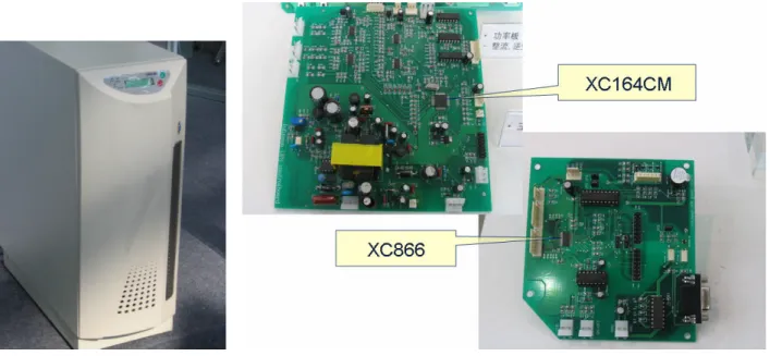
The 5KVA single-phase UPS reference design offers an integrated uninterrupted power supply solution with Infineon microcontrollers (Figure 1). Its main control process including PWM signals generation, output voltage feedback control, system faults and errors managing, charger module control, modules synchronization is all handled by the control board based on Infineon 16-bit microcontroller XC164CM. The information display with LCD and keyboard operations are implemented by the monitoring board based on Infineon 8-bit microcontrollers XC866 (Figure 1).
Figure 1 UPS System Block Diagram
The system block diagram of this UPS reference design is shown in Figure 2.
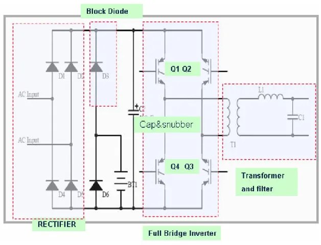
System Overview To eliminate the common noise, the input power is first filtered by an EMI filter which is connected to tow fuses. Afterwards the power flows into the passive power factor correction circuit in order to ensure the input current shape quality.
After reduction of voltage by an autotransformer, the input line voltage is rectified into DC voltage. The DC-bus voltage is then filtered and regulated by capacitors with a resistor in series which can restrain the inrush current. A relay is placed in parallel with the resistor and it will be closed to shorten this resistor when the DC-bus voltage reaches a certain value.
The battery module is connected with the DC-bus capacitors through a diode. If input line power blackout happens, the battery module will be switched to offer power to the inverter in order to keep the power uninterrupted.
The full-bridge inverter is utilized, whose output voltage is boosted by an isolating transformer and then filtered by the circuit consisting of inductor and capacitors. The leakage inductance of the transformer is adopted to filter out the high frequency and difference voltage. The output voltage of the inverter also provides power to the battery charger circuit. In “line” mode the charger circuit will receive the command to run from the control board, but in “bat” mode it always remains off.
A TRIAC is connected with the bypass relay via a switch. When overload or other fault occurs, the system will automatically switch to bypass mode so that the whole system as well as the load has got protection.
Figure 3 illustrates the topology utilized in this UPS reference design.
System Overview
2.2 Main Specifications
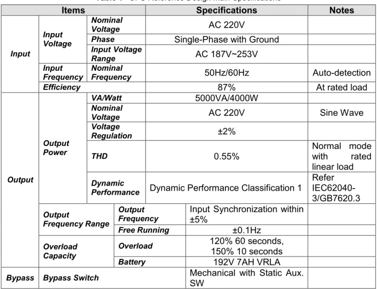
The main technical specifications of this UPS reference design are listed in Table 1.
Table 1 UPS Reference Design Main Specifications
Items Specifications Notes
Nominal
Voltage AC 220V
Phase Single-Phase with Ground
Input Voltage Input Voltage Range AC 187V~253V Input Frequency Nominal Frequency 50Hz/60Hz Auto-detection Input
Efficiency 87% At rated load
VA/Watt 5000VA/4000W
Nominal
Voltage AC 220V Sine Wave
Voltage Regulation ±2% THD 0.55% Normal mode with rated linear load Output Power Dynamic
Performance Dynamic Performance Classification 1
Refer IEC62040-3/GB7620.3
Output Frequency
Input Synchronization within ±5% Output Frequency Range Free Running ±0.1Hz Overload 120% 60 seconds, 150% 10 seconds Output Overload Capacity
Battery 192V 7AH VRLA
Bypass Bypass Switch Mechanical with Static Aux.
Main Control Principle
3
Main Control Principle
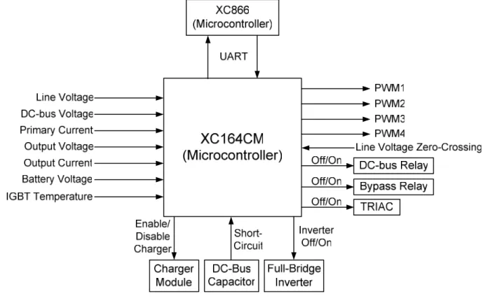
As introduced in the system overview section, an Infineon 16-bit microcontroller XC164CM is designed as the kernel of the main control circuit for the whole UPS system. The main control functions executed by the microcontroller are briefly illustrated in Figure 4.
Figure 4 Main Control Functions Overview
To obtain output which can be filtered into sine voltage, the full-bridge inverter should be driven by 4-channel signals with positive and negative cycles which can be originally generated by the microcontroller. These PWM signals from the microcontrollers are first isolated by optocouplers and then input to a flyback converter whose output can directly drive the inverter bridge.
Fault or error status associated with inverter is monitored and processed by the microcontroller. Once receiving fatal fault signals such as short circuit of the inverter or over temperature of IGBTs, the microcontroller will immediately close off all PWM output and generate disable signal to terminate the inverter operation. Therefore the protection function for inverter against severe damage is realized. After faults or errors have been released, all PWM signals will be resent out to run the inverter again for maintaining normal operation.
There are many physical parameters to be sampled by the Analog-Digital converter of the microcontroller and further calculated during main control process. These parameters include line voltage, DC-bus voltage, primary current of output transformer, output voltage, output current, battery voltage, IGBT temperature.
The charger module is enabled or disabled by the signal generated from the microcontroller depending on different states. In line mode it is launched into working so as to ensure full capacity of the battery voltage and is ceased to be inactive under the battery mode.
Main Control Principle The microcontroller is also in charge of the synchronization control of all modules of this UPS system as well as the inverter feedback control. The line voltage zero-crossing signal is captured by the microcontroller to synchronize the input voltage/phase with the output voltage/phase. The ON/OFF control signals for DC-bus relay and bypass relay along with TRIAC control signal are both produced by the microcontroller.
The display control board is designed based on an Infineon 8-bit microcontroller XC866 which needs to communicate with the microcontroller on the main control board for data transfer and receiving. Two necessary signals RxD and TxD are offered by the microcontroller to be connected with XC866 for implementing display of states, operation and errors information.
XC164CS Implementation of Main Control
4
XC164CS Implementation of Main Control
4.1 XC164CM Introduction
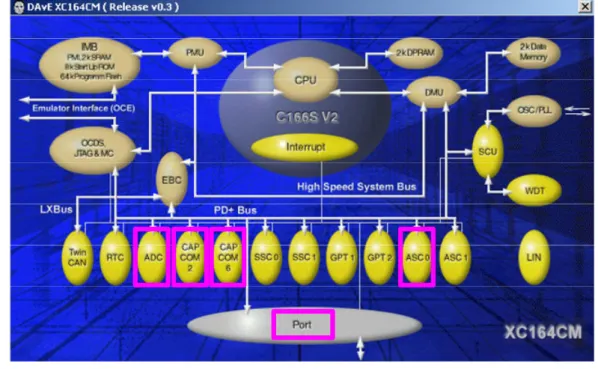
XC164CM is a member of the enhanced 16-bit microcontroller family XC166 which offers impressive DSP performance and advanced interrupt handling combined with a powerful integrated peripheral set and high performance, reliable on-chip Flash memory. The resource of Infineon 16-bit microcontroller XC164CM utilized in this UPS reference design is illustrated in Figure 5 (the modules encircled by magenta rectangles).
Figure 5 XC164CM Overview (DAvE Interface)
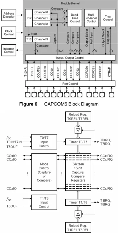
“CAPCOM6”: The CAPCOM6 unit is made up of a Timer T12 block with 3 capture/compare channels and a Timer T13 block with 1 compare channel. The T12 channels can independently generate PWM signals or accept capture triggers, or they can jointly generate control signal patterns to drive AC-motors or inverters. Its block diagram is shown on Figure 6.
“ADC”: Four conversion modes are supported: Fixed Channel Single Conversion mode, Fixed Channel Continuous Conversion mode, Auto Scan Single Conversion mode, Auto Scan Continuous Conversion mode. 8-bit or 10-bit resolution is alternative. DMA (PEC) support is available for result transfer to memory.
“CAPCOM2”: Two 16-bit timers (T7/T8) with reload registers provide 2 independent time bases for each capture/compare register array which contain 16 dual purpose capture/compare registers, each of which may be individually allocated to either timer T7 or T8 respectively and programmed for capture or compare operation. Figure 7 gives out its block diagram.
“Port”: Up to 47 general I/O pins are available in XC164CM. All port lines are individually bit-addressable and all I/O lines are independently programmable for input or output. The driver strength, open drain modes and input thresholds for dedicated ports are all programmable.
XC164CS Implementation of Main Control “ASC0”: It supports full-duplex asynchronous communication and half-duplex synchronous communication. The highlighted features include Loopback capability, autobaud detection unit for asynchronous operating modes, 8-stage FIFO with 9-Bit FIFO data width, etc.
Figure 6 CAPCOM6 Block Diagram
XC164CS Implementation of Main Control
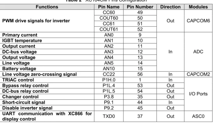
4.2 Pin Configuration
Table 2 indicates the configuration for all the XC164CM pins utilized in this UPS reference design.
Table 2 XC164CM Pins Configuration
Functions Pin Name Pin Number Direction Modules
CC60 49
COUT60 50
CC61 51
PWM drive signals for inverter
COUT61 52
Out CAPCOM6
Primary current AN0 9
IGBT temperature AN1 10
Output current AN2 11
DC-bus voltage AN3 12
Output voltage AN4 13
Line voltage AN5 14
Battery voltage AN10 15
In ADC
Line voltage zero-crossing signal CC22 56 In CAPCOM2
TRIAC control P1H.0 1 In
Bypass relay control P1L.4 53 Out
DC-bus relay control P1L.5 54 Out
Changer control P3.8 35 Out
Short-circuit signal P9.1 44 In
Disable inverter signal P9.2 45 Out
I/O Ports
UART communication with XC866 for
display control TXD0 37 Out ASC0
4.3 Initialization Settings
4.3.1 CAPCOM6
The CAPCOM6 initialization for PWM signal generation to drive the full-bridge inverter is summarized as follows (according to display order in DAvE):
“Module Clock”: Enable module.
“Pin Control”: Use pin CC60, CC61, COUT60, COUT61 as output. Pin CC62 is not used.
“T12”: fcpu/1 (Resolution: 0.025us), Center-aligned mode, T12 period 50us (carried frequency 20KHz), Enable interrupt for T12 period match (generating interrupt per carrier cycle), Dead-time 1.2us.
“T13”: No initialization is required for it isn’t used here. “Multi Ch.”: Disable multi-channel mode.
“Channels”: Compare and capture modes should be disabled for channel 2. Channel 0,1 should be individually configured as (x=0,1): Compare Mode 3 (Use pins CC6x/COUT6x as output); Enable T12 modulation for CC6x; The compare output CC6x drives passive level while CC6xST is “1”; The compare output COUT6x drives passive level while CC6xST is “0”; The passive level of CC6x and COUT6x output are all “0”; Enable dead time generation.
XC164CS Implementation of Main Control “Trap/INT”: Do not use pin #CTRAP as input. In “Interrupt Configuration” Enable T12
interrupt/node I2.
“Interrupts”: CCU6 I2 INT -> Level 14, Group 2.
“Functions”: In “Initialization Function” select “CCU6_vInit”; In “Function Library (Part 1)” select “CCU6_vStartTmr”, “CCU6_vStopTmr”, “CCU6_vResetTmr”, “CCU6_vEnableShadowTransfer”.
4.3.2 ADC
The ADC initialization for sampling physical parameters is summarized as (according to display order in DAvE):
“Module Clock”: Enable module.
“Control”: Select “Enhanced Mode”. In “Enhanced Mode” select “Fixed channel single conversion”; 10-bit resolution; In “Analog Channel Input Selection” select “Analog channel 2”; Conversion basic clock is fcpu/1 (tbc=25ns); Sample time is tbc*8=200ns.
“Port Control”: Disconnect all digital input stages from port P5.
“Functions”: In “Initialization Function” select “ADC_vInit”; In “Function Library (Part 1)” select “ADC_vStartConv”, “ADC_uwReadConv”.
4.3.3 CAPCOM2
The CAPCOM2 initialization for capturing line voltage zero-crossing signal is summarized as (according to display order in DAvE):
“Module Clock”: Enable module.
“Control”: The content of the port register is changed by the CAPCOM2 unit. “Timer7/8”: Timer 7 Input Selection as “Module Clock / 32 (Resolution: 0.8us)” “Channels”: In “Configure channel 22” select “Capture on positive transition at pin
CC22IO (P1L.7)”; CC22 allocated to timer T7; Enable Capture/Compare interrupt (IE).
“Interrupts”: CC2 ch22 INT -> Level 14, Group 0.
“Functions”: In “Initialization Function” select “CC2_vInit”; In “Function Library (Part 1)” Select “CC2_vStartTmr”, “CC2_vStopTmr”, “CC2_vClearTmr”.
4.3.4 I/O Ports
The “Port” module in DAvE is configured as:
P1H.0 as general IO, In; P1L.4/P1L.5 as general IO, Out; P3.8 as general IO, Out, Open drain;
XC164CS Implementation of Main Control
4.3.5 ASC0
The ASC0 initialization for communicating with XC866 on the display board is summarized as below (according to display order in DAvE):
“Module Clock”: Enable module.
“Pin Selection”: Full-duplex asynchronous operating modes; Use pin TxDA0 (P3.10); Use pin RxDA0 (P3.11).
“Control ”: 8-bit data (asynchronous); One stop bit; Enable receiver (REN). “Baud Rate”: Additionally reduce serial clock to 2; Enable baud rate generator;
Required baud rate 9.6k.
“Functions”: In “Initialization Function” select “ASC0_vInit”. 4.4 Some Programming Considerations
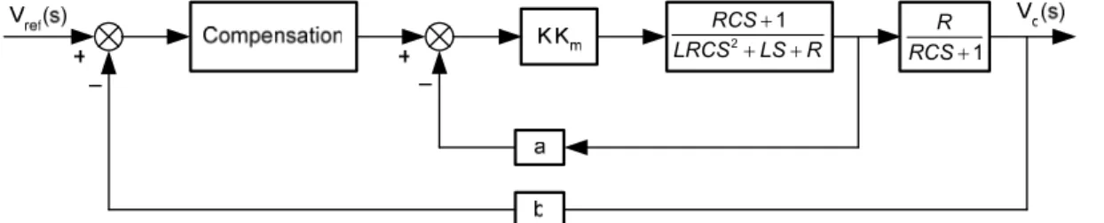
In CCU6 T12 period-match interrupt service routine, the output current and voltage, primary current, line voltage, battery voltage and IGBT temperature are all sampled. Here the dual-loop control strategy is utilized so the primary current and output voltage are both involved to control the inverter. Figure 8 shows the block diagram of this control scheme.
R LS LRCS RCS + + + 2 1 1 + RCS R
Figure 8 Dual-loop Control Block Diagram
It can be calculated that the proportion coefficient ki of the current loop is 1.4. The equation for compensation link of the voltage loop can be described as
1 003 . 0 30 8 . 2 ) ( + + = s s yCL (E-1) The difference equation can be derived that
y(k)=3.0848 ⋅e(k)−2.506⋅e(k −1)+0.9835⋅y(k −1) (E-2) where y(k) is the output value of the compensation and e(k) is the error value.
The width of the SPWM signal which drives the inverter can be calculated by + × = 0.5 softstart 1 cm g K U U PW (E-3) where Ksoftstart is the modulation coefficient. To avoid inrush current at start-up, soft starting operation is required. The value of m is increased to get better performance for soft starting.
The RMS value of the output voltage is also calculated to modify the reference sine table to meet the voltage regulation specification. The maximum amplitude of the output
XC164CS Implementation of Main Control voltage 220× 2 ≈311 (volts) can be normalized with a number 30967. So after being attenuated by sampling circuit and knocked off by the DC offset, the AD convertion result of the output voltage should be multiplied by 16.004 for normalization. The output value of the voltage loop is also normalized to be limited between 48000 and –48000. Suppose that the maximum positive value of the primary current is 130A and the attenuation coefficient is 22/2000 =0.011, then the original AD conversion result is 130×0.011×4096/5 =1171. Therefore all the AD conversion results of the primary current should be multiplied by
41 1171 /
48000 = for normalization in order to be limited within the output range of voltage
loop.
The value of the 90° point of modulated sine wave is also detected in the T12 period-match interrupt service routine. If short-circuit fault occurs on the output of the inverter, the value of this point will be lower than the set value 400, which represents 68 volts of the output voltage.
The zero-crossing point of the line voltage is calculated and detected to trigger the CAPCOM2 external interrupt. In order to save operation time, the average value of the line voltage is calculated instead of RMS. The relationship between the average value and the RMS value is (for 50Hz): 1.11 ) 50 2 sin( 311 02 . 0 220 02 . 0 0 = ⋅ × ×
∫
t dt Urms π (E-4)In this interrupt service routine, when lock signal is available, If the measured phase of reference is less than180°, the pointer for the reference sine table will be increased with 1 point. If it is larger than180°, this pointer will be decreased with 1 point.
XC164CS Implementation of Main Control
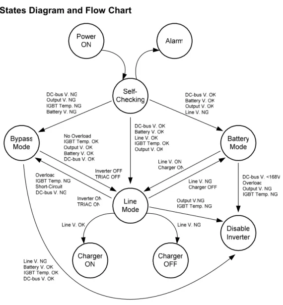
4.5 States Diagram and Flow Chart
Figure 9 States Diagram for Main Control
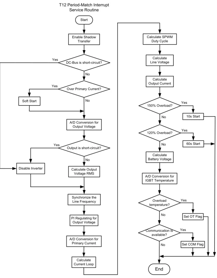
Figure 9 illustrates the state diagram for main control. The flowchart for T12 period-match interrupt service routine is shown in Figure 10.
XC164CS Implementation of Main Control Start T12 Period-Match Interrupt Service Routine Enable Shadow Transfer DC-Bus is short-circuit?
Over Primary Current? No
No
A/D Conversion for Output Voltage Output is short-circuit? No Calculate Output Voltage RMS Synchronize the Line Frequency PI Regulating for Output Voltage
A/D Conversion for Primary Current Yes Soft Start Yes Disable Inverter Yes Calculate Current Loop Calculate SPWM Duty Cycle Calculate Line Voltage Calculate Output Current 150% Overload? 120% Overload? Calculate Battery Voltage No No
A/D Conversion for IGBT Temperature Overload temperature? Communication is available? End No No Yes Yes Set OT Flag
Set COM Flag Yes
Yes 10s Start
60s Start
Experiment Results
5
Experiment Results
Figure 11 shows the measured filtered output voltage waveforms with feedback under no-load and rated resistant load conditions respectively.
(a) Without Load (b) With Rated Resistant Load
Figure 11 Measured Output Voltage Waveforms
Figure 12(a) records the output transient response waveform with full resistant load taken ON under line mode without connecting any battery. The waveform for dynamic performance under battery mode is shown in Figure 12(b).
(a) Line Mode (No Battery) (b) Battery Mode
Figure 12 Output Transient Response
Figure 13 illustrates the short-circuit protection action, where channel 1 is for output current and channel 4 is for output voltage.
The phase difference between the output voltage and the line voltage is shown in Figure 14, where channel 1 is for the output and channel 4 is for the line power. The time interval between two zero-crossing points is 95us.
Figure 15 displays the bypass relay and TRIAC actions under overload condition, in which channel A is for output voltage and channel C is for bypass current.
Experiment Results
Figure 13 Short-Circuit Protection
Figure 14 Synchronization
Conclusions
6
Conclusions
The main control part of UPS (Uninterrupted Power Supply) system is traditionally designed with analog components. Due to the complicated circuit structure and difficulty in debugging, the current trend for UPS design is to adopt a microcontroller as a main control center instead of the analog solution.
This application note intends to provide an introduction of XC164CM main control implementation for a 5KVA single-phase UPS reference design. Owe to the high performance of XC164CM, the excellent digital closed-loop characteristic of this UPS system has been obtained.
http://www. inf ineo n.c om