1. General
description
The LPC11E6x are an ARM Cortex-M0+ based, low-cost 32-bit MCU family operating at CPU frequencies of up to 50 MHz. The LPC11E6x support up to 256 KB of flash memory, a 4 KB EEPROM, and 36 KB of SRAM.
The ARM Cortex-M0+ is an easy-to-use, energy-efficient core using a two-stage pipeline and fast single-cycle I/O access.
The peripheral complement of the LPC11E6x includes a DMA controller, a CRC engine, two I2C-bus interfaces, up to five USARTs, two SSP interfaces, PWM/timer subsystem
with six configurable multi-purpose timers, a Real-Time Clock, one 12-bit ADC, temperature sensor, function-configurable I/O ports, and up to 80 general-purpose I/O pins.
For additional documentation related to the LPC11E6x parts, see Section 18 “References”.
2. Features and benefits
System:
ARM Cortex-M0+ processor (version r0p1), running at frequencies of up to 50 MHz with single-cycle multiplier and fast single-cycle I/O port.
ARM Cortex-M0+ built-in Nested Vectored Interrupt Controller (NVIC). AHB Multilayer matrix.
System tick timer.
Serial Wire Debug (SWD) and JTAG boundary scan modes supported. Micro Trace Buffer (MTB) supported.
Memory:
Up to 256 KB on-chip flash programming memory with page erase. Up to 32 KB main SRAM.
Up to two additional SRAM blocks of 2 KB each.
Up to 4 KB EEPROM.
ROM API support: Boot loader. USART drivers. I2C drivers. DMA drivers. Power profiles.
Flash In-Application Programming (IAP) and In-System Programming (ISP).
and 36 kB SRAM; 4 kB EEPROM; 12-bit ADC
32-bit integer division routines. Digital peripherals:
Simple DMA engine with 16 channels and programmable input triggers.
High-speed GPIO interface connected to the ARM Cortex-M0+ IO bus with up to 80 General-Purpose I/O (GPIO) pins with configurable pull-up/pull-down resistors, programmable open-drain mode, input inverter, and programmable glitch filter and digital filter.
Pin interrupt and pattern match engine using eight selectable GPIO pins. Two GPIO group interrupt generators.
CRC engine.
Configurable PWM/timer subsystem (two 16-bit and two 32-bit standard counter/timers, two State-Configurable Timers (SCTimer/PWM)) that provides:
Up to four 32-bit and two 16-bit counter/timers or two 32-bit and six 16-bit counter/timers.
Up to 21 match outputs and 16 capture inputs.
Up to 19 PWM outputs with 6 independent time bases. Windowed WatchDog timer (WWDT).
Real-time Clock (RTC) in the always-on power domain with separate battery supply pin and 32 kHz oscillator.
Analog peripherals:
One 12-bit ADC with up to 12 input channels with multiple internal and external trigger inputs and with sample rates of up to 2 Msamples/s. The ADC supports two independent conversion sequences.
Temperature sensor. Serial interfaces:
Up to five USART interfaces, all with DMA, synchronous mode, and RS-485 mode support. Four USARTs use a shared fractional baud generator.
Two SSP controllers with DMA support.
Two I2C-bus interfaces. One I2C-bus interface with specialized open-drain pins
supports I2C Fast-mode Plus. Clock generation:
12 MHz internal RC oscillator trimmed to 1 % accuracy for 25C Tamb +85C
that can optionally be used as a system clock. On-chip 32 kHz oscillator for RTC.
Crystal oscillator with an operating range of 1 MHz to 25 MHz. Oscillator pins are shared with the GPIO pins.
Programmable watchdog oscillator with a frequency range of 9.4 kHz to 2.3 MHz. PLL allows CPU operation up to the maximum CPU rate without the need for a
high-frequency crystal.
Clock output function with divider that can reflect the crystal oscillator, the main clock, the IRC, or the watchdog oscillator.
Power control:
Integrated PMU (Power Management Unit) to minimize power consumption. Reduced power modes: Sleep mode, Deep-sleep mode, Power-down mode, and
Deep power-down mode.
Power-On Reset (POR). Brownout detect.
Unique device serial number for identification. Single power supply (2.4 V to 3.6 V).
Separate VBAT supply for RTC.
Operating temperature range -40 °C to 105 °C.
Available as LQFP48, LQFP64, and LQFP100 packages.
3. Applications
4. Ordering
information
4.1 Ordering options
Three-phase e-meter Car radio
GPS tracker Medical monitor
Gaming accessories PC peripherals
Table 1. Ordering information
Type number Package
Name Description Version
LPC11E66JBD48 LQFP48 plastic low profile quad flat package; 48 leads; body 7 7 1.4 mm SOT313-2
LPC11E67JBD48 LQFP48 plastic low profile quad flat package; 48 leads; body 7 7 1.4 mm SOT313-2
LPC11E67JBD64 LQFP64 plastic low profile quad flat package; 64 leads; body 10 10 1.4 mm SOT314-2
LPC11E67JBD100 LQFP100 plastic low profile quad flat package; 100 leads; body 14 14 1.4 mm SOT407-1
LPC11E68JBD48 LQFP48 plastic low profile quad flat package; 48 leads; body 7 7 1.4 mm SOT313-2
LPC11E68JBD64 LQFP64 plastic low profile quad flat package; 64 leads; body 10 10 1.4 mm SOT314-2
LPC11E68JBD100 LQFP100 plastic low profile quad flat package; 100 leads; body 14 14 1.4 mm SOT407-1
Table 2. Ordering options
Type number Flash/ KB
EEPROM/ KB
SRAM/ KB
USART0 USART1 USART2 USART3 USART4
I2C SSP PWM/ timers 12-bit ADC channels GPIO LPC11E66JBD48 64 4 12 Y Y Y Y N 2 2 6 8 36 LPC11E67JBD48 128 4 20 Y Y Y Y N 2 2 6 8 36 LPC11E67JBD64 128 4 20 Y Y Y Y N 2 2 6 10 50 LPC11E67JBD100 128 4 20 Y Y Y Y Y 2 2 6 12 80 LPC11E68JBD48 256 4 36 Y Y Y Y N 2 2 6 8 36 LPC11E68JBD64 256 4 36 Y Y Y Y N 2 2 6 10 50 LPC11E68JBD100 256 4 36 Y Y Y Y Y 2 2 6 12 80
5. Marking
5.1 Product identification
The LPC11E6x devices typically have the following top-side marking for LQFP100 packages:
LPC11E6xJBD100 xxxxxx xx
xxxyywwxR[x]
The LPC11E6x devices typically have the following top-side marking for LQFP64 packages:
LPC11E6xJ xxxxxx xx xxxyywwxR[x]
The LPC11E6x devices typically have the following top-side marking for LQFP48 packages:
LPC11E6xJ xx xx xxxyy wwxR[x]
Field ‘yy’ states the year the device was manufactured. Field ‘ww’ states the week the device was manufactured during that year.
Field ‘R’ identifies the device revision.
Fig 1. LQFP64/100 package marking Fig 2. LQFP48 package marking
1 n Terminal 1 index area
aaa-011231 Terminal 1 index area aaa-011232 1
6. Block
diagram
Gray-shaded blocks show peripherals that can provide hardware triggers for DMA transfers or have DMA request lines. (1) Available on LQFP100 packages only.
Fig 3. LPC11E6x block diagram
ARM CORTEX-M0+ SWD TEST/DEBUG INTERFACE SYSTICK NVIC PROCESSOR CORE PRECISION IRC SYSTEM PLL WATCHDOG OSCILLATOR SYSTEM OSCILLATOR RTC OSCILLATOR GENERAL PURPOSE BACKUP REGISTERS CLOCK GENERATION 256/128/64 KB FLASH ROM 36/20/12 KB SRAM 4 KB EEPROM TEMPERATURE SENSOR MEMORY PORT0/1/2 GINT0/1 PINTSEL PINT/ PATTERN MATCH SCTIMER0/ PWM HS GPIO+ SCTIMER1/ PWM DMA TRIGGER PWM/TIMER SUBSYSTEM USART0 USART1 USART3 USART4(1) FM+ I2C0 USART2 SSP1 SSP0 I2C1
SYSCON IOCON PMU CRC FLASH CTRL EEPROM CTRL
SYSTEM/MEMORY CONTROL
CT16B0 CT32B0
CT16B1 CT32B1
WWDT RTC
ALWAYS-ON POWER DOMAIN SYSTEM TIMER
SERIAL PERIPHERALS 12-bit ADC0 TRIGGER MUX ANALOG PERIPHERALS AHB MULTILAYER MATRIX AHB/APB BRIDGES DMA LPC11E6x pads n IOCON aaa-011045
7. Pinning
information
7.1 Pinning
Fig 4. LQFP48 pinning LPC11E6XJBD48 37 SWDIO/PIO0_15 24 PIO0_7 38 PIO0_16/WAKEUP 23 PIO0_6 39 PIO0_23 22 PIO1_24 40 VDDA 21 PIO2_4 41 VSSA 20 PIO2_7 42 PIO0_17 19 PIO2_3 43 VSS 18 PIO1_23 44 VDD 17 PIO0_21 45 PIO0_18 16 PIO0_5 46 PIO0_19 15 PIO0_4 47 VBAT 14 PIO0_3 48 RTCXIN 13 PIO1_20 1 RT C X O U T 36 PIO1_13 2 VSS 35 VREFN 3 RESET/PIO0_0 34 VREFP 4 PIO0_1 33 TRST/PIO0_14 5 VSS 32 TDO/PIO0_13 6 PIO2_0/XT ALIN 31 TMS/PIO0_12 7 PIO2_1/XT ALOUT 30 TDI/PIO0_1 1 8 VDD 29 PIO0_22 9 PIO2_5 28 SWCLK/PIO0_10 10 PIO0_20 27 PIO0_9 11 PIO0_2 26 PIO0_8 12 PIO2_2 25 PIO1_21 aaa-011046Fig 5. LQFP64 pinning LPC11E6XJBD64 49 PIO1_13 32 PIO2_15 50 SWDIO/PIIO0_15 31 PIO1_28 51 PIO0_16/WAKEUP 30 PIO0_7 52 PIO0_23 29 PIO0_6 53 VDDA 28 PIO1_24 54 VSSA 27 PIO2_4 55 PIO1_9 26 PIO2_7 56 PIO0_17 25 PIO2_6 57 VSS 24 PIO2_3 58 VDD 23 PIO1_23 59 VDD 22 PIO0_21 60 PIO0_18 21 PIO0_5 61 PIO0_19 20 PIO0_4 62 PIO1_0 19 PIO0_3 63 VBAT 18 PIO1_20 64 PIO1_19 17 PIO1_27 1 RT C X IN 48 VREFN 2 RT C X O U T 47 VREFP 3 VSS 46 TRST/PIO0_14 4 RESET/PIO0_0 45 TDO/PIO0_13 5 PIO0_1 44 PIO1_30 6 PIO1_7 43 TMS/PIO0_12 7 VSS 42 TDI/PIO0_1 1 8 PIO2_0 41 PIO1_29 9 PIO2_1 40 PIO0_22 10 VDD 39 SWCLK/PIO0_10 11 PIO2_5 38 PIO0_9 12 PIO0_20 37 PIO0_8 13 PIO1_10 36 PIO2_19 14 PIO0_2 35 PIO1_21 15 PIO1_26 34 VDD 16 PIO2_2 33 PIO2_18 aaa-011047 Fig 6. LQFP100 pinning LPC11E6XJBD100 76 100 50 26 1 25 75 51 aaa-011048
7.2 Pin description
Table 3. Pin description
Pin functions are selected through the IOCON registers. See Table 2 for availability of USART4 pin functions.
Symbol LQ FP 48 LQ FP 64 LQ FP 10 0 Reset state[1]
Type Description of pin functions
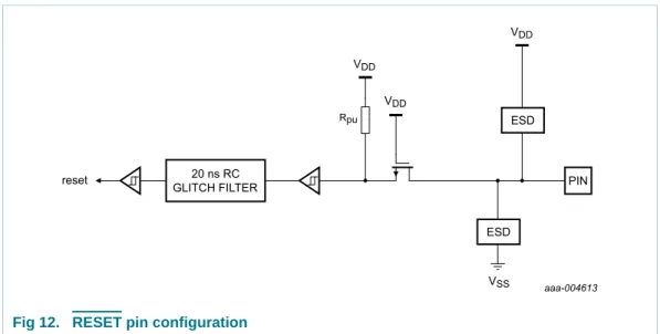
RESET/PIO0_0
3 4 8 [8] I; PU I RESET — External reset input with 20 ns glitch filter. A
LOW-going pulse as short as 50 ns on this pin resets the device, causing I/O ports and peripherals to take on their default states, and processor execution to begin at address 0. This pin also serves as the debug select input. LOW level selects the JTAG boundary scan. HIGH level selects the ARM SWD debug mode.
In deep power-down mode, this pin must be pulled HIGH externally. The RESET pin can be left unconnected or be used as a GPIO pin if an external RESET function is not needed and Deep power-down is not used.
IO PIO0_0 — General-purpose digital input/output pin. PIO0_1
4 5 9 [6] I; PU IO PIO0_1 — General-purpose digital input/output pin. A
LOW level on this pin during reset starts the ISP command handler.
O CLKOUT — Clockout pin.
O CT32B0_MAT2 — Match output 2 for 32-bit timer 0. PIO0_2
11 14 19 [6] I; PU IO PIO0_2 — General-purpose port 0 input/output 2.
IO SSP0_SSEL — Slave select for SSP0.
I CT16B0_CAP0 — Capture input 0 for 16-bit timer 0. - R_0 — Reserved.
PIO0_3
14 19 30 [6] I; PU IO PIO0_3 — General-purpose digital input/output pin.
- R — Reserved.
R_1 — Reserved. PIO0_4
15 20 31 [7] IA IO PIO0_4 — General-purpose port 0 input/output 4
(open-drain).
IO I2C0_SCL — I2C-bus clock input/output (open-drain). High-current sink only if I2C Fast-mode Plus is selected in the I/O configuration register.
- R_2 — Reserved. PIO0_5
16 21 32 [7] IA IO PIO0_5 — General-purpose port 0 input/output 5
(open-drain).
IO I2C0_SDA — I2C-bus data input/output (open-drain). High-current sink only if I2C Fast-mode Plus is selected in the I/O configuration register.
- R_3 — Reserved. PIO0_6
23 29 44 [6] I; PU IO PIO0_6 — General-purpose port 0 input/output 6.
- R — Reserved.
IO SSP0_SCK — Serial clock for SSP0. - R_4 — Reserved.
PIO0_7
24 30 45 [5] I; PU IO PIO0_7 — General-purpose port 0 input/output 7
(high-current output driver).
I U0_CTS — Clear To Send input for USART. - R_5 — Reserved.
IO I2C1_SCL — I2C-bus clock input/output. This pin is not open-drain.
PIO0_8
26 37 58 [6] I; PU IO PIO0_8 — General-purpose port 0 input/output 8.
IO SSP0_MISO — Master In Slave Out for SSP0. O CT16B0_MAT0 — Match output 0 for 16-bit timer 0. - R_6 — Reserved.
PIO0_9
27 38 59 [6] I; PU IO PIO0_9 — General-purpose port 0 input/output 9.
IO SSP0_MOSI — Master Out Slave In for SSP0. O CT16B0_MAT1 — Match output 1 for 16-bit timer 0. - R_7 — Reserved.
SWCLK/PIO0_10
28 39 60 [6] I; PU IO SWCLK — Serial Wire Clock. SWCLK is enabled by
default on this pin. In boundary scan mode: TCK (Test Clock).
IO PIO0_10 — General-purpose digital input/output pin. IO SSP0_SCK — Serial clock for SSP0.
O CT16B0_MAT2 — 16-bit timer0 MAT2 TDI/PIO0_11
30 42 64 [3] I; PU IO TDI — Test Data In for JTAG interface. In boundary scan
mode only.
IO PIO0_11 — General-purpose digital input/output pin. AI ADC_9 — A/D converter, input channel 9.
O CT32B0_MAT3 — Match output 3 for 32-bit timer 0. O U1_RTS — Request To Send output for USART1. IO U1_SCLK — Serial clock input/output for USART1 in
synchronous mode. TMS/PIO0_12
31 43 66 [3] I; PU IO TMS — Test Mode Select for JTAG interface. In boundary
scan mode only.
IO PIO0_12 — General-purpose digital input/output pin. AI ADC_8 — A/D converter, input channel 8.
I CT32B1_CAP0 — Capture input 0 for 32-bit timer 1. I U1_CTS — Clear To Send input for USART1. TDO/PIO0_13
32 45 68 [3] I; PU IO TDO — Test Data Out for JTAG interface. In boundary
scan mode only.
IO PIO0_13 — General-purpose digital input/output pin. AI ADC_7 — A/D converter, input channel 7.
O CT32B1_MAT0 — Match output 0 for 32-bit timer 1. I U1_RXD — Receiver input for USART1.
Table 3. Pin description
Pin functions are selected through the IOCON registers. See Table 2 for availability of USART4 pin functions.
Symbol LQ FP4 8 LQ FP6 4 LQ FP1 0 0 Reset state[1]
TRST/PIO0_14
33 46 69 [3] I; PU IO TRST — Test Reset for JTAG interface. In boundary scan
mode only.
IO PIO0_14 — General-purpose digital input/output pin. AI ADC_6 — A/D converter, input channel 6.
O CT32B1_MAT1 — Match output 1 for 32-bit timer 1. O U1_TXD — Transmitter output for USART1. SWDIO/PIO0_15
37 50 81 [3] I; PU IO SWDIO — Serial Wire Debug I/O. SWDIO is enabled by
default on this pin. In boundary scan mode: TMS (Test Mode Select).
IO PIO0_15 — General-purpose digital input/output pin. AI ADC_3 — A/D converter, input channel 3.
O CT32B1_MAT2 — Match output 2 for 32-bit timer 1. PIO0_16/WAKEUP
38 51 82 [4] I; PU IO PIO0_16 — General-purpose digital input/output pin. This
pin also serves as the Deep power-down mode wake-up pin with 20 ns glitch filter. Pull this pin HIGH externally before entering Deep power-down mode. Pull this pin LOW to exit Deep power-down mode. A LOW-going pulse as short as 50 ns wakes up the part.
I ADC_2 — A/D converter, input channel 2.
O CT32B1_MAT3 — Match output 3 for 32-bit timer 1. - R_8 — Reserved.
PIO0_17
42 56 90 [6] I; PU IO PIO0_17 — General-purpose digital input/output pin.
O U0_RTS — Request To Send output for USART0. I CT32B0_CAP0 — Capture input 0 for 32-bit timer 0. IO U0_SCLK — Serial clock input/output for USART0 in
synchronous mode. PIO0_18
45 60 94 [6] I; PU IO PIO0_18 — General-purpose digital input/output pin.
I U0_RXD — Receiver input for USART0. Used in UART ISP mode.
O CT32B0_MAT0 — Match output 0 for 32-bit timer 0. PIO0_19
46 61 95 [6] I; PU IO PIO0_19 — General-purpose digital input/output pin.
O U0_TXD — Transmitter output for USART0. Used in UART ISP mode.
O CT32B0_MAT1 — Match output 1 for 32-bit timer 0. PIO0_20
10 12 17 [6] I; PU IO PIO0_20 — General-purpose digital input/output pin.
I CT16B1_CAP0 — Capture input 0 for 16-bit timer 1. I U2_RXD — Receiver input for USART2.
PIO0_21
17 22 33 [6] I; PU IO PIO0_21 — General-purpose digital input/output pin.
O CT16B1_MAT0 — Match output 0 for 16-bit timer 1. IO SSP1_MOSI — Master Out Slave In for SSP1.
Table 3. Pin description
Pin functions are selected through the IOCON registers. See Table 2 for availability of USART4 pin functions.
Symbol LQ FP4 8 LQ FP6 4 LQ FP1 0 0 Reset state[1]
PIO0_22
29 40 62 [3] I; PU IO PIO0_22 — General-purpose digital input/output pin.
AI ADC_11 — A/D converter, input channel 11. I CT16B1_CAP1 — Capture input 1 for 16-bit timer 1. IO SSP1_MISO — Master In Slave Out for SSP1. PIO0_23
39 52 83 [3] I; PU IO PIO0_23 — General-purpose digital input/output pin.
AI ADC_1 — A/D converter, input channel 1. - R_9 — Reserved.
I U0_RI — Ring Indicator input for USART0. IO SSP1_SSEL — Slave select for SSP1. PIO1_0
- 62 97 [6] I; PU IO PIO1_0 — General-purpose digital input/output pin.
O CT32B1_MAT0 — Match output 0 for 32-bit timer 1. - R_10 — Reserved.
O U2_TXD — Transmitter output for USART2. PIO1_1
- - 28 [6] I; PU IO PIO1_1 — General-purpose digital input/output pin.
O CT32B1_MAT1 — Match output 1 for 32-bit timer 1. - R_11 — Reserved.
O U0_DTR — Data Terminal Ready output for USART0. PIO1_2
- - 55 [6] I; PU IO PIO1_2 — General-purpose digital input/output pin.
O CT32B1_MAT2 — Match output 2 for 32-bit timer 1. - R_12 — Reserved.
I U1_RXD — Receiver input for USART1. PIO1_3
- - 72 [3] I; PU IO PIO1_3 — General-purpose digital input/output pin.
O CT32B1_MAT3 — Match output 3 for 32-bit timer 1. - R_13 — Reserved.
IO I2C1_SDA — I2C-bus data input/output (not open-drain). AI ADC_5 — A/D converter, input channel 5.
PIO1_4
- - 23 [6] I; PU IO PIO1_4 — General-purpose digital input/output pin.
I CT32B1_CAP0 — Capture input 0 for 32-bit timer 1. - R_14 — Reserved.
I U0_DSR — Data Set Ready input for USART0. PIO1_5
- - 47 [6] I; PU IO PIO1_5 — General-purpose digital input/output pin.
I CT32B1_CAP1 — Capture input 1 for 32-bit timer 1. - R_15 — Reserved.
I U0_DCD — Data Carrier Detect input for USART0. PIO1_6
- - 98 [6] I; PU IO PIO1_6 — General-purpose digital input/output pin.
- R_16 — Reserved.
I U2_RXD — Receiver input for USART2.
I CT32B0_CAP1 — Capture input 1 for 32-bit timer 0.
Table 3. Pin description
Pin functions are selected through the IOCON registers. See Table 2 for availability of USART4 pin functions.
Symbol LQ FP4 8 LQ FP6 4 LQ FP1 0 0 Reset state[1]
PIO1_7
- 6 10 [6] I; PU IO PIO1_7 — General-purpose digital input/output pin.
- R_17 — Reserved.
I U2_CTS — Clear To Send input for USART2. I CT16B1_CAP0 — Capture input 0 for 32-bit timer 1. PIO1_8
- - 61 [6] I; PU IO PIO1_8 — General-purpose digital input/output pin.
- R_18 — Reserved.
O U1_TXD — Transmitter output for USART1.
I CT16B0_CAP0 — Capture input 0 for 16-bit timer 0. PIO1_9
- 55 86 [3] I; PU IO PIO1_9 — General-purpose digital input/output pin.
I U0_CTS — Clear To Send input for USART0. O CT16B1_MAT1 — Match output 1 for 16-bit timer 1. AI ADC_0 — A/D converter, input channel 0.
PIO1_10
- 13 18 [6] I; PU IO PIO1_10 — General-purpose digital input/output pin.
O U2_RTS — Request To Send output for USART2. IO U2_SCLK — Serial clock input/output for USART2 in
synchronous mode.
O CT16B1_MAT0 — Match output 0 for 16-bit timer 1. PIO1_11
- - 65 [6] I; PU IO PIO1_11 — General-purpose digital input/output pin.
IO I2C1_SCL — I2C1-bus clock input/output (not open-drain). O CT16B0_MAT2 — Match output 2 for 16-bit timer 0. I U0_RI — Ring Indicator input for USART0.
PIO1_12
- - 89 [6] I; PU IO PIO1_12 — General-purpose digital input/output pin.
IO SSP0_MOSI — Master Out Slave In for SSP0. O CT16B0_MAT1 — Match output 1 for 16-bit timer 0. - R_21 — Reserved.
PIO1_13
36 49 78 [6] I; PU IO PIO1_13 — General-purpose digital input/output pin.
I U1_CTS — Clear To Send input for USART1. O SCT0_OUT3 — SCTimer0/PWM output 3. - R_22 — Reserved.
PIO1_14
- - 79 [6] I; PU IO PIO1_14 — General-purpose digital input/output pin.
IO I2C1_SDA — I2C1-bus data input/output (not open-drain). O CT32B1_MAT2 — Match output 2 for 32-bit timer 1. - R_23 — Reserved.
PIO1_15
- - 87 [6] I; PU IO PIO1_15 — General-purpose digital input/output pin.
IO SSP0_SSEL — Slave select for SSP0.
O CT32B1_MAT3 — Match output 3 for 32-bit timer 1. - R_24 — Reserved.
Table 3. Pin description
Pin functions are selected through the IOCON registers. See Table 2 for availability of USART4 pin functions.
Symbol LQ FP4 8 LQ FP6 4 LQ FP1 0 0 Reset state[1]
PIO1_16
- - 96 [6] I; PU IO PIO1_16 — General-purpose digital input/output pin.
IO SSP0_MISO — Master In Slave Out for SSP0. O CT16B0_MAT0 — Match output 0 for 16-bit timer 0. - R_25 — Reserved.
PIO1_17
- - 34 [6] I; PU IO PIO1_17 — General-purpose digital input/output pin.
I CT16B0_CAP2 — Capture input 2 for 16-bit timer 0. I U0_RXD — Receiver input for USART0.
- R_26 — Reserved. PIO1_18
- - 43 [6] I; PU IO PIO1_18 — General-purpose digital input/output pin.
I CT16B1_CAP1 — Capture input 1 for 16-bit timer 1. O U0_TXD — Transmitter output for USART0.
- R_27 — Reserved. PIO1_19
- 64 4 [6] I; PU IO PIO1_19 — General-purpose digital input/output pin.
I U2_CTS — Clear To Send input for USART2. O SCT0_OUT0 — SCTimer0/PWM output 0. - R_28 — Reserved.
PIO1_20
13 18 29 [6] I; PU IO PIO1_20 — General-purpose digital input/output pin.
I U0_DSR — Data Set Ready input for USART0. IO SSP1_SCK — Serial clock for SSP1.
O CT16B0_MAT0 — Match output 0 for 16-bit timer 0. PIO1_21
25 35 56 [6] I; PU IO PIO1_21 — General-purpose digital input/output pin.
I U0_DCD — Data Carrier Detect input for USART0. IO SSP1_MISO — Master In Slave Out for SSP1. I CT16B0_CAP1 — Capture input 1 for 16-bit timer 0. PIO1_22
- - 80 [3] I; PU IO PIO1_22 — General-purpose digital input/output pin.
IO SSP1_MOSI — Master Out Slave In for SSP1. I CT32B1_CAP1 — Capture input 1 for 32-bit timer 1. AI ADC_4 — A/D converter, input channel 4.
- R_29 — Reserved. PIO1_23
18 23 35 [6] I; PU IO PIO1_23 — General-purpose digital input/output pin.
O CT16B1_MAT1 — Match output 1 for 16-bit timer 1. IO SSP1_SSEL — Slave select for SSP1.
O U2_TXD — Transmitter output for USART2. PIO1_24
22 28 42 [6] I; PU IO PIO1_24 — General-purpose digital input/output pin.
O CT32B0_MAT0 — Match output 0 for 32-bit timer 0. IO I2C1_SDA — I2C-bus data input/output (not open-drain).
Table 3. Pin description
Pin functions are selected through the IOCON registers. See Table 2 for availability of USART4 pin functions.
Symbol LQ FP4 8 LQ FP6 4 LQ FP1 0 0 Reset state[1]
PIO1_25
- - 100 [6] I; PU IO PIO1_25 — General-purpose digital input/output pin.
O U2_RTS — Request To Send output for USART2. IO U2_SCLK — Serial clock input/output for USART2 in
synchronous mode.
I SCT0_IN0 — SCTimer0/PWM input 0. - R_30 — Reserved.
PIO1_26
- 15 20 [6] I; PU IO PIO1_26 — General-purpose digital input/output pin.
O CT32B0_MAT2 — Match output 2 for 32-bit timer 0. I U0_RXD — Receiver input for USART0.
- R_19 — Reserved. PIO1_27
- 17 22 [6] I; PU IO PIO1_27 — General-purpose digital input/output pin.
O CT32B0_MAT3 — Match output 3 for 32-bit timer 0. O U0_TXD — Transmitter output for USART0. - R_20 — Reserved.
IO SSP1_SCK — Serial clock for SSP1. PIO1_28
- 31 46 [6] I; PU IO PIO1_28 — General-purpose digital input/output pin.
I CT32B0_CAP0 — Capture input 0 for 32-bit timer 0. IO U0_SCLK — Serial clock input/output for USART in
synchronous mode.
O U0_RTS — Request To Send output for USART0. PIO1_29
- 41 63 [3] I; PU IO PIO1_29 — General-purpose digital input/output pin.
IO SSP0_SCK — Serial clock for SSP0.
I CT32B0_CAP1 — Capture input 1 for 32-bit timer 0. O U0_DTR — Data Terminal Ready output for USART0. AI ADC_10 — A/D converter, input channel 10.
PIO1_30
- 44 67 [6] I; PU IO PIO1_30 — General-purpose digital input/output pin.
IO I2C1_SCL — I2C1-bus clock input/output (not open-drain). I SCT0_IN3 — SCTimer0/PWM input 3.
- R_31 — Reserved.
PIO1_31 - - 48 [5] I; PU IO PIO1_31 — General-purpose digital input/output pin
(high-current output driver). PIO2_0
6 8 12 [9] I; PU IO PIO2_0 — General-purpose digital input/output pin.
AI XTALIN — Input to the oscillator circuit and internal clock generator circuits. Input voltage must not exceed 1.8 V. PIO2_1
7 9 13 [9] I; PU IO PIO2_1 — General-purpose digital input/output pin.
AO XTALOUT — Output from the oscillator amplifier.
Table 3. Pin description
Pin functions are selected through the IOCON registers. See Table 2 for availability of USART4 pin functions.
Symbol LQ FP4 8 LQ FP6 4 LQ FP1 0 0 Reset state[1]
PIO2_2
12 16 21 [6] I; PU IO PIO2_2 — General-purpose digital input/output pin.
O U3_RTS — Request To Send output for USART3. IO U3_SCLK — Serial clock input/output for USART3 in
synchronous mode.
O SCT0_OUT1 — SCTimer0/PWM output 1. PIO2_3
19 24 36 [6] I; PU IO PIO2_3 — General-purpose digital input/output pin.
I U3_RXD — Receiver input for USART3.
O CT32B0_MAT1 — Match output 1 for 32-bit timer 0. PIO2_4
21 27 41 [6] I; PU IO PIO2_4 — General-purpose digital input/output pin.
O U3_TXD — Transmitter output for USART3. O CT32B0_MAT2 — Match output 2 for 32-bit timer 0. PIO2_5
9 11 15 [6] I; PU IO PIO2_5 — General-purpose digital input/output pin.
I U3_CTS — Clear To Send input for USART3. I SCT0_IN1 — SCTimer0/PWM input 1. PIO2_6
- 25 37 [6] I; PU IO PIO2_6 — General-purpose digital input/output pin.
O U1_RTS — Request To Send output for USART1. IO U1_SCLK — Serial clock input/output for USART1 in
synchronous mode.
I SCT0_IN2 — SCTimer0/PWM input 2. PIO2_7
20 26 40 [6] I; PU IO PIO2_7 — General-purpose digital input/output pin.
IO SSP0_SCK — Serial clock for SSP0. O SCT0_OUT2 — SCTimer0/PWM output 2. PIO2_8
- - 2 [6] I; PU IO PIO2_8 — General-purpose digital input/output pin.
I SCT1_IN0 — SCTimer1/PWM input 0. PIO2_9
- - 3 [6] I; PU IO PIO2_9 — General-purpose digital input/output pin.
I SCT1_IN1 — SCTimer1/PWM_IN1 PIO2_10
- - 16 [6] I; PU IO PIO2_10 — General-purpose digital input/output pin.
O U4_RTS — Request To Send output for USART4. IO U4_SCLK — Serial clock input/output for USART4 in
synchronous mode. PIO2_11
- - 24 [6] I; PU IO PIO2_11 — General-purpose digital input/output pin.
I U4_RXD — Receiver input for USART4. PIO2_12
- - 25 [6] I; PU IO PIO2_12 — General-purpose digital input/output pin.
O U4_TXD — Transmitter output for USART4. PIO2_13
- - 26 [6] I; PU IO PIO2_13 — General-purpose digital input/output pin.
I U4_CTS — Clear To Send input for USART4. PIO2_14
- - 27 [6] I; PU IO PIO2_14 — General-purpose digital input/output pin.
I SCT1_IN2 — SCTimer1/PWM input 2.
Table 3. Pin description
Pin functions are selected through the IOCON registers. See Table 2 for availability of USART4 pin functions.
Symbol LQ FP4 8 LQ FP6 4 LQ FP1 0 0 Reset state[1]
PIO2_15
- 32 49 [6] I; PU IO PIO2_15 — General-purpose digital input/output pin.
I SCT1_IN3 — SCTimer1/PWM input 3. PIO2_16
- - 50 [6] I; PU IO PIO2_16 — General-purpose digital input/output pin.
O SCT1_OUT0 — SCTimer1/PWM output 0. PIO2_17
- - 51 [6] I; PU IO PIO2_17 — General-purpose digital input/output pin.
O SCT1_OUT1 — SCTimer1/PWM output 1. PIO2_18
- 33 52 [6] I; PU IO PIO2_18 — General-purpose port 2 input/output 18.
O SCT1_OUT2 — SCTimer1/PWM output 2. PIO2_19
- 36 57 [6] I; PU IO PIO2_19 — General-purpose port 2 input/output 19.
O SCT1_OUT3 — SCTimer1/PWM output 3.
PIO2_20 - - 75 [6] I; PU IO PIO2_20 — General-purpose port 2 input/output 20.
PIO2_21 - - 76 [6] I; PU IO PIO2_21 — General-purpose port 2 input/output 21.
PIO2_22 - - 77 [6] I; PU IO PIO2_22 — General-purpose port 2 input/output 22.
PIO2_23 - - 1 [6] I; PU IO PIO2_23 — General-purpose port 2 input/output 23.
RSTOUT - - 88 [6] IA IO Internal reset status output.
RTCXIN 48 1 5 [2] - - RTC oscillator input. This input should be grounded if the
RTC is not used.
RTCXOUT 1 2 6 [2] - - RTC oscillator output.
VREFP 34 47 73 - - ADC positive reference voltage. If the ADC is not used, tie
VREFP to VDD.
VREFN 35 48 74 - - ADC negative voltage reference. If the ADC is not used, tie
VREFN to VSS.
VDDA 40 53 84 - - Analog voltage supply. VDDAshould typically be the same
voltages as VDD but should be isolated to minimize noise and error. VDDA should be tied to VDD if the ADC is not used. VDD 44, 8 58, 10, 34, 59 92, 14, 71, 54, 93
- - Supply voltage to the internal regulator and the external
rail.
VBAT 47 63 99 - - Battery supply. Supplies power to the RTC. If no battery is
used, tie VBAT to VDD.
VSSA 41 54 85 - - Analog ground. VSSAshould typically be the same voltage
as VSS but should be isolated to minimize noise and error. VSSA should be tied to VSS if the ADC is not used.
VSS 43, 2, 5 57, 3, 7 91, 7, 11, 53, 70 - - Ground. n.c. - - 39 Not connected.
Table 3. Pin description
Pin functions are selected through the IOCON registers. See Table 2 for availability of USART4 pin functions.
Symbol LQ FP4 8 LQ FP6 4 LQ FP1 0 0 Reset state[1]
[1] Pin state at reset for default function: I = Input; O = Output; AI = Analog Input; PU = internal pull-up enabled; IA = inactive, no pull-up/down enabled;
F = floating; If the pins are not used, tie floating pins to ground or power to minimize power consumption.
[2] Special analog pad.
[3] 5 V tolerant pad providing digital I/O functions with configurable pull-up/pull-down resistors, configurable hysteresis, and analog input. When configured as analog input, digital section of the pad is disabled and the pin is not 5 V tolerant; includes digital, programmable filter.
[4] 5 V tolerant pad providing digital I/O functions with configurable pull-up/pull-down resistors, configurable hysteresis, and analog input. When configured as analog input, digital section of the pad is disabled and the pin is not 5 V tolerant; includes digital input glitch filter. WAKEUP pin. The wake-up pin function can be disabled and the pin can be used for other purposes if the RTC is enabled for waking up the part from Deep power-down mode.
[5] 5 V tolerant pad providing digital I/O functions with configurable pull-up/pull-down resistors and configurable hysteresis; includes high-current output driver.
[6] 5 V tolerant pad providing digital I/O functions with configurable pull-up/pull-down resistors and configurable hysteresis.
[7] I2C-bus pin compliant with the I2C-bus specification for I2C standard mode, I2C Fast-mode, and I2C Fast-mode Plus. The pin requires
an external pull-up to provide output functionality. When power is switched off, this pin is floating and does not disturb the I2C lines. Open-drain configuration applies to all functions on this pin.
[8] 5 V tolerant pad. RESET functionality is not available in Deep power-down mode. Use the WAKEUP pin to reset the chip and wake up
from Deep power-down mode. An external pull-up resistor is required on this pin for the Deep power-down mode.
[9] 5 V tolerant pad providing digital I/O functions with configurable pull-up/pull-down resistors, configurable hysteresis, and analog crystal oscillator connections. When configured for the crystal oscillator input/output, digital section of the pad is disabled and the pin is not 5 V tolerant; includes digital, programmable filter.
8. Functional
description
8.1 ARM Cortex-M0+ core
The ARM Cortex-M0+ core runs at an operating frequency of up to 50 MHz using a two-stage pipeline. Integrated in the core are the NVIC and Serial Wire Debug with four breakpoints and two watchpoints. The ARM Cortex-M0+ core supports a single-cycle I/O enabled port for fast GPIO access.
The core includes a single-cycle multiplier and a system tick timer.
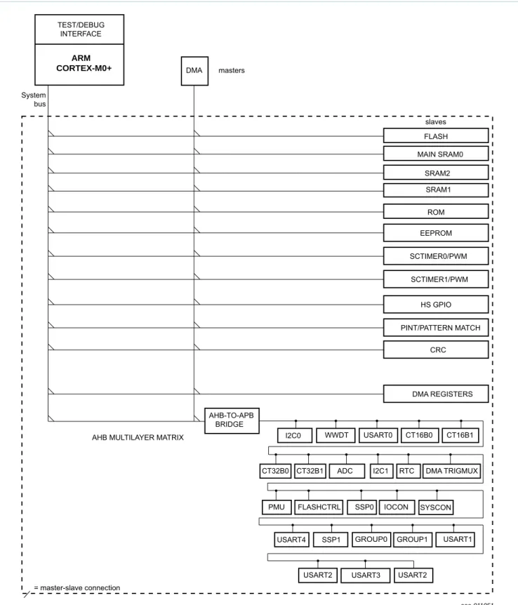
8.2 AHB multilayer matrix
The AHB multilayer matrix supports two masters, the M0+ core and the DMA. All masters can access all slaves (peripherals and memories).
Fig 7. AHB multilayer matrix ARM CORTEX-M0+ TEST/DEBUG INTERFACE DMA AHB-TO-APB BRIDGE EEPROM HS GPIO slaves SRAM1 System bus masters FLASH ROM
AHB MULTILAYER MATRIX
= master-slave connection WWDT USART0 CT32B0 I2C0 FLASHCTRL SSP0 CT32B1 DMA TRIGMUX PMU I2C1 ADC IOCON RTC
GROUP0 GROUP1 USART1
SSP1 USART4 SYSCON MAIN SRAM0 SRAM2 SCTIMER0/PWM SCTIMER1/PWM PINT/PATTERN MATCH CRC DMA REGISTERS CT16B0 CT16B1
USART2 USART3 USART2
8.3 On-chip flash programming memory
The LPC11E6x contain up to 256 KB on-chip flash program memory. The flash can be programmed using In-System Programming (ISP) or In-Application Programming (IAP) via the on-chip bootloader software.
The flash memory is divided into 24 x 4 KB and 5 x 32 KB sectors. Individual pages of 256 byte each can be erased using the IAP erase page command.
8.4 EEPROM
The LPC11E6x contain 4 KB of on-chip byte-erasable and byte-programmable EEPROM data memory. The EEPROM can be programmed using In-Application Programming (IAP) via the on-chip bootloader software.
8.5 SRAM
The LPC11E6x contain a total of up to 36 KB on-chip static RAM memory. The main SRAM block contains either 8 KB, 16 KB. or 32 KB of main SRAM0. Two additional SRAM blocks of 2 KB (SRAM1 and SRAM2) are located in separate areas of the memory map. See Figure 8.
8.6 On-chip ROM
The on-chip ROM contains the bootloader and the following Application Programming Interfaces (APIs):
•
In-System Programming (ISP) and In-Application Programming (IAP) support for flash including IAP erase page command.•
IAP support for EEPROM•
Power profiles for configuring power consumption and PLL settings•
32-bit integer division routines•
APIs to use the following peripherals:– I2C
– USART0 and USART1/2/3/4
– DMA
8.7 Memory mapping
The LPC11E6x incorporates several distinct memory regions, shown in the following figures. Figure 8 shows the overall map of the entire address space from the user program viewpoint following reset. The interrupt vector area supports address remapping. The AHB (Advanced High-performance Bus) peripheral area is 2 MB in size and is divided to allow for up to 128 peripherals. The APB (Advanced Peripheral Bus) peripheral area is 512 KB in size and is divided to allow for up to 32 peripherals. Each peripheral of either type is allocated 16 KB of space. This addressing scheme allows simplifying the address decoding for each peripheral.
8.8 Nested Vectored Interrupt Controller (NVIC)
The Nested Vectored Interrupt Controller (NVIC) is part of the Cortex-M0+. The tight coupling to the CPU allows for low interrupt latency and efficient processing of late arriving interrupts.
Fig 8. LPC11E6x Memory map
APB peripherals 0x4000 4000 0x4000 8000 0x4000 C000 0x4001 0000 0x4001 8000 0x4002 0000 0x4002 8000 0x4003 8000 0x4003 C000 0x4004 0000 0x4004 4000 0x4004 8000 0x4004 C000 0x4005 0000 0x4005 8000 0x4005 C000 0x4006 0000 0x4006 4000 0x4006 C000 0x4007 0000 0x4008 0000 0x4002 4000 0x4001 C000 0x4001 4000 0x4000 0000 WWDT 32-bit counter/timer 0 32-bit counter/timer 1 12-bit ADC USART0 PMU I2C0 20 - 21 reserved 11 - 13 reserved RTC I2C1 30 - 31 reserved 0 1 2 3 4 5 6 7 8 9 0x4002 C000 DMA TRIGMUX 10 16 15 14 17 18 reserved reserved reserved 0x0000 0000 0 GB 0.5 GB 4 GB 1 GB 0x1000 8000 0x1FFF 0000 0x1FFF 8000 0x2000 0000 0x5000 0000 0x5000 4000 0xFFFF FFFF reserved reserved reserved 2 KB SRAM2 reserved 0x4000 0000 0x4008 0000 0x4008 4000 APB peripherals reserved CRC 0x5000 8000 DMA 0x5000 C000 0x5000 E000 SCTIMER0/PWM 0xA000 0000 GPIO 0xA000 4000 0xA000 8000 GPIO PINT 0x5001 0000 SCTIMER1/PWM 0x2000 4000 0x2000 4800 2 KB SRAM1 0x2000 0800
32 KB MAIN SRAM0 (LPC11E68)
0x1000 4000 16 KB MAIN SRAM0 (LPC11E67)
0x1000 2000 8 KB MAIN SRAM0 (LPC11E66)
0x1000 0000 LPC11E6x
0x0004 0000 256 KB on-chip flash (LPC11E68)
0x0002 0000 128 KB on-chip flash (LPC11E67)
0x0001 0000 64 KB on-chip flash (LPC11E66)
32 KB boot ROM 0x1400 0000 0x1400 1000 4 KB MTB registers 0x0000 0000 0x0000 00C0 active interrupt vectors
reserved reserved reserved reserved SSP0 SSP1 16-bit counter/timer 1 16-bit counter/timer 0 IOCON system control (SYSCON)
19 USART4
22
23 GPIO GROUP0 interrupt 24 GPIO GROUP1 interrupt
0x4007 4000 0x4007 8000 USART1 27 28 USART2 29 USART3 25 - 26 reserved flash/EEPROM controller 0xE000 0000 0xE010 0000 private peripheral bus
8.8.1 Features
•
Controls system exceptions and peripheral interrupts.•
In the LPC11E6x, the NVIC supports vectored interrupts for each of the peripherals and the eight pin interrupts. The following peripheral interrupts are ORed to contribute to one interrupt in the NVIC:– USART1, USART4
– USART2, USART3
– SCTimer0/PWM, SCTimer1/PWM
– BOD, WWDT
– ADC end-of-sequence A interrupt, threshold crossing interrupt
– ADC end-of-sequence B interrupt, overrun interrupt
– Flash, EEPROM
•
Four programmable interrupt priority levels with hardware priority level masking.•
Software interrupt generation.8.8.2 Interrupt sources
Each peripheral device has at least one interrupt line connected to the NVIC but can have several interrupt flags. Individual interrupt flags can also represent more than one interrupt source.
8.9 IOCON block
The IOCON block allows selected pins of the microcontroller to have more than one function. Configuration registers control the multiplexers to allow connection between the pin and the on-chip peripherals.
Connect peripherals to the appropriate pins before activating the peripheral and before enabling any related interrupt.
Enabling an analog function disables the digital pad. However, the internal pull-up and pull-down resistors as well as the pin hysteresis must be disabled to obtain an accurate reading of the analog input.
8.9.1 Features
•
Programmable pin function.•
Programmable pull-up, pull-down, or repeater mode.•
All pins (except PIO0_4 and PIO0_5) are pulled up to 3.3 V (VDD = 3.3 V) if theirpull-up resistor is enabled.
•
Programmable pseudo open-drain mode.•
Programmable (on/off) 10 ns glitch filter on pins PIO0_22, PIO0_23, PIO0_11 to PIO0_16, PIO1_3, PIO1_9, PIO1_22, and PIO1_29. The glitch filter is turned on by default.•
Programmable hysteresis.•
Programmable input inverter.•
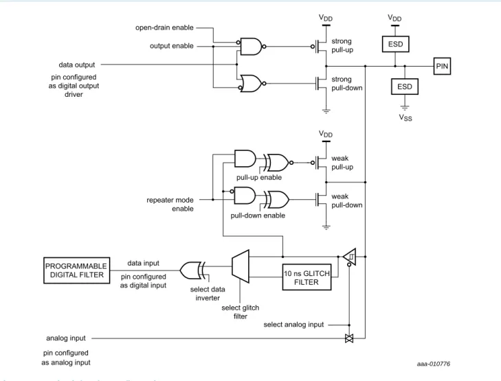
Digital filter with programmable filter constant on all pins. The minimum filter constant is 1/50 MHz = 20 ns.8.9.2 Standard I/O pad configuration
Figure 9 shows the possible pin modes for standard I/O pins with analog input function:
•
Digital output driver with configurable open-drain output•
Digital input: Weak pull-up resistor (PMOS device) enabled/disabled•
Digital input: Weak pull-down resistor (NMOS device) enabled/disabled•
Digital input: Repeater mode enabled/disabled•
Digital input: Input digital filter selectable on all pins. In addition, a 10 ns digital glitch filter is selectable on pins with analog function.•
Analog input8.10 Fast General-Purpose parallel I/O (GPIO)
Device pins that are not connected to a specific peripheral function are controlled by the GPIO registers. Pins may be dynamically configured as inputs or outputs. Multiple outputs can be set or cleared in one write operation.
Fig 9. Standard I/O pin configuration
PIN VDD VDD ESD VSS ESD strong pull-up strong pull-down VDD weak pull-up weak pull-down open-drain enable output enable repeater mode enable pull-up enable pull-down enable select data inverter data output data input select glitch filter analog input
select analog input pin configured as digital output driver pin configured as digital input pin configured as analog input PROGRAMMABLE
DIGITAL FILTER 10 ns GLITCH
FILTER
LPC11E6x use accelerated GPIO functions:
•
GPIO registers are on the ARM Cortex-M0+ IO bus for fastest possible single-cycle I/O timing, allowing GPIO toggling with rates of up to 25 MHz.•
An entire port value can be written in one instruction.•
Mask, set, and clear operations are supported for the entire port.8.10.1 Features
•
Bit level port registers allow a single instruction to set and clear any number of bits in one write operation.•
Direction control of individual bits.8.11 Pin interrupt/pattern match engine
The pin interrupt block configures up to eight pins from all digital pins for providing eight external interrupts connected to the NVIC.
The pattern match engine can be used, in conjunction with software, to create complex state machines based on pin inputs.
Any digital pin except pins PIO2_8 and PIO2_23 can be configured through the SYSCON block as input to the pin interrupt or pattern match engine. The registers that control the pin interrupt or pattern match engine are on the IO+ bus for fast single-cycle access.
8.11.1 Features
•
Pin interrupts– Up to eight pins can be selected from all digital pins except pins PIO2_8 and PIO2_23 as edge- or level-sensitive interrupt requests. Each request creates a separate interrupt in the NVIC.
– Edge-sensitive interrupt pins can interrupt on rising or falling edges or both.
– Level-sensitive interrupt pins can be HIGH- or LOW-active.
– Pin interrupts can wake up the part from sleep mode, deep-sleep mode, and power-down mode.
•
Pin interrupt pattern match engine– Up to 8 pins can be selected from all digital pins except pins PIO2_8 and PIO2_23 to contribute to a boolean expression. The boolean expression consists of
specified levels and/or transitions on various combinations of these pins.
– Each minterm (product term) comprising the specified boolean expression can generate its own, dedicated interrupt request.
– Any occurrence of a pattern match can be programmed to generate an RXEV notification to the ARM CPU as well.
8.12 GPIO group interrupts
The GPIO pins can be used in several ways to set pins as inputs or outputs and use the inputs as combinations of level and edge sensitive interrupts. For each port/pin connected to one of the two the GPIO Grouped Interrupt blocks (GINT0 and GINT1), the GPIO grouped interrupt registers determine which pins are enabled to generate interrupts and the active polarities of each of those inputs.
The GPIO grouped interrupt registers also select whether the interrupt output is level or edge triggered and whether it is based on the OR or the AND of all of the enabled inputs. When the designated pattern is detected on the selected input pins, the GPIO grouped interrupt block generates an interrupt. If the part is in a power-savings mode, it first asynchronously wakes up the part prior to asserting the interrupt request. The interrupt request line can be cleared by writing a one to the interrupt status bit in the control register.
8.12.1 Features
•
Two group interrupts are supported to reflect two distinct interrupt patterns.•
The inputs from any number of digital pins can be enabled to contribute to a combined group interrupt.•
The polarity of each input enabled for the group interrupt can be configured HIGH or LOW.•
Enabled interrupts can be logically combined through an OR or AND operation.•
The grouped interrupts can wake up the part from sleep, deep-sleep or power-downmodes.
8.13 DMA controller
The DMA controller can access all memories and the USART and SSP peripherals using DMA requests. DMA transfers can also be triggered by internal events like the ADC interrupts, timer match outputs, the pin interrupts (PINT0 and PINT1) and the SCTimer DMA requests.
8.13.1 Features
•
16 channels with 14 channels connected to peripheral request inputs.•
DMA operations can be triggered by on-chip events or two of the pin interrupts. Each DMA channel can select one trigger input from 12 sources.•
Priority is user selectable for each channel.•
Continuous priority arbitration.•
Address cache with two entries.•
Efficient use of data bus.•
Supports single transfers up to 1,024 words.8.14 USART0
Remark: The LPC11E6x contains two distinctive types of UART interfaces: USART0 is software-compatible with the USART interface on the LPC11E1x/3x parts. USART1 to USART4 use a different register interface.
The USART0 includes full modem control, support for synchronous mode, and a smart card interface. The RS-485/9-bit mode allows both software address detection and automatic address detection using 9-bit mode.
The USART0 uses a fractional baud rate generator. Standard baud rates such as 115200 Bd can be achieved with any crystal frequency above 2 MHz.
8.14.1 Features
•
Maximum USART0 data bit rate of 3.125 Mbit/s in asynchronous mode and 10 Mbit/s in synchronous slave and master mode.•
16 byte receive and transmit FIFOs.•
Register locations conform to 16C550 industry standard.•
Receiver FIFO trigger points at 1 B, 4 B, 8 B, and 14 B.•
Built-in fractional baud rate generator covering wide range of baud rates without a need for external crystals of particular values.•
Fractional divider for baud rate control, auto baud capabilities and FIFO control mechanism that enables software flow control implementation.•
Support for RS-485/9-bit mode.•
Support for modem control.•
Support for synchronous mode.•
Includes smart card interface.•
DMA support.8.15 USART1/2/3/4
Remark: The LPC11E6x contains two distinctive types of UART interfaces: USART0 is software-compatible with the USART interface on the LPC11E1x/LPC11E3x parts. USART1 to USART4 use a different register interface to achieve the same UART functionality except for modem and smart card control.
Remark: USART4 IS available only on part LPC11E68JBD100.
Interrupts generated by the USART1/2/3/4 peripherals can wake up the part from Deep-sleep and power-down modes if the USART is in synchronous mode, the 32 kHz mode is enabled, or the CTS interrupt is enabled. This wake-up mechanism is not available with the USART0 peripheral.
8.15.1 Features
•
Maximum bit rates of 3.125 Mbit/s in asynchronous mode and 10 Mbit/s in synchronous mode.•
Synchronous mode with master or slave operation. Includes data phase selection and continuous clock option.•
Multiprocessor/multidrop (9-bit) mode with software-address compare feature. (RS-485 possible with software address detection and transceiver direction control.)•
RS-485 transceiver output enable.•
Autobaud mode for automatic baud rate detection•
Parity generation and checking: odd, even, or none.•
One transmit and one receive data buffer.•
RTS/CTS for hardware signaling for automatic flow control. Software flow control can be performed using Delta CTS detect, Transmit Disable control, and any GPIO as an RTS output.•
Received data and status can optionally be read from a single register•
Break generation and detection.•
Receive data is 2 of 3 sample "voting". Status flag set when one sample differs.•
Built-in Baud Rate Generator with auto-baud function.•
A fractional rate divider is shared among all USARTs.•
Interrupts available for Receiver Ready, Transmitter Ready, Receiver Idle, change in receiver break detect, Framing error, Parity error, Overrun, Underrun, Delta CTS detect, and receiver sample noise detected.•
Loopback mode for testing of data and flow control.•
In synchronous slave mode, wakes up the part from deep-sleep and power-down modes.•
Special operating mode allows operation at up to 9600 baud using the 32 kHz RTC oscillator as the UART clock. This mode can be used while the device is inDeep-sleep or Power-down mode and can wake up the device when a character is received.
•
USART transmit and receive functions work with the system DMA controller.8.16 SSP serial I/O controller (SSP0/1)
The SSP controllers operate on an SSP, 4-wire SSI, or Microwire bus. The controller can interact with multiple masters and slaves on the bus. Only a single master and a single slave can communicate on the bus during a given data transfer. The SSP supports full duplex transfers, with frames of 4 bit to 16 bit of data flowing from the master to the slave and from the slave to the master. In practice, often only one direction carries meaningful data.
8.16.1 Features
•
Maximum SSP speed of 25 Mbit/s (master) or 4.17 Mbit/s (slave) (in SSP mode)•
Compatible with Motorola SPI (Serial Peripheral Interface), 4-wire Texas InstrumentsSSI (Serial Synchronous Interface), and National Semiconductor Microwire buses
•
Synchronous serial communication•
Master or slave operation•
4-bit to 16-bit frame•
DMA support8.17 I
2C-bus serial I/O controller
The LPC11E6x contain two I2C-bus controllers.
The I2C-bus is bidirectional for inter-IC control using only two wires: a Serial Clock line
(SCL) and a Serial Data line (SDA). Each device is recognized by a unique address and can operate as either a receiver-only device (e.g., an LCD driver) or a transmitter with the capability to both receive and send information (such as memory). Transmitters and/or receivers can operate in either master or slave mode, depending on whether the chip has to initiate a data transfer or is only addressed. The I2C is a multi-master bus and can be
controlled by more than one bus master connected to it.
8.17.1 Features
•
One I2C-interface (I2C0) is an I2C-bus compliant interface with open-drain pins. TheI2C-bus interface supports Fast-mode Plus with bit rates up to 1 Mbit/s.
•
One I2C-interface (I2C1) uses standard digital pins. The I2C-bus interface supports bitrates up to 400 kbit/s.
•
Easy to configure as master, slave, or master/slave.•
Programmable clocks allow versatile rate control.•
Bidirectional data transfer between masters and slaves.•
Multi-master bus (no central master).•
Arbitration between simultaneously transmitting masters without corruption of serial data on the bus.•
Serial clock synchronization allows devices with different bit rates to communicate via one serial bus.•
Serial clock synchronization can be used as a handshake mechanism to suspend and resume serial transfer.•
The I2C-bus can be used for test and diagnostic purposes.•
The I2C-bus controller supports multiple address recognition and a bus monitor mode.8.18 Timer/PWM subsystem
Four standard timers and two state configurable timers can be combined to create multiple PWM outputs using the match outputs and the match registers for each timer. Each timer can create multiple PWM outputs with its own time base.
The standard timers and the SCTimers combine to up to eight independent timers. Each SCTimer can be configured either as one 32-bit timer or two independently counting 16-bit timers which use the same input clock. The following combinations are possible:
Table 4. PWM resources
PWM outputs
Peripheral Pin functions available for PWM Match registers used LQ FP10 0 LQ FP64 LQ FP48 LQFP100 LQFP64 LQFP48 3 3 3 CT16B0 CT16B0_MAT0, CT16B0_MAT1, CT16B0_MAT2 CT16B0_MAT0, CT16B0_MAT1, CT16B0_MAT2 CT16B0_MAT0, CT16B0_MAT1, CT16B0_MAT2 4 2 2 2 CT16B1 CT16B1_MAT0, CT16B1_MAT1 CT16B1_MAT0, CT16B1_MAT1 CT16B1_MAT0, CT16B1_MAT1 3 3 3 3 CT32B0 three of CT32B0_MAT0, CT32B0_MAT1, CT32B0_MAT2, CT32B0_MAT3 three of CT32B0_MAT0, CT32B0_MAT1, CT32B0_MAT2, CT32B0_MAT3 three of CT32B0_MAT0, CT32B0_MAT1, CT32B0_MAT2, CT32B0_MAT3 4 3 3 3 CT32B1 three of CT32B1_MAT0, CT32B1_MAT1, CT32B1_MAT2, CT32B1_MAT3 three of CT32B1_MAT0, CT32B1_MAT1, CT32B1_MAT2, CT32B1_MAT3 three of CT32B1_MAT0, CT32B1_MAT1, CT32B1_MAT2, CT32B1_MAT3 4 4 4 3 SCTIMER0/ PWM SCT0_OUT0, SCT0_OUT1, SCT0_OUT2, SCT0_OUT3 SCT0_OUT0, SCT0_OUT1, SCT0_OUT2, SCT0_OUT3 SCT0_OUT1, SCT0_OUT2, SCT0_OUT3 up to 5 4 2 - SCTIMER1/ PWM SCT1_OUT0, SCT1_OUT1, SCT1_OUT2, SCT1_OUT3 SCT1_OUT2, SCT1_OUT3 - up to 5
Table 5. Timer configurations
32-bit timers Resources 16-bit timers Resources 4 CT32B0, CT32B1, SCTimer0/PWM
as 32-bit timer, SCTimer1/PWM as 32-bit timer
2 CT16B0, CT16B1
2 CT32B0, CT32B1 6 CT16B0, CT16B1, SCTimer0/PWM
as two 16-bit timers,
SCTimer1/PWM as two 16-bit timers
3 CT32B0, CT32B1, SCTimer0/PWM
as 32-bit timer (or SCTimer1/PWM as 32-bit timer)
4 CT16B0, CT16B1, SCTimer1/PWM
as two 16-bit timers (or SCTimer0/PWM as two 16-bit timers)
8.18.1 State Configurable Timers (SCTimer0/PWM and SCTimer1/PWM)
The state configurable timer can create timed output signals such as PWM outputs triggered by programmable events. Combinations of events can be used to define timer states. The SCTimer/PWM can control the timer operations, capture inputs, change states, and toggle outputs triggered only by events entirely without CPU intervention. If multiple states are not implemented, the SCTimer/PWM simply operates as one 32-bit or two 16-bit timers with match, capture, and PWM functions.
8.18.1.1 Features
•
Each SCTimer/PWM supports:– 5 match/capture registers.
– 6 events.
– 8 states.
– 4 inputs and 4 outputs.
•
Counter/timer features:– Each SCTimer is configurable as two 16-bit counters or one 32-bit counter.
– Counters can be clocked by the system clock or selected input.
– Configurable as up counters or up-down counters.
– Configurable number of match and capture registers. Up to five match and capture registers total.
– Upon match create the following events: interrupt; stop, limit, halt the timer or change counting direction; toggle outputs.
– Counter value can be loaded into capture register triggered by a match or input/output toggle.
•
PWM features:– Counters can be used with match registers to toggle outputs and create time-proportioned PWM signals.
– Up to four single-edge or dual-edge PWM outputs with independent duty cycle and common PWM cycle length.
•
Event creation features:– The following conditions define an event: a counter match condition, an input (or output) condition such as a rising or falling edge or level, a combination of match and/or input/output condition.
– Selected events can limit, halt, start, or stop a counter or change its direction.
– Events trigger state changes, output toggles, interrupts, and DMA transactions.
– Match register 0 can be used as an automatic limit.
– In bidirectional mode, events can be enabled based on the count direction.
– Match events can be held until another qualifying event occurs.
•
State control features:– A state is defined by events that can happen in the state while the counter is running.
– Each event can be assigned to one or more states.
– State variable allows sequencing across multiple counter cycles.
•
SCTimer match outputs (ORed with the general-purpose timer match outputs) serve as ADC hardware trigger inputs.8.18.2 General purpose external event counter/timers (CT32B0/1 and CT16B0/1)
The LPC11E6x includes two 32-bit counter/timers and two 16-bit counter/timers. The counter/timer is designed to count cycles of the system derived clock. It can optionally generate interrupts or perform other actions at specified timer values, based on four match registers. Each counter/timer also includes one capture input to trap the timer value when an input signal transitions, optionally generating an interrupt.
8.18.2.1 Features
•
A 32-bit/16-bit timer/counter with a programmable 32-bit/16-bit prescaler.•
Counter or timer operation.•
One capture channel per timer, that can take a snapshot of the timer value when an input signal transitions. A capture event may also generate an interrupt.•
Four match registers per timer that allow:– Continuous operation with optional interrupt generation on match.
– Stop timer on match with optional interrupt generation.
– Reset timer on match with optional interrupt generation.
•
Up to four external outputs corresponding to match registers, with the following capabilities:– Set LOW on match.
– Set HIGH on match.
– Toggle on match.
– Do nothing on match.
•
The timer and prescaler may be configured to be cleared on a designated capture event. This feature permits easy pulse-width measurement by clearing the timer on the leading edge of an input pulse and capturing the timer value on the trailing edge.•
PWM output function.•
Match outputs and capture inputs serve as hardware triggers for ADC conversions.8.19 System tick timer (SysTick)
The ARM Cortex-M0+ includes a system tick timer (SYSTICK) that is intended to generate a dedicated SYSTICK exception at a fixed time interval (typically 10 ms).
8.20 Windowed WatchDog Timer (WWDT)
The purpose of the WWDT is to prevent an unresponsive system state. If software fails to update the watchdog within a programmable time window, the watchdog resets the microcontroller
8.20.1 Features
•
Internally resets chip if not periodically reloaded during the programmable time-out period.•
Optional windowed operation requires reload to occur between a minimum and maximum time period, both programmable.•
Optional warning interrupt can be generated at a programmable time before watchdog time-out.•
Software enables the WWDT, but a hardware reset or a watchdog reset/interrupt is required to disable the WWDT.•
Incorrect feed sequence causes reset or interrupt, if enabled.•
Flag to indicate watchdog reset.•
Programmable 24-bit timer with internal prescaler.•
Selectable time period from (Tcy(WDCLK)2564) to (Tcy(WDCLK)2244) inmultiples of Tcy(WDCLK)4.
•
The WatchDog Clock (WDCLK) source can be selected from the IRC or the dedicated watchdog oscillator (WDOsc). The clock source selection provides a wide range of potential timing choices of watchdog operation under different power conditions.8.21 Real-Time Clock (RTC)
The RTC resides in a separate always-on voltage domain with battery back-up. The RTC uses an independent oscillator, also located in the always-on voltage domain.
8.21.1 Features
•
32-bit, 1 Hz RTC counter and associated match register for alarm generation.•
Separate 16-bit high-resolution/wake-up timer clocked at 1 kHz for 1 ms resolutionwith a more that one minute maximum time-out period.
•
RTC alarm and high-resolution/wake-up timer time-out each generate independent interrupt requests. Either time-out can wake up the part from any of the low-power modes, including Deep power-down.8.22 Analog-to-Digital Converter (ADC)
The ADC supports a resolution of 12 bit and fast conversion rates of up to 2 MSamples/s. Sequences of analog-to-digital conversions can be triggered by multiple sources. Possible trigger sources are the counter/timer match outputs and capture inputs and the ARM TXEV.
The ADC includes a hardware threshold compare function with zero-crossing detection.
8.22.1 Features
•
12-bit successive approximation analog to digital converter.•
12-bit conversion rate of up to 2 MSamples/s.•
Temperature sensor voltage output selectable as internal voltage source for channel 0.•
Optional automatic high/low threshold comparison and zero-crossing detection.•
Power-down mode and low-power operating mode.•
Measurement range VREFN to VREFP (typically 3 V; not to exceed VDDA voltagelevel).
•
Burst conversion mode for single or multiple inputs.8.23 Temperature sensor
The temperature sensor transducer uses an intrinsic pn-junction diode reference and outputs a CTAT voltage (Complement To Absolute Temperature). The output voltage varies inversely with device temperature with an absolute accuracy of better than ±5C over the full temperature range (40 C to +105 C) for typical samples. The temperature sensor is approximately linear with a slight curvature. The output voltage is measured over different ranges of temperatures and fit with linear-least-square lines.
After power-up and after switching the input channels of the ADC, the temperature sensor output must be allowed to settle to its stable value before it can be used as an accurate ADC input.
For an accurate measurement of the temperature sensor by the ADC, the ADC must be configured in single-channel burst mode. The last value of a nine-conversion (or more) burst provides an accurate result.