TWO-DIMENSIONAL BISMUTH-BASED LAYERED SUPERCELL FOR MULTIFERROISM
A Dissertation by LEIGANG LI
Submitted to the Office of Graduate and Professional Studies Texas A&M University
in partial fulfillment of the requirements for the degree of DOCTOR OF PHILOSOPHY
Chair of Committee, Haiyan Wang Co-Chair of Committee, Xiaofeng Qian Committee Members, Hong Liang
Xinghang Zhang Head of Department, Ibrahim Karaman
May 2017
Major Subject: Materials Science and Engineering
ii ABSTRACT
Room-temperature multiferroics, possessing ferroelectricity and ferromagnetism simultaneously in one phase, hold great promise in miniaturized devices including sensors, actuators, transducers, and multi-state memories. However, single-phase multiferroics are scarce because of the drastically different orbital requirements for ferroelectricity (requiring empty d-orbital) and ferromagnetism (coming from partially filled d-orbitals). Combining two cations possessing ferroelectric and ferromagnetic ordering respectively into one phase is one of the effective routes towards creating single-phase multiferroic materials, such as the Bi-based perovskites BiFeO3 and Bi2FeMnO6. For Bi-based perovskites, the ferroelectricity comes from the high stereochemical activity of the lone-pair electrons of the Bi3+ cation and the B-site cation provides the magnetism. Bi3Fe2Mn2O10+ supercell (BFMO322 SC) is a layered structure with enhanced ferroelectricity and magnetism compared to the conventional pseudocubic Bi2FeMnO6 phase. BFMO322 SC has been fabricated on LaAlO3 (001) substrate and can also be fabricated on CeO2 buffer layer.
In this dissertation, the influence of CeO2 thickness to the growth and magnetic property of BFMO322 SC has been first investigated. The result shows that a CeO2 buffer layer as thin as 6.7 nm is sufficient to trigger the growth of BFMO322 SC and the sample exhibits the best magnetic properties with both highest magnetization and anisotropy. The growth of BFMO322 SC with high phase purity and superior magnetic properties on CeO2
iii
with a thickness of 6.7 nm is attributed to the lattice match between Ce-Ce and Bi-Bi bond as well as the smooth surface of CeO2 buffer layer.
Next, the influence of Fe/Mn molar ratio to the growth and magnetic property of Bi-based layered supercell structure has been studied by both experimental and theoretical methods. It was found that that Mn is more important than Fe in facilitating the growth of Bi-based layered supercell structures. With more Fe than Mn in the structure, the layered supercell structure cannot be formed. The three-dimensional distribution of Young’s modulus of the Bi-based layered supercell structures is calculated based on density functional theory. The theoretical calculation indicates that the strain energy is too high to keep the layered supercell structure if there is more Fe than Mn. In particular, the layered supercell structure with Bi2Ox slabs can also be obtained on CeO2 buffer layer and SrTiO3 (001) for single-perovskite BiMnO3 under well controlled growth conditions.
Then tunable layered supercell (SC) structures have been designed and achieved in both BiMnO3 and Bi2NiMnO6 thin films. More specifically, both supercells with two layer BiOx-slabs (2-Bi SC) and three layer structure BiOx-slabs (3-Bi SC) have been achieved on both LaAlO3 (001) and SrTiO3 (001) under deposition parameter tuning. The novel layered supercell structures consist of alternative layered stacking of Bi2Ox (or Bi3Ox) slabs and Mn-O (or Ni-Mn-O) octahedra layers along out-of-plane direction, respectively. Both the BiMnO3 and Bi2NiMnO6 layered supercell structures exhibit robust multiferroic response at room temperature and tunable ferromagnetic and optical properties attributed to the variable SC structures.
iv
Finally, a new layered supercell structure with Bi3Ox slabs has been designed and fabricated from the new material system Bi2AlMnO6 (BAMO). The new BAMO layered supercell structure is self-assembly grown by alternative layered stacking of three-layer-thick Bi-based slabs [Bi3O3+] and one-layer-thick [MO2]∞ layer (M = Al/Mn). It can be fabricated on single-crystal substrates SrTiO3 (001) and LaAlO3 (001), with or without CeO2 (001) and La0.7Sr0.3MnO3 (001) buffer layers. Robust room-temperature multiferroic responses have been observed for the new BAMO misfit (incommensurate) layered structure with non-magnetic cations Al3+ and magnetic cations Mn3+.
The Bi-based layered supercell structures present great composition flexibility and hold great significance towards the design and creation of new two-dimensional layered materials with a wide range of potential functionalities, such as single-phase multiferroic materials, thermoelectrics, and layered materials with tunable band gaps.
v
DEDICATION
vi
ACKNOWLEDGMENTS
I would like to sincerely thank my research supervisor, Dr. Haiyan Wang, for all her patient and great guidance during my Ph.D. study at Texas A&M University. First, I want to express my appreciation to Dr. Wang for giving me the chance to study in her group. I treasure this great opportunity. The thing that inspires me the most during my study is that she always keeps positive, happy, and enthusiastic to both life and research. Dr. Wang tries her best to provide us the state-of-the-art experimental tools which ensures high-quality research. I want to thank Dr. Wang’s encouragement as well as her great support which helps me discover many interesting things in research. I benefited a lot from Dr. Wang’s strong network in research community. I am also impressed by Dr. Wang’s broad knowledge in both materials science and experimental skills. I also appreciate Dr. Wang’s great support and guidance to my personal life. I feel I am very lucky to pursue my Ph.D. study in Dr. Wang’s group.
I would like to acknowledge all my thesis committee members, Dr. Xiaofeng Qian, Dr. Hong Liang, and Dr. Xinghang Zhang for their great help and attention to my research. I am thankful for their great efforts to my preliminary exam and final defense.
I want to thank my former and present group members, Dr. Aiping Chen, Dr. Qing Su, Dr. Wenrui Zhang, Dr. Fauzia Khatkhatay, Dr. Clement Jacob, Dr. Liang Jiao, Dr. Jie Jian, Dr. Jijie Huang, Meng Fan, Han Wang, Xuejing Wang, Xingyao Gao, Bruce Zhang, and Zhimin Qi for their camaraderie and collaboration.
vii
I also want to acknowledge the faculty and staff at the Microscopy and Imaging Center as well as the Materials Characterization Facility at Texas A&M for their help and advice with equipment training.
Finally, I would like to thank all my families for their great support during all my Ph.D. study. Without their encouragement and support, I could not reach this far.
viii
CONTRIBUTORS AND FUNDING SOURCES
Contributors
This work was supported by a dissertation committee consisting of Professor Haiyan Wang (Chair) of the Department of Electrical and Computer Engineering and Xiaofeng Qian (Co-Chair) of the Department of Materials Science and Engineering and Professors Hong Liang and Xinghang Zhang of the Department of Mechanical Engineering.
Jie Jian from Texas A&M University was thanked for his help in taking high-resolution STEM images. Xingyao Gao, Xuejing Wang, and Bruce Zhang from Texas A&M University were thanked for their help in preparing TEM samples. I would like to thank Dr. Ping Lu at Sandia National Laboratories for his great support in STEM imaging and EDS mapping, Dr. Philippe Boullay, Dr. Olivier Perez, and Gwladys Steciuk from France for their great help in constructing the crystal structures, and Dr. Xiaofeng Qian and Hua Wang for their assistance in first-principles calculations. All other work conducted for the dissertation was completed by the student independently.
Funding Sources
Graduate study was supported by China Scholarship Council (CSC), U.S. Office of Naval Research and U.S. National Science Foundation.
ix
NOMENCLATURE
PVD Physical Vapor Deposition
CVD Chemical Vapor Deposition
MBE Molecular Beam Epitaxy
PLD Pulsed Laser Deposition
DC Direct Current
RF Radio Frequency
APCVD Atmospheric Pressure CVD
LPCVD Low-Pressure CVD
PECVD Plasma-Enhanced CVD
ALCVD Atomic Layer CVD
MOCVD Metal-Organic CVD
Ps Saturation Polarization
Pr Remanent Polarization
Ec Electric Coercive Field
Es Electric Switching Field
TC Curie Temperature
CMR Colossal Magnetoresistance
T Tesla
oC Degree Centigrade
x
t Goldschmidt Tolerance Factor
GK Goodenough-Kanamori
B Bohr Magneton
PFM Piezoelectric Force Microscopy
XRD X-ray Diffraction
Oe Oersted
TN Antiferromagnetic Neel Temperature
emu/cc Magnetic Moment/Cubic Centimeter
kOe Kilo-Oersted
SQUID Superconducting Quantum Interference Device XMCD X-ray Magnetic Circular Dichroism
f.u. Formula Unit
TEM Transmission Electron Microscope
GPA Geometric Phase Analysis
BF Bright-Field
DF Dark-Field
STEM Scanning Transmission Electron Microscopy
ADF Annular Dark-Field
HAADF High-Angle Annular Dark-Field
EDS Energy-Dispersive X-ray Spectroscopy
VSM Vibrating Sample Magnetometer
xi
M Magnetization
T Temperature
FC Field Cooling
ZFC Zero-Field Cooling
PED Precession Electron Diffraction
ABF Annular Bright-Field
AFM Atomic Force Microscopy
XPS X-ray Photoelectron Spectroscopy
PEDT Precession Electron Diffraction Tomography
xii TABLE OF CONTENTS Page ABSTRACT ...ii DEDICATION ... .v ACKNOWLEDGMENTS ...vi CONTRIBUTORS AND FUNDING SOURCES ...viii NOMENCLATURE ... ix
TABLE OF CONTENTS ...xii LIST OF FIGURES ... xv
LIST OF TABLES ... xxv
CHAPTER I INTRODUCTION ... 1
1.1 Functional metal oxide thin films ... 1
1.1.1 Overview of functional metal oxides ... 1
1.1.2 Crystal structures of functional metal oxides ... 2
1.1.3 Growth of metal oxide thin films ... 5
1.2 Functionalities of oxide thin films ... 13
1.2.1 Ferroelectricity ... 13
1.2.2 Magnetism ... 18
1.2.3 Multiferroism ... 24
1.3 Bismuth-based perovskites for multiferroism ... 30
1.3.1 Overview of perovskites ... 30
1.3.2 BiFeO3 ... 35
1.3.3 BiMnO3 ... 42
1.3.4 Bi2FeMnO6 ... 50
1.3.5 Bi2NiMnO6 ... 56
1.4 Two-dimensional layered materials ... 60
1.4.1 Overview of two-dimensional materials ... 60
1.4.2 Non-oxide based two-dimensional layered materials ... 61
1.4.3 Oxide-based two-dimensional layered materials ... 63
1.5 Research motivation ... 74
xiii
2.1 Pulsed laser deposition ... 76
2.2 Microstructure characterization ... 82
2.2.1 X-ray diffraction ... 82
2.2.2 Transmission electron microscopy ... 83
2.2.3 Scanning transmission electron microscopy ... 88
2.2.4 Energy-dispersive X-ray spectroscopy ... 91
2.2.5 TEM sample preparation ... 91
2.3 Physical property measurement ... 92
2.3.1 Magnetic property measurement ... 92
2.3.2 Electrical property measurement ... 93
2.4 Precision electron diffraction tomography ... 94
CHAPTER III STRAIN AND INTERFACE EFFECTS IN A NOVEL BISMUTH-BASED SELF-ASSEMBLED SUPERCELL STRUCTURE ... 96
3.1 Overview ... 96
3.2 Introduction ... 97
3.3 Experimental ... 99
3.4 Results and discussion ... 100
3.5 Conclusion ... 111
CHAPTER IV TUNABLE PHYSICAL PROPERTIES IN TWO-DIMENSIONAL BI-BASED LAYERED SUPERCELL STRUCTURES VIA COMPOSITION VARIATION………..113
4.1 Overview ... 113
4.2 Introduction ... 113
4.3 Experimental details and first-principle calculation ... 115
4.4 Results and discussion ... 117
4.5 Conclusion ... 129
CHAPTER V TWO-DIMENSIONAL LAYERED SUPERCELLS FROM BIMNO3 AND BI2NIMNO6: SELF-ASSEMBLED GROWTH, STRUCTURE MODULATION, AND TUNABLE PHYSICAL PROPERTIES ... 130
5.1 Overview ... 130
5.2 Introduction ... 131
5.3 Experimental ... 133
5.4 Results and discussion ... 135
5.5 Conclusion ... 159
CHAPTER VI SELF-ASSEMBLED LAYERED SUPERCELL STRUCTURE OF BI2ALMNO6 WITH STRONG ROOM-TEMPERATURE MULTIFERROIC PROPERTIES ... 161
xiv
6.1 Overview ... 161
6.2 Introduction ... 161
6.3 Experimental ... 164
6.4 Results and discussion ... 166
6.5 Conclusion ... 187
CHAPTER VII SUMMARY AND FUTURE WORK ... 189
xv
LIST OF FIGURES
Page Figure 1.1 Common binary oxide crystal structures including (a) rocksalt, (b)
wurzite, (c) fluorite, (d) rutile, and (e) corundum……….………….…...……4 Figure 1.2 Common ternary oxide crystal structures including (a) ilmentite, (b)
spinel, (c) perovskite, and derivatives of the perovskite such as
(d) Ruddlesden-Popper series, and (e) layered perovskites………...………4 Figure 1.3 Schematic illustration of (a) lattice-matched epitaxy, (b) coherently
strained lattice-mismatched heteroepitaxy, and (c) relaxed
lattice-mismatched heteroepitaxy...…10 Figure 1.4 HRTEM and fast Fourier filtered images of domain matching epitaxy of
SrTiO3 thin film grown on MgO substrate with a 14/13 matching……….….12 Figure 1.5 Ferroelectric polarization-electric field hysteresis loop corresponding to
two lattice distortions, polarization up and polarization down………...15 Figure 1.6 Temperature-dependent unit cell dimensions, spontaneous polarization,
and dielectric constant of BaTiO3………..…….16 Figure 1.7 Oxygen pressure dependent (a) Ti/Ba ratio and (b) Pr in BaTiO3 films………18 Figure 1.8 Schematic diagram showing the spin alignment for different magnetism……21 Figure 1.9 Schematic diagram showing the magnetic couplings in oxides.
(a) superexchange, (b) double exchange, and (c) RKKY coupling……….…21 Figure 1.10 Magnetoresistance ratio (ΔR/RH) versus temperature curves for the
La-Ca-Mn-O films treated under different conditions: curve 1, as deposited; curve 2, annealing at 700 oC in O2 for 30 min; curve 3,
annealing at 900 oC in O2 for 3 hours……….…….24 Figure 1.11 A schematic showing the relationship between ferroelectricity,
magnetism, and multiferroism……….………..26 Figure 1.12 Schematic diagrams showing the three types of multiferroic materials:
(a) single-phase epitaxial thin films, (b) horizontal multilayered
heterostructures, and (c) vertically aligned heterostructures……….….27 Figure 1.13 (a) Crystal structures of YMnO3 with paraelectric and ferroelectric
xvi
Page phases. (b) polarization-electric field hysteresis of the epitaxial
YMnO3/Pt and the oriented-YMnO3/Pt………...……….29 Figure 1.14 The charge-ordering model for RFe2O4 showing the double iron layer……..30 Figure 1.15 A schematic showing the superexchange interaction in ABO3 perovskite
with 180o B-O-B bond angle. The magnetic interaction can be either antiferromagnetic (a, b) or ferromagnetic (c) depending on the
occupation of eg orbitals………..………..………….34 Figure 1.16 Crystal structure of BiFeO3 from different orientations: (a)
pseudocubic-[110], (b) pseudocubic-[111], and (c) a general three dimensional view of the structure. (d) The magnetic structure
of BiFeO3………..………...………..36
Figure 1.17 (a) Schematic diagrams showing the heterostructures
of BiFeO3/SrRuO3/DyScO3. (b) Domain structure of BFO thin film predicted by phase field simulations. The in-plane PFM images of domain structures in BFO thin films showing (c) 4-polarization variants (left), and 2-polarization variants (right)………38 Figure 1.18 (a) A pseudo-phase diagram demonstrating the structural and
property evolution of Ca-doped BiFeO3. (b) Conducting-atomic
force microscopy image showing an electrically poled and re-poled area of the doped BiFeO3 film. (c) Illustration of the process of creating a
multi-state memory………....39 Figure 1.19 (a) Magnetic hysteresis loops of a 70 nm BFO thin film (blue: in-plane,
red: out-of-plane). (b) Ferroelectric hysteresis loop of BFO thin film……....40 Figure 1.20 X-ray photoemission electron microscopy images before (a) and after
(b) poling. In-plane piezoelectric force microscopy (PFM) images before (c) and after (d) poling. (e) A superposition of in-plane PFM scans shown in (c) and (d) used to identify the different switching
mechanisms that appear with different colors and are labeled in the figure…41 Figure 1.21 XRD θ-2θ scans of Bi-Mn-O thin films deposited on SrTiO3 (001)
substrates at 650 oC under an oxygen pressure range of 1 and 20 mTorr……46 Figure 1.22 (a) XRD θ-2θ pattern for the BiMnO3 thin film grown on SrTiO3 (001).
Inset shows the rocking curve for a (010) BiMnO3 peak. (b) X-ray reciprocal space mapping around the SrTiO3 (114) plane shows well-developed peaks for BiMnO3 in the lower region and two strong
xvii
Page substrate peaks in the upper region………...…..47 Figure 1.23 (a) XRD θ-2θ scans of undoped-BMO and BSMO films. (b)
Normalized magnetization-temperature curve of undoped-BMO and
BSMO thin films under a magnetic field of 200 Oe………..…..49 Figure 1.24 Phase diagram for BiFe1-xMnxO3. The open circles stand for
the antiferromagnetic TN and the closed ones are for ferromagnetic TC……..51 Figure 1.25 (a) Magnetic hysteresis loops of BFO and BFMO thin films along the
out-of-plane direction at room temperature. (b) Magnetic hysteresis loops of BFMO thin films along the in-plane and
out-of-plane directions.………..53 Figure 1.26 (a) XRD θ-2θ scans and (b) ω-rocking curves of BFMO thin films: Film
2 (30 nm thick), Film 3 (60 nm thick), Film 4 (120 nm thick). (c) Normalized in-plane M-T curves of Film 2 and Film 3. (d) The
relationship between c-axis lattice parameter (open squares), FWHM of ω-rocking curves (red squares), and film thickness………55 Figure 1.27 (a) Polarization-electric field loops and (b) magnetization hysteresis
loops of BFMO thin films………..…....56 Figure 1.28 A schematic diagram showing the double-perovskite structure with
long-range B-site order in a rock-salt configuration………...…57 Figure 1.29 (a) Temperature dependence of relative dielectric constant and (b)
temperature dependences of magnetic susceptibility and inverse
susceptibility of Bi2NiMnO6………...…58 Figure 1.30 XRD θ-2θ scans of BLNMO thin films grown (a) at 0.5 mbar of O2 at
different temperatures and (b) at 620 oC at different oxygen pressures...60 Figure 1.31 Crystal structure model of (a) graphene, (b) MoS2, (c) BN, and (d) MB2…....63 Figure 1.32 Crystal structure model of (a) LiCoO2, (b) VO2, (c) YBa2Cu3O7, and
(d) Bi2WO6……….65
Figure 1.33 A perspective drawing of the undistorted patent structures: (a) Bi4Ti3O12 (m = 3), (b) Bi3TiNbO9 (m = 2), and (c) Bi2WO6 (m = 1). (011) sections of (d) Bi2WO6, (e) Bi3TiNbO9, and (f) Bi4Ti3O12 real
xviii
Page Figure 1.34 (a) XRD θ-2θ scan and (b) pole figure of an almost purely a
axis-oriented BLT thin film. (c) Polarization-electric field hysteresis
loop of a Pt/BLT (100)-SrRuO3 (110) capacitor…….………..…..71 Figure 1.35 (a) Scanning electron microscopy image showing that CFO is well
dispersed in the BTFO matrix throughout the entire sample. (b) TEM images showing that the nanopillars grow vertically to the bottom of the matrix. (c) In-plane magnetic hysteresis loops measured at 10 K for BTFO and BTFO/CFO nanocomposite (30 vol.% CFO). (d)-(g)
In-plane piezoelectric force microscopy (PFM) images for four compositions where the volume fraction of the CFO is
systematically increased (d, 5%; e, 20%; f, 35%; and g, 45%)………...72 Figure 1.36 Cross-sectional scanning transmission electron microscopy (STEM)
images of the BFMO322 SC structure grown on (a) LaAlO3 (001) and (c) CeO2 buffered STO substrate. (b) Magnetization hysteresis loops of the BFMO322 SC structure and the pseudocubic Bi2FeMnO6 phase.
(d) Magnified STEM image of the BFMO322 SC structure………..….74 Figure 2.1 Schematic diagram showing the pulsed laser deposition system……….…….77 Figure 2.2 Schematic diagram showing the laser-target interaction stages during the
short pulsed laser process………....………...79 Figure 2.3 Schematic showing the Bragg diffraction for a set of crystal planes………….83 Figure 2.4 Objective aberration: spherical (a), chromatic (b), astigmatism (c)……… ….86 Figure 2.5 The two basic operation modes of the TEM system: (a) diffraction mode
and (b) image mode. In each case the intermediate lens selects either the back focal plane or the image plane of the objective lens as its objects…...…87 Figure 2.6 Schematic diagram showing the (a) bright-field and (b) dark-field
imaging modes………...…88 Figure 2.7 Comparison of the use of an objective aperture in TEM to select (A) the
direct of (B) the scattered electrons form BF and DF images,
respectively. In STEM an on-axis detector (C) or an annular detector is used to form BF or DF images………90 Figure 2.8 (a) The Quantum Design PPMS equipment in the laboratory. (b) The
xix
Page Figure 2.9 Schematic of piezoelectric response measurement in contact mode AFM…...94 Figure 3.1 (a) XRD θ-2θ scans of BFMO film directly grown on STO substrate
with a pseudocubic structure. The “#” indicates impurity phase and PC means pseudocubic phase. (b)-(d) XRD scans of the BFMO322 SC structure grown on STO substrates buffered by different thicknesses of CeO2 ranging from 6.7 nm, 11.5 nm, to 50.0 nm, respectively. The
“*” indicates a minor phase Bi25FeO40….. ………..…101 Figure 3.2 Cross-sectional STEM image of the 6.7 nm CeO2 buffered BFMO322
SC with low magnification (a) and high magnification (b), STEM image of the interface between BFMO322 SC and CeO2 (c), schematic model showing the interface lattice matching between BFMO322 SC and CeO2 (c), schematic model showing the interface lattice matching between BFMO322 SC and CeO2 (d)………...103 Figure 3.3 Cross-sectional TEM images and diffraction patterns of the BFMO
samples (along (100) zone axis). (a) BFMO with pseudocubic structure. (b)-(d) BFMO322 SC structure with the CeO2 thickness of
6.7 nm, 11.5 nm, and 50.0 nm, respectively……….105 Figure 3.4 Cross-sectional TEM image of 11.5 nm CeO2 buffered BFMO sample…….107 Figure 3.5 Cross-sectional TEM image of 50.0 nm CeO2 buffered BFMO sample…….108 Figure 3.6 Room-temperature magnetic properties of the BFMO films. (a)
Out-of-plane (OP) and in-plane (IP) magnetic hysteresis loops of the BFMO film with pseudocubic structure. (b)-(d) OP and IP magnetic hysteresis loops of the BFMO322 SC structure grown on STO substrates buffered by different thicknesses of CeO2 ranging from 6.7
nm, 11.5 nm, to 50.0 nm, respectively………..……111 Figure 4.1 XRD θ-2θ scans of BFMO thin films with different Fe/Mn molar ratios,
1:1 (F1M1), 1:2 (F1M2), 1:4 (F1M4), and 0:1 (F0Mall). The “” indicates a minor phase Bi25FeO40……….………...…..117 Figure 4.2 XRD θ-2θ scans of BFMO thin films with different BFO and BMO
molar ratios, 1:1 (F1M1), 2:1 (F2M1), 4:1 (F4M1), and 1:0 (FallM0)……...118 Figure 4.3 Cross-sectional low-magnification STEM images of (a) F1M1, (d) F1M4,
and (g) F0Mall. High-magnification STEM images of (b) F1M1, (e) F1M4, and (h) F0Mall. The corresponding selected area electron diffraction patterns of (c) F1M1, (f) F1M4, and (i) F0Mall grown on
xx
Page CeO2 buffered STO substrates……….……120 Figure 4.4 XRD θ-2θ scans of F0Mall (a) and F1M1 (b) grown on STO substrate
directly. The symbol “” indicates minor unknown phases. TEM images of F0Mall (c) and F1M1 (d) directly grown on STO. The insets are the corresponding diffraction patterns of layered F0Mall (c) and
pseudocubic F1M1 (d)………..…123
Figure 4.5 Visualization of Young’s modulus of F1M1 layered supercell structure
in unit KBar……….…….126 Figure 4.6 Tunable physical properties of the BFMO thin films with
different compositions and structures. (a) Magnetic hysteresis (M-H) loops of F1M1, F1M2, F1M4 and F0Mall at 300 K along the
out-of-plane direction. (b) Variation of saturation magnetization and coercivity of F1M1, F1M2, F1M4 and F0Mall with different Mn contents. (c) and (d) Tunable transmittance and band gaps of
pseudocubic BFMO, F1M1, F1M2, F1M4 and F0Mall………...…..128 Figure 5.1 XRD patterns of the self-assembled BMO layered supercell structures.
θ-2θ scans of BMO HLSC grown on (a) LAO (001), (c) STO (001), and (e) CeO2-buffered STO (001) substrates, respectively. θ-2θ scans of BMO LLSC grown on (b) LAO (001), (d) STO (001), and (f)
CeO2-buffered LAO (001) substrates, respectively……….…….137 Figure 5.2 XRD θ-2θ patterns of the BNMO thin films with novel layered
supercell structures and conventional pseudocubic structure. Typical θ-2θ scans of the BNMO thin films deposited on LAO (001) and STO (001) substrates at (a) high temperature and (b) low temperature, respectively. HLSC and LLSC mean high-temperature and low -temperature layered supercell, respectively, while PC indicates
the pseudocubic structure. The “” indicates a minor phase Bi12MnO20..…139 Figure 5.3 Microstructural characterization of the BMO layered supercell structures.
(a) and (d) STEM HAADF images of BMO HLSC and LLSC along LAO [100] zone axis, respectively. The inset shows the
corresponding selected area electron diffraction patterns of BMO HLSC and LLSC, respectively. (b) and (f) High-resolution STEM images of BMO HLSC and LLSC taken from the LAO [100] and [110] zone axis, respectively, showing the Bi atoms at atomic
resolution. (c) and (e) High-resolution STEM images of BMO HLSC and LLSC taken from the LAO [110] and [100] zone axis,
xxi
Page Figure 5.4 Microstructural characterization of the two new BNMO LSC. (a) and
(b) HAADF STEM images of BNMO HLSC and LLSC along LAO [100] zone axis, respectively. The insets on the top right corner and bottom right corner in both (a) and (b) are the SAED pattern and high-resolution HAADF STEM image on atomic scale, respectively. (c) and (d) High-resolution HAADF STEM images of BNMO HLSC and LLSC along [100] and [110] zone axis, respectively. (e) and (g) EDS composite color mapping and X-ray profiles for Bi, Ni/Mn, La and Al along the horizontal axis for BNMO HLSC. (f) EDS mapping of Bi (L+M), Ni/Mn (K), La (K), Al (K), and composite color mapping for BNMO LLSC. (h) X-ray profiles for Bi, Ni/Mn, La and
Al along the horizontal axis for BNMO LLSC……….144 Figure 5.5 Reciprocal space electron diffraction tomography (EDT) investigation
of the BNMO LLSC. (a) and (b) Selected EDT patterns showing the sublattice 1 (in green) and sublattice 2 (in red). The sublattice 1 exhibits sharp reflections while the sublattice 2 is disordered with the presence of diffuse scattering lines along [001]*. (c) (hk0)*
plane reconstructed from the EDT experiment performed by collecting patterns in zone with [001]*. Modulation vector
q1=1.a2*+2.b2* relating the sublattice 1 to the sublattice 2………..…….146 Figure 5.6 Structural analysis for BNMO LLSC. (a) High-resolution
HAADF-STEM image of BNMO LLSC showing the in-plane shifts and out-of-plane mirroring of Bi-based slabs. The BNMO LLSC is composed of layered stacking of [Bi3O3+] and [MO2] along the out-of-plane direction. (c) Fourier transform of the larger area STEM -HAADF image (b) showing the disorder related to the Bi-based
stacking (sublattice 2)……….………….147 Figure 5.7 Room-temperature multiferroic properties of the 2D BMO layered
supercell structures. In-plane (IP) and out-of-plane (OP)
magnetization hysteresis (M-H) loops of the BMO (a) HLSC and (b) LLSC at 300 K. (c) Phase and (d) amplitude switching curves of the
BMO HLSC as a function of the tip bias at room temperature...149 Figure 5.8 Magnetizations of BMO (a) HLSC and (b) LLSC as a function of
temperature cooled under zero magnetic field (ZFC) and an in-plane
magnetic field of 1000 Oe (FC), respectively………...…………150 Figure 5.9 The XPS spectra of (a) and (c) Bi 4f; (b) and (d) Mn 2p3/2 for BMO
xxii
Page Figure 5.10 Room-temperature multiferroic properties of the 2D BNMO LSC.
Magnetization hysteresis (M-H) loops of the BNMO (a) HLSC and (b) LLSC at 300 K along both in-plane (IP) and out-of-plane (OP)
directions. (c) Phase and (d) amplitude switching curves of the BNMO LLSC as a function of the tip bias at room temperature showing
the ferroelectric domain switching behavior………152 Figure 5.11 (a) and (c) Temperature-dependent magnetizations of BNMO HLSC
and LLSC at 10 K, 100 K and 300 K along the in-plane direction, respectively. (b) and (d) Magnetizations of BNMO HLSC and LLSC as a function of temperature cooled under zero magnetic field (ZFC)
and an out-of-plane magnetic field of 1000 Oe (FC), respectively……...…154 Figure 5.12 The XPS spectra of (a) and (c) Ni 2p3/2; (b) and (d) Mn 2p3/2 for BNMO
HLSC and LLSC, respectively……….………156 Figure 5.13 Tunable physical properties of the BMO and BNMO thin films with
different structures. (a) Saturation magnetization, (b) Coercivity,
(c) Transmittance, and (d) Band gaps………...………157 Figure 6.1 XRD patterns of the self-assembled BAMO layered supercell structure.
θ-2θ scans of BAMO layered thin films fabricated on LAO (a), STO (b), LSMO-buffered STO (c), and CeO2-buffered STO (d)
substrates, respectively………167 Figure 6.2 Microstructural charaterization of the BAMO layered supercell structure.
(a) STEM HAADF image of BAMO LSC along the STO [100] zone axis. The inset shows the SAED pattern. (b-c) High-resolution STEM HAADF (b) and ABF (c) images showing the layered oxide supercell with a three-atom-thick Bi-based slab and one single Al/Mn based layer. (d) EDS profile showing Bi, Al and Mn along the [001] direction. (e) AFM surface topography image indicating the high
surface quality of the BAMO LSC……….…………..………168 Figure 6.3 (a) STEM HAADF image of BAMO LSC along the LAO [100] zone
axis. (b) Selected area electron diffraction pattern of the BAMO LSC
grown on LAO (100) substrate……….………169 Figure 6.4 Reciprocal space PEDT investigation of the BAMO layered supercell
structure. (a) (hk0)* plane reconstructed from the PEDT
experiment performed by collecting patterns in zone with [001]*. (b) Modulation vector q1=1.a2*+2.b2* relating the sublattice 1 to the sublattice 2. (c) Selected PEDT patterns showing the sublattices 1
xxiii
Page (in green) and 2 (in red). The sublattice 1 exhibits sharp reflections
while the sublattice 2 is disordered with the presence of diffuse scattering lines along [001]*. (d) (h0l)* reciprocal space section reconstructed for the sublattice 1 where the R-centering is evidenced. In this section, the sublattice 2 (in red) is almost not visible but the
satellites reflections/diffuse lines (black arrows) are strong……….…172 Figure 6.5 Structural models for the BAMO layered system. Details of a STEM
-HAADF [100]STO/[100]sublattice2 image showing two consecutive blocks of the three-layer-thick Bi-based subsystem. In (a) Bi atoms face each other from one block to the other. This situation is well reproduced with our first model (c2 = 39.4 Å). In (b) Bi atoms are shifted by 1/3 along b. This situation is well reproduced with our second model (c2 = 78.8 Å). Along this [100]STO direction, the [MO2] layers (sublattice 1),
represented in green, does not project along a direction permitting to resolve the M-M distances. (c) Fourier transform of the larger area STEM-HAADF image showing the disorder related to the Bi-based
stacking (sublattice 2)……….….174 Figure 6.6 Crystal structure model 1 for BAMO misfit layered structure. In this
model, Bi atoms face each other from one block to the other………178 Figure 6.7 Crystal structure model 2 for BAMO misfit layered structure. Bi atoms
are shifted by 1/3 along b from one block to the other………...…...179 Figure 6.8 The XPS spectra of (a) Bi 4f, (b) Al 2p, and (c) Mn 2p3/2 for the
BAMO LSC……….…181 Figure 6.9 Room-temperature multiferroic properties of the 2D BAMO LSC. (a)
In-plane (IP) and out-of-plane (OP) magnetization hysteresis (M-H) loops of the BAMO LSCat 300 K. (b) Temperature-dependent
magnetizations of the BAMO LSC at 10 K, 100 K and 300 K along the in-plane direction. (c) Phase and (d) amplitude switching curves of the BAMO LSC as a function of the tip bias at room temperature. PFM OP (e) phase and (f) amplitude images of the BAMO LSC after +6 V writing over an area of 0.8 0.8 m2 followed by a 0.4 0.4 m2
central area rewriting with the tip biased at -6 V, respectively………..183 Figure 6.10 Magnetizations of BAMO LSC as a function of temperature cooled
under zero magnetic field (ZFC) and an out-of-plane magnetic field of 1000 Oe (FC), respectively………..………185 Figure 6.11 Transmission spectrum of BAMO LSC (a) and plot of (h)2 versus
xxiv
Page h for BAMO LSC (b). The optical band gap energy Eg is deduced
xxv
LIST OF TABLES
Page Table 1.1 The classification of metal oxides………..………..3 Table 1.2 Comparison of different categories of thin film deposition techniques…..……..6 Table 1.3 Crystal structure information and phase transitions of BiMnO3………...……..42 Table 1.4 Phases and compositions of Bi2FeMnO6 films grown on SrTiO3 (001)
substrates at 680 oC and various oxygen partial pressures……….….53 Table 1.5 Crystal information and phase transitions of double
-perovskite Bi2NiMnO6……….59
Table 1.6 Examples of reported Aurivillius phases………..…….66 Table 6.1 Cation ratio in the BAMO LSC with the STO substrate ratio as
a reference………..…..170 Table 6.2 Positional parameters of the misfit layered BAMO structure (model 1). …….174 Table 6.3 Positional parameters of the misfit layered BAMO structure (model 2).…….176
1 CHAPTER I INTRODUCTION
Complex oxide materials have been extensively studied because of their various crystal structures, multifunctionalities and potential device applications. In this chapter, functional metal oxides will be reviewed first in section 1.1, including crystal structures of oxides and oxide thin film growth. Then in section 1.2 the functionalities of oxide thin films including ferroelectricity, magnetism and multiferroism are introduced. In section 1.3, several well-known multiferroic materials are briefly reviewed. In section 1.4, two-dimensional materials including non-oxide based and oxide-based two-two-dimensional materials will be reviewed and finally the research motivation for this work is introduced.
1.1 Functional metal oxide thin films 1.1.1 Overview of functional metal oxides
Metal oxides, especially transition metal oxides, represent a large family of materials that cover a wide range of crystal structures and functionalities. Metal oxides have found various applications and have played an incredible role in modern technology. Oxides with high ferroelectric response and dielectric constant such as BaTiO3 and Pb(Zr,Ti)O3 have been used for tranducers, capacitors, sensors, thermistors, etc.1, 2 Superconductors (e.g. YBa2Cu3O7 and FeSe) have been extensively studied and the proposed applications include superconducting cables, superconducting transformers, and superconducting filters.3, 4 The Li-based metal oxides (e.g. LiCoO
2
layered structures have been commercialized and used as cathode materials in Li-ion batteries.5, 6 Single phase multiferroic materials including BiFeO
3 and BiMnO3 have been extensively studied for the application of data storage.7
Compared to their bulk forms, metal oxides in thin film form have remarkably different crystalline quality and physical properties. With the development of high-quality thin film growth techniques and characterization capabilities, the field of functional metal oxides has experienced unprecedented development in terms of discovering new materials, understanding of fundamental physics, and controlling of physical properties.8 The increasing needs for miniature devices with small volume and low energy consumption have also stimulated the study of functional metal oxide thin films.
1.1.2 Crystal structures of functional metal oxides
As mentioned above, metal oxides have been extensively studied with a wide range of crystal structures and fascinating properties. To understand metal oxides especially their physical properties, one should have solid knowledge of the crystal structures of various oxides. Metal oxides are ionically bonded and can be categorized to binary and ternary oxides as shown in Table 1.1. Binary oxides cover a series of crystal structures including rock salt, fluorite, wurtzite, rutile and corundum (Figure 1.1). The ternary systems include perovskite, spinel, ilmenite, Ruddlesden-Popper, and layered-perovskite (Figure 1.2).
3 Table 1.1 The classification of metal oxides.
Systems Crystal structures Representative oxides
Binary oxides Rock salt MgO, TiO, VO, MnO,
NiO
Wurtzite ZnO, BeO
Fluorite CeO2, ZrO2, HfO2, ThO2 Rutile TiO2, MoO2, RuO2 Corundum Al2O3, V2O3, Cr2O3
Ternary oxides Perovskite CaTiO3, BiFeO3,
SrRuO3
Spinel CoFe2O4, NiFe2O4, MgAl2O4
Ilmenite FeTiO3, MnTiO3, LiNbO3
Layered perovskite YBa2Cu3O7
Ruddlesden-Popper SrRuO3, Sr2RuO4, Sr3Ru2O7
4
Figure 1.1 Common binary oxide crystal structures including (a) rocksalt, (b) wurzite, (c) fluorite, (d) rutile, and (e) corundum.8
Figure 1.2 Common ternary oxide crystal structures including (a) ilmentite, (b) spinel, (c) perovskite, and derivatives of the perovskite such as (d) the Ruddlesden-Popper series, and (e) layered perovskites.8
Among the binary and ternary material systems, metal oxides with perovskite and perovskite-related structures have gained increasing research interest with a variety of attracting physical properties including ferroelectricity, ferromagnetism, superconductivity, and multiferroicity. Perovskites are ABO3-type cubic or pseudocubic materials which was named after the prototype CaTiO3. Perovskites are composed of
5
corner-sharing octahedral with the A-site cation coordinated by 12 oxygen ions and the site cation by 6 oxygen ions. The ionic radius of A-site cation is larger than that of the B-site cation and the overall charge of A and B is +6. The structure can easily accommodate a wide range of valence states on both A- and B-site and includes three categories: A+1B+5O3, A+2B+4O3, and A+3B+3O3. The perovskite structure acts as the parent phase for a wide range of structures such as the Ruddlesden-Popper series.
1.1.3 Growth of metal oxide thin films 1.1.3.1 Thin film growth techniques
Basically, thin film growth techniques can be classified into two categories: physical vapor deposition (PVD) and chemical vapor deposition (CVD). There are also methods that combine both physical and chemical reactions. Table 1.2 shows the summary and comparison of different thin film growth techniques demonstrated for oxide growth. Both physical vapor deposition (PVD) and chemical vapor deposition (CVD) are performed under vacuum for thin film growth. PVD is a process of using physical sources (e.g. heating and sputtering) to produce plasma to deposit thin films on an object. PVD mainly includes molecular beam epitaxy (MBE), pulsed laser deposition (PLD), magnetron sputtering (direct current (DC) and radio frequency (RF)), thermal evaporation and electron-beam evaporation. PVD techniques need relatively simple experimental set-up and can provide precise thin film stoichiometry for complex oxide thin films. Moreover, almost all materials, including metal oxide thin films, metal nitride thin films, and metals, can be grown by PVD with high quality. However, the disadvantages of PVD
6
such as high cost, limited surface coverage and low productivity limit its practical applications.
CVD is a chemical process which is used to obtain high quality thin film materials, especially in semiconductor industry. For typical CVD, the wafer is exposed to volatile precursors which react/decompose on the substrate surface to produce the desired materials. CVD includes atmospheric pressure CVD (APCVD), low-pressure CVD (LPCVD), plasma-enhanced CVD (PECVD), atomic layer CVD (ALCVD), and metal-organic CVD (MOCVD). CVD has the advantages of high surface coverage, high throughput, easily varied stoichiometry, and reasonable cost. But it suffers from the safety issue.
Besides the pure physical and chemical deposition techniques under vacuum, other non-vacuum thin film deposition techniques have also been developed. These techniques include liquid phase epitaxy and solution-based techniques (sol-gel and polymer assisted deposition). These non-vacuum techniques are more cost-effective and widely used in large-scale industrial applications.
Table 1.2 Comparison of different categories of thin film deposition techniques. Category Sub-category Main characteristics Advantages Disadvantages PVD MBE low-energy atomic beams of each component generated by heater/e-beam evaporators high film quality, in-situ diagnosis, no contaminations, no exhaustion gas
high cost, low throughput
7 Table 1.2 Continued. Category Sub-category Main characteristics Advantages Disadvantages PLD high-power laser beam focused on the target surface to produce plasma simple deposition technique, can deposit nearly all metals and ceramic materials, reproduction of target
stoichiometry
high cost due to laser system, low surface coverage, formation of particulates Magnetron sputtering magnetic field to confine electrons near the target to sustain plasma precise target-film stoichiometry, low-temperature processing, high film quality substrate heating during sputtering, radiation damage E-beam evaporation high-energy beam from an electron gun to boil a target material can deposit both metals and ceramic
materials, less contamination
poor film uniformity and density, high cost
CVD LPCVD lowering the total pressure of the gas stream increases the diffusion and extends the reaction to higher temperature high deposition rate at reduced pressure, high production rate, less auto doping, low cost, less particulates formation shadowing and less uniform surface coverage
8 Table 1.2 Continued. Category Sub-category Main characteristics Advantages Disadvantages PECVD plasma source
to supply additional energy and reduce the reaction temperature reduced deposition temperature, enhanced deposition rate at low temperature, better surface coverage for non-planar structures Nonstoichiometric composition of films, incorporation of byproducts into films ALCVD two complementary precursors alternatively introduced into the reaction chamber extremely precise control of film thickness and uniformity
high cost, low throughput MOCVD a CVD method based on metal-organic precursors high film quality, high throughput, large area production requiring high temperature, not for all materials
Other deposition techniques Liquid phase epitaxy top seeded solution growth method with a substrate introduced vertically high film quality, high deposition rate ultrahigh temperature needed, hard to deposit thin films
Solution-based deposition transition of a system from liquid phase to solid phase simple, low cost poor surface roughness and coverage
9
Among the above thin film growth techniques, PLD has gained ever increasing attention in the past several decades for oxide thin film growth. PLD is a relatively simple thin film growth technique and offers many advantages as discussed in the following Chapter 2. The microstructures and physical properties of the thin films can be easily tuned by controlling the substrate temperature, oxygen partial pressure in the chamber, laser beam frequency and energy density.
1.1.3.2 Epitaxy theory for thin film growth
The term “epitaxy” comes from the Greek roots “epi” (meaning “above”) and “taxis” (meaning “in ordered manner”). In the area of thin film study, epitaxy refers to the extended single-crystal film growth on top of a crystalline substrate. There are two types of epitaxy: homoepitaxy and heteroepitaxy.9 Homoepitaxy means that the thin film material is the same as the substrate material while heteroepitaxy refers that the thin film material is different from the substrate material. For homoepitaxy or if the lattice constants of film and substrate are the same or nearly identical, there will be no strained interfacial bonds due to the perfectly matched lattice. Such film-substrate structures are called lattice-matched epitaxial structures as shown in Figure 1.3(a). Usually the lattice parameters for thin films and substrates are different and thus the films can grow on the substrates either coherently (called coherently strained lattice-mismatched heteroepitaxy) or incoherently (relaxed lattice-mismatched heteroepitaxy) as shown in Figure 1.3(b) and (c).
10
Figure 1.3 Schematic illustration of (a) lattice-matched epitaxy, (b) coherently strained lattice-mismatched heteroepitaxy, and (c) relaxed lattice-mismatched heteroepitaxy.9
Strain plays an important role in controlling the microstructures and tuning the physical properties of the thin films. For the heteroepitaxial structures, lattice mismatch between the films and the substrates will cause the films to be in compression or in tension. Thus there will be a lattice parameter change from the equilibrium values and therefore the physical properties will be influenced. For a heteroepitaxial structure, the lattice mismatch strain f is evaluated by,
𝑓 = 2(𝑎𝑓− 𝑎𝑠)/(𝑎𝑓+ 𝑎𝑠) (1-1)
11
When the misfit strain f is < 7%, coherently strained lattice-mismatched heteroepitaxy is preferred while if f is larger than 7%, relaxed lattice-mismatched heteroepitaxy occurs. For the strained heteroepitaxial structures, the atoms of the films are constrained to the substrate interatomic spacing in the plane of the interface. Due to the lattice misfit, elastic strain energy is stored in the structures. The elastic strain energy increases linearly with the increase of the film thickness. When the elastic strain energy is large enough after a “critical thickness”, the strain energy at the interface will be relaxed via the formation of misfit dislocations.
If the lattice mismatch is very large (> 10%), the films can’t grow coherently at the initial stages. In this situation, domain matching epitaxy will be possible for the epitaxial growth of thin films. For domain matching epitaxy, although the initial mismatch is very large, the strain can be relaxed by matching of m planes of the film with n planes of the substrate. The matching of integral multiples of lattice planes usually leaves a residual strain frgiven by the following equation,
𝑓𝑟 = (𝑚𝑎𝑓− 𝑛𝑎𝑠)/𝑛𝑎𝑠 (1-2)
where n = m + 1, n and m are simple integers.
One such example of domain matching epitaxy is the epitaxial growth of TiN on Si (100). The mismatch strain is as large as ~24.6% based on the strained lattice-mismatched epitaxy. However, by the domain matching epitaxy the residual strain can be reduced to be ~4.4%. TiN will grow epitaxially on Si (100) by 3/4 domain matching.10 Other examples of domain matching epitaxy include AlN/Si (100) with 4/5 matching,
12
ZnO/-Al2O3 (0001) with 6/7 matching, and SrTO3/MgO (001) with 14/13 matching (Figure 1.4).11, 12
Figure 1.4 HRTEM and fast Fourier filtered images of domain matching epitaxy of SrTiO3 thin film grown on MgO substrate with a 14/13 matching.12
1.1.3.3 Thin film growth modes
There are three major thin film growth modes: (1) Frank-Van der Merwe or layer-by-layer growth, (2) Volmer-Weber or island growth, and (3) Stranski-Krastanov growth. It was reported by Bauer that relative surface energies play an important role in determining which growth mode occurs at the thermodynamic equilibrium.13 When the extension of the smallest nucleus occurs in two dimensions and results in the formation of planar sheets, the layer-by-layer growth dominates the film growth. For this growth mode,
13
the atoms are more strongly bonded to the substrates but not to each other. Usually semiconductors and oxides grown by this mode. When the atoms deposited onto the substrate are more strongly bonded to each than to the substrate, Volmer-Weber or island growth occurs. This island growth mode usually happens when the film and substrate are dissimilar materials. This is often the case when metals or semiconductors are grown on oxide substrates. Stranski-Krastanov growth mode is a combination of layer-by-layer and island growth. For this growth mode, one or more monolayers are formed first and then island growth will dominate the film growth because the layer-by-layer growth becomes energetically unfavorable.
1.2 Functionalities of oxide thin films
Functional oxide thin films represent a large family of materials with varieties of crystal structures and abundant physical properties. Oxide thin films have received ever increasing attention both from scientific and technological points of view. Various interesting physical phenomenon have been discovered in functional oxide thin films including ferroelectricity, ferromagnetism, and multiferroicity.
1.2.1 Ferroelectricity
Ferroelectricity is a physical property of the materials that have noncentrosymmetric crystal structures and spontaneous electric polarizations which can be reversed by applying an external electric field. The ferroelectric polarization only
14
occurs in noncentrosymmetric materials which lack a center of symmetry leading to the shift in the relative positions of anions and cations and thus formation of electrical dipoles.
The ferroelectric response of a material is characterized by the ferroelectric hysteresis loop as shown in Figure 1.5.14 For a typical ferroelectric hysteresis loop, several important parameters are considered when evaluating a ferroelectric material. Ps is the saturation polarization which refers to the total dipole moment per unit volume of a poled ferroelectric material. Its value does not increase with the increase of the electric field. Pr refers to the remanent polarization retained in the ferroelectrics when the electric field is removed. Ec is the coercive field which is required to reverse the polarization to zero. Es means the switching field required for the complete reversal of polarization.
15
Figure 1.5 Ferroelectric polarization-electric field hysteresis loop corresponding to two lattice distortions, polarization up and polarization down.14
For a ferroelectric material, its dipoles are randomly oriented in the virgin state and the net polarization is zero. With the application of an external electric field, the dipoles are forced to orient in a parallel manner to each other. However, this happens only under a certain temperature which is called Curie temperature (TC). Above the Curie temperature, the electric polarization will disappear because the thermal motion will
16
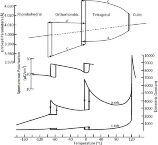
cancel the individual electron spins. Across the Curie temperature, a phase transformation occurs and above the Curie temperature the crystal structure will be centrosymmetric (also called paraelectric phase) while below the Curie temperature it is ferroelectric phase. The ferroelectric phase always has a lower symmetry than the paraelectric phase as shown by the case of BaTiO3 (Figure 1.6). BaTiO3 transforms from the centrosymmetric cubic phase to the low symmetric tetragonal phase at around 120 oC.
Figure 1.6 Temperature-dependent unit cell dimensions, spontaneous polarization, and dielectric constant of BaTiO3.15
17
Among all the ferroelectric materials, PbZrxTi1-xO3 was once extensively studied because of its good thermal stability, strong electrochemical coupling, easy poling and sintering.16, 17 However, more attentions have been drawn to other alternative ferroelectric materials which do not contain the toxic Pb with the increase of environmental consciousness. BaTiO3 is the first perovskite that was discovered to possess ferroelectricity and the first ceramic that was implanted in a piezoelectric transducer.18 BaTiO3 is very stable but its applications are severely limited by the low TC of around 120 oC. Dopants called TC shifters like SrTiO
3, PbTiO3, and CaZrO3 are incorporated to increase or decrease the TC. Stoichiometry is very critical in controlling the ferroelectric response of BaTiO3 because the composition directly determines the unit cell structure and therefore the physical and chemical properties. It was reported that the laser fluence and oxygen partial pressure could both influence the Ba/Ti ratio in the BaTiO3 thin films and therefore the ferroelectric properties (Figure 1.7).19, 20, 21 Another ferroelectric material that is extensively studied is BiFeO3 with a theoretical ferroelectric polarization value of more than 100 C/cm2 and a high TC value of 830 oC. BiFeO
3 will be discussed in more detail in the following section.
18
Figure 1.7 Oxygen pressure dependent (a) Ti/Ba ratio and (b) Pr in BaTiO3 films.21
1.2.2 Magnetism
1.2.2.1 Overview of magnetism
Magnetism is a physical property of a material that responds to an applied magnetic field at atomic or subatomic level. There are several kinds of magnetism depending on the orbital and spin motions of electrons and how the electrons interact with
19
each other.22 With different spin alignments of the electrons, the main magnetic interactions include ferromagnetism, antiferromagnetism, ferrimagnetism, paramagnetism, superparamagnetism, and diamagnetism. For a ferromagnet, spontaneous net magnetization exists even in the absence of an external magnetic field because of the long range and parallel alignment of the atomic magnetic moments. For the ferromagnetic materials, they don’t exhibit net magnetization above the Curie temperature with the atomic moments randomly oriented resulting a paramagnetic phase. For superparamagnetism, it refers to a magnetism existing in small ferromagnetic or ferromagnetic nanoparticles where the magnetization can flip the direction. The net magnetization will be measured to be zero if the time used to measure the magnetization is much longer than the time between two flips (called Neel relaxation time). This small nanoparticle can still be magnetized by applying a magnetic field but the magnetic susceptibility is much larger than that of paramagnets. Antiferromagnetism means that the atomic moments are aligned antiparallel. For ferrimagnetism, the spins are also aligned antiparallel, but the net magnetism is not zero because one subset of dipoles is larger than the other. Diamagnetism is a material property belonging to all materials and can be neglected if the materials show some forms of magnetism such as ferromagnetism and paramagnetism. Diamagnetic materials are usually those nonmagnetic materials including water, wood, most organic compounds, some plastics and many metals such as copper, gold, and bismuth. The magnetic susceptibility for diamagnetic materials is negative. The schematic in Figure 1.8 shows the spin alignment for different magnetism.23
20
Figure 1.8 Schematic diagram showing the spin alignment for different magnetism.23
Several fundamental coupling mechanisms have been developed to explain how indirect exchange which is mediated through nonmagnetic ions like oxygen to give rise the effects in the oxide materials. The three main magnetic coupling model include superexchange, double exchange, and RKKY coupling as shown in Figure 1.9. Superexchange is a magnetic coupling getting its name from the fact that it extends the short-range exchange to long-range interaction which was formally developed in 1950.24 Superexchange can well describe how antiferromagnetism occur in some ionic compounds where 3d and 2p orbitals of transition metals and oxygen/fluorine atoms interact to each other. The superexchange coupling can well describe the antiferromagnetism in LaMnO3. One electron from the 2p orbital of oxygen is donated to the 3d orbital of neighboring Mn and the spins of the two nearest neighboring Mn are antiparallel leading to antiferromagnetism of LaMnO3 as shown by Figure 1.9(a). Double exchange was proposed to describe the magneto-conductive properties of the mixed valence compounds (Sr or Ca doped LaMnO3 on the A site). For the case of La0.7Sr0.3MnO3 containing Mn3+ and Mn4+ the O2- ion has full p-orbitals (Figure 1.9(b)). The electron on the Mn-sites jump back and forth through the oxygen and the electron is thus delocalized over the entire M-O-M group. This model can describe the ferromagnetic alignment and conductive mechanism of La0.7Sr0.3MnO3. RKKY is used to explain the coupling in dilute magnetic
21
semiconductors where the magnetic ions are too far to interact with each other directly (Figure 1.9(c)). This model describes that a local moment can induce a spin polarization which oscillates in sign as a function of distance and this spin information can be carried over relatively long distances.
Figure 1.9 Schematic diagram showing the magnetic couplings in oxides. (a) superexchange, (b) double exchange, and (c) RKKY coupling.8
1.2.2.2 Magnetic ferrites
Several types of magnetic oxides have been investigated both for fundamental study and technological applications. Here two types of magnetic materials will be discussed: ferrites and manganites. Ferrites refers to the Fe-containing oxides including spinels (AFe2O4), garnets (AFe5O12), hexaferrites (AFe12O19), and orthoferrites (RFeO3, R is one or more of the rare-earth elements). Ferrites have been used as transformer cores, microwave magnetic devices, magneto-optic data storage materials, and flux guides and sensors. Among these ferrites, spinel ferrites have been extensively investigated to create high quality thin films to enable better understanding of structure-property relationship. Ferrites have also been widely studied to create vertically aligned nanocomposites for
22
multiferroism.25, 26 In this section, the epitaxial thin films of Fe3O4, NiFe2O4, and CoFe2O4 will be briefly reviewed.
Fe3O4 is an old magnetic material and has been used in the compass for navigation several thousand years ago. Band structure calculations show that the majority of the spin electrons are semiconducting and minority spins metallic.27 Fe3O4 has a high Curie temperature of ~858 K and undergoes a first-order metal-insulator transition from cubic to monoclinic phase with an increase in resistivity and decrease in magnetic moment.28, 29 It is still under debate on the fundamental mechanism of the transition. Epitaxial Fe3O4 thin films have been grown on MgO (001) by various techniques such as pulsed laser deposition with a temperature range of 200 and 500 oC, yield bulk-like properties.30, 31, 32 NiFe2O4 exhibits an insulating state because of the sizeable gap in the majority spins and a smaller one in the minority spins. Epitaxial NiFe2O4 thin films have been fabricated on various substrates including c-plane sapphire and SrTiO3 (001) by pulsed laser deposition.33, 34 Anomalous magnetic behavior including diminished magnetization has been observed for these epitaxial NiFe2O4 thin films.35 During the study of ultrathin films of NiFe2O4 grown on SrTiO3 (001) indicates an anomalous distribution of Fe and Ni cations among the A and B sites and distinctly different magnetic and electronic behaviors including enhanced magnetic moments by 250% and metallic character were observed. For CoFe2O4, the thin film form has quite different properties from its bulk form and the magnetic properties are significantly influenced by the microstructure. Various substrates including MgO (100) and MgAl2O4 (110) have been used to create CoFe2O4 films free of antiphase boundaries which allows the study of the correlation of cation distribution and
23
lattice distortion to the anomalous magnetic behavior.36, 37 As mentioned above, the ferrimagnetic CoFe2O4 has been combined with other oxides to create the vertically aligned nanocomposites for multiferroism recently.25, 26
1.2.2.3 Magnetic manganites
In the past two decades, colossal magnetoresistance (CMR) materials such as doped manganites are especially attractive because of their strong couplings between lattice, charge, spin and orbital degrees of freedom. These manganese-based oxides with perovskite structure shows half-metallic characteristics and CMR response which make these manganites especially intriguing both for fundamental physics study and development of novel electronic devices.
The discovery of CMR effect in La0.67Ca0.33MnO3 thin film has aroused the rejuvenation of research interest in manganite materials. In 1994, Jin et al. reported the thousandfold change in resistivity in the magnetoresistive La0.67Ca0.33MnO3 thin film,38 which is three orders of magnitude larger than that in giant magnetoresistance materials (Figure 1.10). Strain was then believed to play an important role in controlling the physical properties of the manganite thin films. The CMR effect was attributed to the mixed Mn3+ -Mn4+ valence state in La0.67Ca0.33MnO3 thin film. The CMR in La0.67Ca0.33MnO3 thin film requires a large magnetic field which limits its application. Recently, another magnetic transport effect called low-field (< 0.1 T) magnetoresistance has been reported for La0.7Sr0.3MnO3 thin films. Grain boundary was considered to play a predominant role. Chen et al. reported the enhanced low-field magnetoresistance in vertically aligned
24
nanocomposites created from the combination of La0.7Sr0.3MnO3 and other insulating oxides such as ZnO and CeO2.39, 40, 41, 42, 43
Figure 1.10 Magnetoresistance ratio (ΔR/RH) versus temperature curves for the La-Ca-Mn-O films treated under different conditions: curve 1, as deposited; curve 2, annealing at 700 oC in O
2 for 30 min; curve 3, annealing at 900 oC in O2 for 3 hours.38 1.2.3 Multiferroism
1.2.3.1 Overview of multiferroism
Multiferroics refers to a class of materials where at least two primary ferroic orderings coexist in a single material.44, 45, 46 There are four primary ferroic orderings including ferromagnetism, ferroelectricity, ferroelasticity, and ferrotoroidicity.
25
Nowadays, the definition of multiferroics has been expanded and non-primary ferroic orderings are also included such as antiferromagnetism and ferrimagnetism. Ferromagnetism is a phenomenon that a material shows spontaneous magnetization which can be switched by an applied magnetic field. Ferroelectricity is a material property that a material have spontaneous electric polarization and its direction can be reversed by applying an external electric field. Ferroelasticity refers to that a material may have strain due to the externally applied stress. Ferrotoroidicity means a phase transition to spontaneous long-range order of microscopic magnetic toroidal moments but ferrotoroidicity is still under debate because no clear evidence has yet been presented. Among the four primary ferroic orderings, ferroelectricity and ferromagnetism could be coupled to produce the magnetoelectric effect and has received a lot of attention both from the fundamental physics and technological point of view.45, 47 Hereafter, multiferroicity refers specifically to the coexistence of (ferro)magnetism and ferroelectricity as shown by the schematic in Figure 1.11. The magnetoelectric effect was first proposed by Curie in 1894 and confirmed by the work on Cr2O3 in 1960s.48 Taking the advantages of magnetoelectric materials, a wide range of devices with different applications have been proposed, including devices for magnetoelectric data storage and switching, optical diodes, spin-wave generation, amplification, and frequency conversion.
26
Figure 1.11 A schematic showing the relationship between ferroelectricity, magnetism, and multiferroism.49
1.2.3.2 Pathways to multiferroism
Multiferroic materials exhibit great potentials in ferroelectric random access memory, magnetic data storage, multiple state memories, etc. Ni3Bi7O13I is believed to be the earliest multiferroic material which was reported in 1960s.50 With the development of high-quality thin film growth techniques and extensive research on multiferroic materials, different kinds of multiferroics have been discovered or created. From the fundamental mechanism and geometry, the thin film multiferroic materials can be classified into three categories: single-phase epitaxial thin films, horizontal multilayered heterostructures, and vertically aligned heterostructures as shown in Figure 1.12.
27
Figure 1.12 Schematic diagrams showing the three types of multiferroic materials: (a) single-phase epitaxial thin films, (b) horizontal multilayered heterostructures, and (c) vertically aligned heterostructures.44
Horizontal multilayered multiferroic heterostructures is created by atomic level layering to engineer specific magnetic ordering and the compositional ordering leads to polarizations. The multilayered heterostructures include CaTiO3/BaTiO3/SrTiO3, Co-doped TiO2/PZT, Fe/BaTiO3, etc.51, 52, 53 Vertically aligned heterostructures for multiferroism have been fabricated by nanostructured columnar growth of oxide-oxide by careful selection considering lattice matching, immiscibility and different elastic modulus. BaTiO3:CoFe2O4 is one of the typical vertically aligned heterostructures created by the alternating columnar growth of BaTiO3 and CoFe2O4.25, 26, 54 This kind of heterostructure with large interface/volume ratio removes the clamping effect from the substrate and could allow better strain induced couplings. Many other vertically aligned nanostructures have been created for the creation of multiferroics including BiFeO3-CoFe2O4,55 and BaTiO3 -NiFe2O4.56
Compared to the heterostructures mentioned above, single-phase multiferroic thin films are more intriguing with rich physical phenomena behind and could allow the fundamental mechanism study. The single-phase multiferroics can be classified into four
28
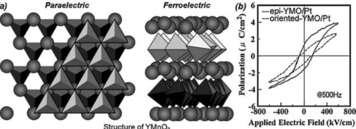
groups based on the mechanism of creating ferroelectricity. The first group is the lone-pair multiferroics which usually have the perovskite structure of the form ABO3, such as BiFeO3,7 BiMnO3,57 and PbVO3.58 The ferroelectricity comes from the stereochemical activity of the lone pair on the A-site cation while the smaller B-site cation provides the magnetism. BiFeO3 and BiMnO3 are two of the most important lone-pair multiferroic materials and will be discussed in detail in the following sections.
The second group is the geometrically driven ferroelectricity which is compatible with the coexistence of magnetism. YMnO359, 60 and BaMF4 (M = Fe, Co, Ni)61, 62 belong to this group. YMnO3 is the earliest hexagonal manganite which was investigated for multiferroism (Figure 1.13). The long range dipole-dipole interactions and oxygen rotations lead to the ferroelectricity and antiferromagnetism. The first epitaxial films of YMnO3 with hexagonal structure was grown by magnetron sputtering on MgO (111) and ZnO (0001)/sapphire (0001).63 Later on, it was found that metastable, non-ferroelectric YMnO3 thin films with orthorhombic structure can be obtained on appropriate substrates such as SrTiO3 (001) and NdGaO3 (101) owing to the epitaxial strain.59 This is the first evidence that strain can be utilized to tune the crystal structure of YMnO3 between hexagonal and orthorhombic phases.