AUTOM
AUTOM
AUTOM
AUTOMATIC PCB DEFECT DETECTION USING
ATIC PCB DEFECT DETECTION USING
ATIC PCB DEFECT DETECTION USING
ATIC PCB DEFECT DETECTION USING
IMAGE SUBTRACTION METHOD
IMAGE SUBTRACTION METHOD
IMAGE SUBTRACTION METHOD
IMAGE SUBTRACTION METHOD
1
Sonal Kaushik , 2Javed Ashraf 1
Research Scholar, 2 M.Tech Assistant Professor
Deptt. of Electronics & Communication Engineering, Al-Falah School of Engineering. & Technology
Abstract
A printed circuit board, or (PCB) is used to mechanically support and electrically connect electronic components using conductive pathways, track or signal traces etched from copper sheets laminated onto anon conductive substrate. The automatic inspection of PCBs serves a purpose which is traditional in computer technology. The purpose is to relieve human inspectors of the tedious and inefficient task of looking for those defects in PCBs which could lead to electric failure. In this project Machine Vision PCB Inspection System is applied at the first step of manufacturing, i.e., the making of bare PCB. We first compare a PCB standard image with a PCB image, using a simple subtraction algorithm that can highlight the main problem-regions. We have also seen the effect of noise in a PCB image that at what level this method is suitable to detect the faulty image. Our focus is to detect defects on printed circuit boards & to see the effect of noise. Typical defects that can be detected are over etchings (opens), under-etchings (shorts), holes etc.
Index terms – Machine vision, PCB defects, Image
Subtraction Algorithm, PCB Inspection
1. INTRODUCTION
Nowadays is necessary to improve the quality of PCB. In manufacturing industry there are defects, Misalignment and orientation error so automated inspection is required. The defects can be analyzed by machine vision using algorithms developed for it. So machine vision provides a measurement technique for regularity and accuracy in the Inspection process. These systems have advantage over human inspection in which subjectivity, fatigue, slowness and high cost is involved. In recent years, the PCB industries require automation due to many reasons. The most important one is the technological advances in PCB’s design and manufacturing. New electronic component fabrication technologies require efficient PCB design and inspection method with compact dimension. The complex and compact design causes difficulties to human inspection process. Another important factor is necessity to reduce the
inspection duration. These factors lead to automation in PCB industry. Nowadays automated systems are preferred in manufacturing industry for higher productivity.
2. METHODS
A. MACHINE VISION
Machine vision (MV) is the technology and methods used to provide imaging-based automatic inspection and analysis for such applications as automatic inspection, process control, and robot guidance in industry. Machine vision is concerned with the theory behind artificial systems that extract information from images and sequence of images. The image data can take many forms, such as video sequences, views from multiple cameras, or multi-dimensional data from a medical scanner.
B. BARE PCB DEFECTS
There are some defects commonly found on PCB. Conductor breaking and short-circuit are characterized as fatal defects.
Pinhole, breakout, Over etch, and under etch are characterized as potential defects. Fatal defects are those in which the PCB does not attend the objective they are designed for, and potential defects are those compromising the PCB during their utilization.
During etching process, the anomalies occurring on bare PCB could be largely classified in two categories: the one is excess of Copper and the other one is missing copper. The incomplete etching process leaves unwanted conductive materials and forms defects like short, extra hole, protrusion, island, and small space. The excessive etching makes open, pin hole, nick (mouse bite), and thin pattern. In addition to the defects mentioned above, some other defects may exist on bare PCB, for example, missing holes
(due to tool break), scratch (due to handling mistake), and cracks.
Defect Causes
Typical causes of failure include:
• Board delamination
• Component misalignment
• Broken metal lines
• Cold-solder joints and poor die bonding
• Surface contamination by metal and ionic residues
FIG.1 TEMPLATE PCB
FIG.2 DEFECTED PCB
3. TECHNOLOGY DESCRIPTION
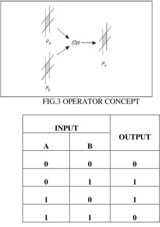
An arithmetic or logic operation between images is a pixel-by-pixel transformation. It produces an image in which each pixel derives its value from the value of pixels with the same coordinates in other images.
If A and B are the images with a resolution XY, and Op is
the operator, then the image N resulting from the combination of A and B through the operator Op (fig.2) is such that each pixel P of the resulting image N is assigned
the value pn = (pa)(Op)(pb) ; where pa is the value of pixel
P in image A, and pb is the value of pixel P in image B.
FIG.3 OPERATOR CONCEPT
INPUT OUTPUT A B 0 0 0 0 1 1 1 0 1 1 1 0
TRUTH TABLE OF XOR OPERATOR
4. PROCESS FLOWCHART
Fig. 4 shows a process flowchart explaining how we will implement image subtraction method and how the results will be analysed.
A. THRESHOLDING
Single Thresholding: A gray scale image is turned into a binary image by first choosing a gray level T in the original image, and then turning every pixel black or white according to whether its gray value is greater than or less than T.
• A pixel becomes white if its gray level is > T
• A pixel becomes black if its gray level is <= T
Double Thresholding: Here we choose two values T1 and T2 and apply a thresholding operation as:
• A pixel becomes white if its gray level between T1 and T2
• A pixel becomes black if its gray level is otherwise
B. SPATIAL FILTERING
• Move a “mask”: a rectangle (usually with sides of odd length) or other shape over the given
Image.
• A new image whose pixels have gray values calculated from the gray values under the mask.
• The combination of mask and function is called filter. • Linear function of all the gray values in the mask, then the filter is called a linear filter.
• Spatial filtering requires 3 steps:
1. Position the mask over the current pixel,
2. Form all products of filter elements with the corresponding elements of the neighborhood.
3. Add up all the products.
• This must be repeated for every pixel in the image. • filter2(filter,image,shape)
C. FREQUENCIES: Low and High Pass Filters
• Frequencies are the amount by which grey values change with distance.
• High frequency components are characterized by large changes in grey values over small distances; (edges and noise)
• Low frequency components are parts characterized by little change in the gray values. (Backgrounds, skin textures)
• High pass filter: if it “passes over” the high frequency components, and reduces or eliminates low frequency components.
• Low pass filter: if it “passes over” the low frequency components, and reduces or eliminates high frequency components.
D. NOISE
Noise is any degradation in the image signal, caused by external disturbance.
• Salt and pepper noise: It is caused by sharp, sudden disturbances in the image signal; it is randomly scattered white or black (or both) pixels. It can be modeled by random values added to an image
• Gaussian noise: is an idealized form of white noise, which is caused by random fluctuations in the signal. • Speckle noise: It is a major problem in some radar applications. It can be modeled by random values multiplied by pixel values.
5. ALGORITHM STEPS
Most existing approaches are based on the following steps: 1. Noisy: RGB image, defected PCB, which is to be analyzed and other is Template: RGB image, Perfect PCB with no defects.
2. Conversion of both template PCB & defected PCB is done from RGB to Binary image.
3. The correlation of both the binary images i.e template & defected PCB image provides an resultant image which is the
difference of both the images.
4. The difference of both images is an image, which will be nothing but highlighting the noise in the PCB.
5. With the application of filters noise can be removed up to an extent so that defect can be easily pointed.
6. RESULTS AND DISCUSSION
Based on the algorithms shown above, these algorithms need two images, namely template image and defective image. In this paper, these algorithms use Figure 1 as template image and Figure 2 as defective image. At first, both images are subjected to image subtraction operation to produce an resultant image. Then, XOR operator is applied to template image and the defective image separately to produce A1 image, respectively. In this we have done testing for three different defective PCBs & then by increasing the noise level for each image seen that how much this method is capable to detect a faulty PCB & then graph is plotted b/w Noise level Vs Detection ratio. From there, the algorithms continue to produce the results. The results shown will be based on these images.
A Testing of faulty PCB 1
PCB 1 fails to detect at noise level 0.02
S.No Noise level Succ/Fail
1 0.00001 S 2 0.00005 S 3 0.0001 S 4 0.0005 S 5 0.001 S 6 0.005 S 7 0.01 S 8 0.02 F 9 0.05 F 10 0.1 F TABLE 5.1 GRAPH 5.1 B Testing of faulty PCB 2
PCB 2 fails to detect at noise level 0.03
S.No Noise level Succ/Fail
1 0.00001 S 2 0.00005 S 3 0.0001 S 4 0.0005 S 5 0.001 S 6 0.005 S 7 0.01 S 8 0.02 S 9 0.03 F 10 0.05 F TABLE 5.2 GRAPH 5.2 C Testing of faulty PCB 3
PCB 3 fails to detect at noise level 0.01
S.No Noise level Succ/Fail
1 0.00001 S 2 0.00005 S 3 0.0001 S 4 0.0005 S 5 0.001 S 6 0.005 S 7 0.01 F 8 0.02 F 9 0.05 F 10 0.1 F TABLE 5.3
GRAPH 5.3
6. CONCLUSION
PCB quality testing is very important from the point of view of sales and ultimately success of the product. Our simulated work in this research gave rise to lots of useful insights.
Especially, it is very clear now that using machine vision many of the defects on the PCB can be detected with good accuracy. Also we concluded that effect of noise can also be one of the major factors in detecting defects. The effect of noise can be seen in the graphs. The source of such noise could be noise in the CCD's signal itself or it could be some noise between CCD and original object.
We see that our simulation works very well for different types of template and not just for a single type of template. With power of tools such as MATLAB, we were able to capture useful information, and process the same to detect the defects.
REFERENCES
[1] M. Mogant and F. Ereal, “A subpattern level inspection system for printed circuit board,” Computer Vision and
Image Understanding, 70, pp. 51-62, 1998.
[2] C. -S. Lin and L. W. Lue, “Image system for fast positioning and accuracy inspection of ball grid array boards,” Microelectronics and Reliability, 41, pp. 119-128, 2001.
[3] J. Beamish, “Printed circuit board
fabricationprocedures,”http://www.mansys.herts.ac.uk/john/
pcbstuff/PCBFabrication.html, University of
Hertfordshire, UK.
[4] K. V. Ramana and B. Ramamoorthy, “Statistical methods to compare the texture features of machined surfaces,” Pattern Recognition, 29, pp. 1447-1459, 1996. 9. S. S. Liu and M. E. Jernigan, “Texture analysis and discrimination in additive noise,” Computer Vision,
Graphics and Image Processing, 49, pp. 52-67, 1990.
[5] R. Muzzolini, Y. -H. Yang and R. Pierson, “Texture characterization using robust statistics,” Pattern
Recognition, 27, pp. 119-134, 1994.11. C. E. Shannon and
W. Weaver, The Mathematical Theory of Communication, University of Illinois Press, Urbana, IL, 1949.
[6] A. Sprague, M. Donahue, and S. Rokhlin, “Amethod for automatic inspection of printed circuit boards,” Graphical Model and Image Processing,vol. 54, no. 3, pp. 401–415, 1991.
[7] Y. Hara, N. Akiyama, and K. Karasaki, “Automatic inspection system for printed circuit
boards,” IEEE Transactions on Pattern Analysisand Machine Intelligence, vol. 5, no. 6, pp. 623–
630, 1983.
[8] F. J. Langley, “Imaging systems for PCB inspection ,”Circuit Manufacturing, vol. 25, no. 1, pp. 50–54, 1985. [9] S. Mukai, “PCB continuous line system proceeds from manufacturing to inspection,” Electronic Engineering, vol. 39, no. 305, pp. 34–39,1992.
[10] M. Moganti, F. Ercal, C. H. Dagli, andS. Tsunekawa, “Automatic PCB inspection algorithms:
A survey,” Computer Vision and ImageUnderstanding, vol. 63, no. 2, pp. 287–313,1996.
[11] Der-Baau Perng, Chuan-Pei Liu, Yen-Chung Chen, and Cheng-Chuan Chou, Advanced Smd Pcb Vision
Inspection Machine Development Department of Industrial
Engineering and Management National Chiao-Tung University, 15th IPPR Conference on Computer Vision, Graphics and Image Processing, 2002
[12] Yi L et al "Machine Vision Algorithms Using
Interactive LearningFor VFD Inspection," Journal of
Applied Intelligence, 2000
[13] Y. Sun, C Tsai. “A New Model-Based Approach for
Industrial Visual Inspection”, Pattern Recognition, Vol. 25,
[14] W. Wu, M. Wang and C. Liu, Automated inspection of
printed circuit boards through machine vision, Computers
in Industry 28, pp103-111, 1996.
[15] Moganti, M., Ercal, F., Dagli, C. H. and Shou, Tsunekawa,“Automatic PCB Inspection Algorithms: A
Survey”, Computer Vision and Image Understanding, Vol.
63, No.2, (1996), pp. 287-313.
[16] Ajay pal singh chauhan, sharat Chandra bhardwaj for automatic inspection of printed circuit boards,” detection of bare pcb defectsby image subtraction method using