160
Implementation Of Network On-Chip Using GALS
Scheme
B. Nagaveni, G. Sai Thirumal, M. Rami Reddy
Abstract: The Network-on-Chip (NOC) concept has recently become a widely discussed technique for handling the large on -chip communication requirements of complex System-on- Chip (SOC) designs. A traditional bus-based interconnection scheme does not scale well to very large SOCs because many Intellectual Property (IP) blocks must contend with each other to communicate over the shared bus. In contrast, an on-chip network uses the packet-switching paradigm to route information between IP blocks and it can be scaled up to achieve a very lar ge total aggregate bandwidth within the chip. The issues of applying the Code-Division Multiple Access (CDMA) technique to an on-chip packet switched communication network are discussed in this paper. A packet switched Network-on-Chip (NOC) that applies the CDMA technique is realized in Register-Transfer Level (RTL) using VHDL. The realized CDMA NOC supports the Globally-Asynchronous Locally-Synchronous (GALS) communication scheme by applying both synchronous and asynchronous designs. In a packet switched NOC, which applies a point-to-point connection scheme, e.g., a ring topology NOC, data transfer latency varies largely if the packets are transferred to different destinations or to the same destination through different routes in the network. The CDMA NOC can eliminate the data transfer latency variations by sharing the data communication media among multiple users concurrently. A six-node GALS CDMA on-chip network is modeled and simulated. The characteristics of the CDMA NOC are examined by comparing them with the characteristics of an on-chip bidirectional ring topology network. The simulation results reveal that the data transfer latency in the CDMA NOC is a constant value for a certain length of packet and is equivalent to the best case data transfer lat ency in the bidirectional ring network when data path width is set to 32 bits.
Index Terms: CDMA (Code Division Multiple Access), IC (Integrated Circuit Design), NoC (Network on-Chip), GALS (Globally Asynchronous Locally Synchronous), RTL (Register Transfer Level), VHDL (VHSIC Hardware Descriptive Language), FPGA (Field Programmable Gate Array).
————————————————————
1
I
NTRODUCTIONOMMUNICATIONS play a fundamental and crucial role for the development of human society in every aspect because better communications facilitate better understanding and cooperation between individuals. As in electronics field, believe be that the same truth also applies to on-chip systems, which means that the quality of communication in an on-chip system prominently affects system performance. As the complexity of an on-chip system keeps growing, the communication among functional hosts in the system becomes a non-trivial issue to deal with. Currently, silicon chips which contain thousands of millions of transistors with 45nm feature size are already available on market, e.g. Intel Pentium processor. According to the report from International Technology Roadmap for Semiconductors (ITRS) in 2007, a single semi-conductor chip will contain multi-billion transistors with feature sizes around 22nm and clock frequencies around 35GHz by the year of 2016. This growing manufacture capacity and the highly demanding applications continuously drive the complexity of a System-on- Chip (SOC) to a higher degree in terms of number of system components and functionalities. For example, Cell Broadband Engine Architecture (CBEA) jointly developed by IBM, Sony, and Toshiba, also referred as Cell processor, contains altogether 9 processing units in one chip. Furthermore, Tierra, a MIT spin-off company, released a 64-core processor called TILE 64 in 2007. As the number of system components becomes larger, current widely applied bus structures for data transfers in an on-chip system, e.g. Core Connect, expose Several disadvantages as addressed Two main disadvantages are bus arbitration bottleneck and bandwidth limitation. The arbitration bottleneck means that the arbitration delay will grow if the number of bus hosts increases. The bandwidth limitation refers to the fact that the data transfer bandwidth of a bus structure is shared by all hosts attached to it in a time division manner. Hence, more hosts incur a lower share of bandwidth for each one Another challenge that an on-chip system faces is the heterogeneous characteristics of system components. The components in a SOC may include processors for
computation tasks, functional blocks for accelerating certain tasks, and the modules for communicating with the peripherals of system. The different functions among different system components naturally cause them to work in different clock rates for optimal performance. Hence, coordination and communications among those components become challenging tasks. At the same time, the issues of wire delay, on-chip noise, process variance, and power consumption in the realm of Deep Sub-Micron (DSM) technologies also become challenging for chip design. Altogether, these challenges have brought more and more concerns on the on-chip communication issue of a SOC design. In order to overcome the disadvantages of bus structures, the concept of Network-on-Chip (NOC) has been proposed as a solution at the beginning of 2000s, The idea of NOC is to separate the concerns of communication from computation by building on-chip communication structure with concepts adopted from computer networks. Each component of a SOC is viewed as a node of the on-chip communication network. System components communicate with each other through the on-chip network. For the challenges of multiple clock domains and DSM technology effect, Globally-Asynchronous Locally-Synchronous (GALS) scheme has been proposed as a solution. The idea of a GALS system is to partition a system into separate clock domains which run at different clock rates, and the separated domains communicate with each other in an asynchronous manner.
2
N
ETWORKONCHIPnow a days and believed to be valid until reaching the size of atoms. Therefore, driven by the growing manufacture capacity and the growing requirement of applications, the complexity of an on-chip system is continuously growing in terms of number of transistors and functionalities. Intel‘s ‗Core 2 Duo‘ processor fabricated with 65nm technology process contains 291 million transistors. When the on-chip system becomes complicated, the system design methodology called orthogonalization of concerns can be applied to deal with the complexity. The communication issue is very crucial for an on-chip system to perform its tasks efficiently. Therefore, in the context of SOC design, one way of applying the methodology of concerns orthogonalization is to separate the concerns of communication from computation to enable more efficient exploration of optimal solutions on each subject. However, as addressed in, bus structures have several disadvantages by the comparison of on-chip networks. The main disadvantages, bus arbitration bottleneck and bandwidth limitation are caused by the centralized and time division manner of sharing a communication channel among all the hosts of a bus. The trend of future on-chip systems is that a large number of processing units will be integrated into one system. Therefore, if a bus structure is applied in the future on-chip systems which contain a large number of components, it will suffer from the problems of arbitration delay, bandwidth limitation, and poor scalability. Hence, developing a dedicated on-chip network is the most promising solution for future on-chip communication.
3
DIGITAL
ENCODING
&
DECODING
SCHEMEFig. 1. Digital CDMA encoding scheme
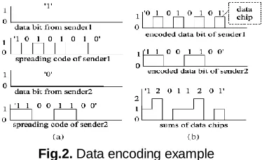
Several on-chip bus schemes that apply the CDMA technique have been presented . Those schemes are implemented by analog circuits, namely, the encoded data are represented by the continuous voltage or capacitance value of the circuits.Therefore, the data transfers in the analog bus are challenged by the coupling noise, clock skew, and the variations of capacitance and resistance caused by circuit implementation. In order to avoid the challenges faced by the analog circuit implementation, digital encoding and decoding schemes developed for the CDMA NoC are illustrated in Figs. 1 and 3, respectively. In the encoding scheme illustrated in Fig. 1, data from different senders fed into the encoder bit by bit. Each data bit will be spread into S bits by XOR logic operations with a unique S-bit spreading code as illustrated in Fig. 1. Each bit of the S-bit encoded data generated by XOR operations is called a data chip. Then, the data chips which come from different senders are added together arithmetically
according to their bit positions in the S-bit sequences. Namely, all the first data chips from different senders are added together and all the second data chips from different senders are added together, and so on. Therefore, after the add operations, we will get S sum values of S-bit encoded data. Binary equivalents of the S sum values are transferred to the receiving end. An example of encoding two data bits from two senders is illustrated in Fig. 2 in order to illustrate the proposed encoding scheme in more detail.
Fig.2. Data encoding example
162 FIG.3.DIGITAL CDMA DECODING SCHEME
4
SPREADING
CODE
PROTOCOL
In a CDMA network, if multiple users use the same spreading code to encode their data packets for transmission simultaneously, the data to be transferred will interfere with each other because of the loss of orthogonal property among the spreading codes. This situation is called spreading code conflict, which should be avoided. Spreading code protocol is a policy used to decide how to assign and use the spreading codes in a CDMA network in order to eliminate or reduce the possible spreading code conflicts during the communication processes. Several spreading code protocols have been presented for CDMA packet radio network and will be shortly introduced in the following six paragraphs.
1) Common Code Protocol (C protocol): All users in
the network use the same spreading code to encode their data packets to be transferred.
2) Receiver-Based Protocol (R protocol): Each user in
the network is assigned a unique spreading code used by the other users who want to send data to that user.
3) Transmitter-Based Protocol (T protocol): The
unique spreading code allocated to each user is used by the user himself to transfer data to others.
4) Common-Transmitter-Based Protocol (C-T
protocol): The destination address portion of a data
packet is encoded using C protocol, whereas, the data portion of a packet is encoded using T protocol.
5) Receiver-Transmitter-Based Protocol (R-T
protocol): It is the same as the C-T protocol except
that the destination address portion of a data packet is encoded using R protocol.
6) Transmitter-Receiver-Based Protocol (T-R
protocol): Two unique spreading codes are assigned
to each user in the network, and then a user will generate a new spreading code from the assigned two unique codes for its data encoding.
5
G
ALSSCHEMENOCSTRUCTUREUSINGCDMAApplying the GALS scheme to the CDMA NoC means that the communications between each functional host and its network node use local clock frequency, while the communications between network nodes through the CDMA network are asynchronous. In order to support the GALS scheme, both synchronous and asynchronous circuits are applied in the design. The proposed CDMA NoC is a packet switched network that consists of ―Network Node,‖ ―CDMA Transmitter,‖ and ―Network Arbiter‖ blocks as illustrated in Fig. 4.
Fig.4.Proposed GALS Scheme NOC Structure Using CDMA
The functional IP blocks (functional hosts) are connected to the CDMA NoC through individual ―Network Node‖ blocks. The CDMA communications in the network are performed by ―CDMA Transmitter‖ and ―Network Arbiter‖ blocks. Because the different functional hosts may work at different clock frequencies as illustrated in Fig. 4, coordinating the data transfers among different clock domains would be a problem. A globally-asynchronous locally-synchronous (GALS) scheme has been proposed as a solution for this problem. The three types of components in the CDMA NoC will be presented in the following three subsections.
A. Network node. B. Network arbiter. C. CDMA Transmitter
Fig.5.Block diagram of the network node in CDMA NOC
5.1 NETWORK NODE
The block diagram of the ―Network Node‖ in the CDMA NoC is illustrated in Fig. 5, where the arrows represent the flows of data packets. In Fig. 5, the ―Network IF‖ block, which belongs to the functional host, is an interface block for connecting a functional host with a ―Network Node‖ through VCI or OCP interface standard . GALS scheme is realized in ―Network Node‖ block by using synchronous design in the ―Node IF‖ subblock and using asynchronous design in the other subblocks. The function of the subblocks in a ―Network Node‖ will be described in the following four paragraphs.
1) Node IF: This block is used to receive data from the
―Network IF‖ block of a functional host through the applied VCI or OCP standard. Then it will assemble the received data into packet format and send the packet to ―Tx Packet Buffer,‖ or disassemble the received packet from ―Rx Packet Buffer‖ and send the extracted data to the functional host.
2) Tx/Rx Packet Buffer: These two blocks are buffers that
presented in . ―Tx Packet Buffer‖ is used to store the data packets from ―Node IF‖ block, and then deliver the packets to ―Packet Sender‖ block. The ―Rx Packet Buffer‖ stores and delivers the received packets from ―Packet Receiver‖ to ―Node IF.‖
3) Packet Sender: If ―Tx Packet Buffer‖ is not empty, ―Packet
Sender‖ will fetch a data packet from the buffer by an asynchronous handshake protocol. Then it will extract the destination information from the fetched packet and send the destination address to ―Network Arbiter.‖ After ―Packet Sender‖ gets the grant signal from the arbiter, it will start to send the data packet to ―CDMA Transmitter.‖
4) Packet Receiver: After system reset, this block will wait for
the sender information from ―Network Arbiter‖ to select the proper spreading code for decoding. After the spreading code for decoding is ready, the receiver will send an acknowledge signal back to ―Network Arbiter‖ and wait to receive and decode the data from ―CDMA Transmitter,‖ and then send the decoded data to ―Rx Packet Buffer‖ in packet format.
5.2 Network Arbiter
―Network Arbiter‖ block is the core component to implement the A-T spreading code protocol. By applying A-T spreading code protocol, every sender node cannot start to send data packets to ―CDMA Transmitter‖ until it gets the grant signal from ―Network Arbiter.‖ ―Network Arbiter‖ takes charge of informing the requested receiver node to prepare the proper spreading code for decoding and sending a grant signal back to the sender node. In the case that there are more than one sender nodes requesting to send data to the same receiver node simultaneously or at different times, the arbiter will apply a ―round-robin‖ arbitration scheme or the ―come first-served‖ principle, respectively, to guarantee that there is only one sender sending data to one specific receiver at a time. However, if different sender nodes request to send data to different receiver nodes, these requests would not block each other and will be handled in parallel in the ―Network Arbiter.‖ The ―Network Arbiter‖ in the CDMA NoC is different from the arbiter used in a conventional bus. The reason is that the ―Network Arbiter‖ here is only used to set up spreading codes for receiving and it handles the requests in parallel in the time domain. However, a conventional bus arbiter is used to allocate the usage of the common communication media among the users in the time-division manner.
5.3 CDMA Transmitter
The ―CDMA Transmitter‖ block takes care of receiving data packets from network nodes and encoding the data to be transferred with the corresponding unique spreading code of the sender node. Although this block is realized using asynchronous circuits, it applies a bit-synchronous transfer scheme. It means that the data from different nodes will be encoded and transmitted synchronously in terms of data bits rather than any clock signals. the principle of the referred bit-synchronous transfer scheme is illustrated by a situation that network nodes ―A‖ and ―B‖ send data packets to ―CDMA Transmitter‖ simultaneously and node ―C‖ sends a data packet later than ―A‖ and ―B.‖ In this situation, the data packet from node ―A‖ will be encoded and transmitted together with the data packet from node ―B‖ synchronously in terms of each data bit. When the data packet from node ―C‖ arrives at a later
time point, the transmitter will handle the data bit of ―Packet C‖ together with the data bits of packet ―A‖ and ―B‖ at the next start point of the time slot for bit encoding and transmitting processes. The dot-line frame at the head of the ―Packet C‖ is used to illustrate the waiting duration if the ―Packet C‖ arrived in the middle of the time slot for handling the previous data bit. The time slot for handling a data bit is formed by a four-phase handshake process. The bit-synchronous transfer scheme can avoid the interferences caused by the phase offsets among the orthogonal spreading codes if the data bits from different nodes are encoded and transmitted asynchronously with each other. Because the nodes in the network can request data transfer randomly and independently of each other, ―CDMA Transmitter‖ applies the ―first come, first served‖ mechanism to ensure that the data encoding and transmission are performed as soon as there is data transfer request.
6
SIMULATION
Simulation is to verify design. Thus it is first step after design and coding is done. it is totally software activity where verify the design using simulators like Xilinx. This step is also called as functional simulations. In other way simulation is nothing but whatever expected logical functionality checking in hardware world, without considering the actual timing issues i.e.net delay and circuit delays. Each module is coded in verilog and simulated. The simulation result and the net list simulation are verified for each module. to simulate the design, Xilinx simulator is used.
Fig.6(a) simulation diagram of CDMA-NOC
Fig.6(b).simulation diagram of CDMA-NOC
7
S
IMULATIONN
ETWORKS
ETUP164 through ―CDMA Transmitter‖ and ―Network Arbiter‖ blocks. The
spreading codes used in the network are six 8-bit Walsh codes. The basic data unit transferred in the network is data packets composed by one header cell and several data cells. The number of data cells in a packet varies from one to three, while the width of each packet cell is fixed at 32 bits. The ―functional host‖ blocks and their ―Network IF‖ blocks are not realized with any real IP blocks; they are simulated by adding stimulus signals on each ―Network Node‖ block according to the BVCI standard. A four-phase dual-rail handshake protocol is applied in the CDMA network to transfer data between network nodes. The PTP network has the same mentioned network configurations as the CDMA network except that the network nodes in the PTP network are connected with each other through bidirectional ring topology. Therefore, the characteristics of the CDMA NoC can be examined more clearly by comparing the two networks in different aspects in the following four subsections
Fig.7. Six-node CDMA NoC simulation network
8 Comparison of Data Transfer Latencies
The CDMA network illustrated in Fig. 7 and the PTP NoC illustrated in Fig. 9 are both synthesized using the same 0.18- m technology library. Gate-level simulations are performed on both simulation networks. The data transactions performed during the simulations. Each data transaction consists of one request packet from an initiator host to a target host and one corresponding response packet from the target host to the initiator host. Because the GALS scheme is applied both in the CDMA network and the PTP network, the data transfer latency in the two simulation networks can be separated into two parts, synchronous transfer latency (STL) and asynchronous transfer latency (ATL). The STL refers to the data transfer latency between a functional host and the network node attached to it. STL depends on the local clock and the type of interface. The constant values are caused by the handshakes in the asynchronous domain. They are independent of the local clock rate but belong to the synchronous transfer processes. Therefore, they are counted as a part of STL. We can see that an initiator type of network node takes more clock cycles for local data transfers. The reason is that the initiator node needs to store or read the header cell to or from a buffer. Since the same ―Node IF‖ block design is applied in both simulation networks, the STL of the PTP network has the same value. The ATL refers to the data transfer latency of transferring data packets from one network node to the other node through a NoC structure using asynchronous handshake protocols. The ATL values in the PTP and CDMA networks consist of different portions which will be discussed separately
in the following subsections.
1) ATL in the CDMA NoC: The ATL of the CDMA network
consists of three portions: packet loading latency (PLL), packet transfer latency (PTL), and packet storing latency (PSL). The concept of those ATL portions with an example where ―Network Node 0‖ sends one data packet to ―Network Node 2.‖ The black arrows represent the packet transfer direction. The different portions of ATL are marked by grey arrows and explained in the following three paragraphs.
FIG.10. ATL PORTIONS OF THE CDMA NOC
a) PLL: This is the time used by the ―Packet Sender‖ block to fetch a data packet from ―Tx Packet Buffer‖ and prepare to send the packet to ―CDMA Transmitter.‖
b) PTL: This latency refers to the time used to transfer one data packet from the ―Packet Sender‖ of the sender node to the ―Packet Receiver‖ of the receiver node through the ―CDMA Transmitter‖ and ―Network Arbiter‖ blocks using a handshake protocol.
c) PSL: After the receiver node receives a data packet, it will spend a certain amount of time to store the received data packet into ―Rx Packet Buffer.‖ This time duration is measured as PSL.
The ATL value of the CDMA NoC can be calculated by directly adding the three portions under the same configuration.
2) ATL in the PTP NoC: The concept of the ATL portions of the PTP NoC is illustrated with an example that ―Network Node 0‖ sends one packet to ―Network Node 2‖ via., ―Network Node 1.‖ The black and grey arrows represent the same meanings as the arrows . The meaning of ATL portions will be explained briefly in the following four paragraphs.
b) PTL: This latency refers to the time used to transfer one data packet from the ―Packet Sender‖
(1)of a network node to the ―Packet Receiver‖ of an adjacent node using a handshake protocol.
c) PBL: After a network node receives a packet from another node, it will check its destination address. If it is a ―bypass packet,‖ it will be delivered into ―Tx Packet Buffer.‖ The time spent on this process is called PBL.
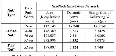
Table 1 Comparison of area and power costs
9 APPLICATIONS
1. Internet applications.2. Mother board communications. 3. ON-Chip communications.
10
C
ONCLUSIONAn on-chip packet switched communication network that applies the CDMA technique and supports the GALS communication scheme was presented. The presented CDMA NoC uses an asynchronous scheme to perform the global data transfers between network nodes, and uses synchronous scheme to deal with the local data transfers between a functional host and the network node attached to it. A CDMA encoding and decoding scheme which suits digital-circuit implementation was presented. The main advantage of the presented CDMA NoC is that it can perform data transfer concurrently by ap- plying CDMA technique in the network. Therefore, the large data transfer latency variance caused by the packet routing in a PTP NoC is eliminated in the CDMA NoC. The constant data transfer latency in the CDMA NoC is helpful for providing guaranteed communication services to an on-chip system. Another advantage of the CDMA NoC is that it can perform multicast data transfers easily by utilizing the multiple access feature of CDMA technique. Both the asynchronous and synchronous circuits of the CDMA NoC with different data path widths are realized in RTL using VHDL in order to suit the conventional synchronous design flow and tools. Two six-node on-chip networks were constructed to compare the CDMA NoC with a PTP NoC. One network applies the CDMA NoC, while the other applies a bidirectional ring PTP NoC. The two networks were simulated and compared against each other. The simulation results reveal that when the data path width of the two simulation networks is set to 32 bits, the asynchronous transfer latency in the CDMA NoC is equivalent to the best case data transfer latency in the PTP NoC. The best case data transfer in the PTP NoC means that packets are transferred between two adjacent nodes. It indicates that the data transfers between any network nodes in the CDMA NoC can be performed as quickly as transferring the same data packets between two adjacent nodes in the PTP NoC . With a 16-bit data path width, the data transfer latency of the CDMA NoC is close to the best case transfer latency in the PTP NoC while the area and dynamic power costs remain similar. If the area and power costs have higher priority, the 8-bit CDMA NoC can be applied because its area is 16.2% smaller than the PTP NoC while its energy cost of transferring 32 bits is 21.0% smaller than the cost in the PTP NoC.
R
EFERENCES[1]. D. Wiklund and D. Liu, "SoCBUS: Switched network on chip for hard real time systems," in Proc. Int. Parallel Distrib. Process. Symp. (IPDPS), 2003, p. 8.
[2]. D. Sigüenza-Tortosa, T. Ahonen, and J. Nurmi, "Issues in the develop- ment of a practical NoC: The proteo concept," Integr., VLSI J., vol. 38,no. 1, pp. 95-105, 2004.
[3]. A. J. Viterbi, CDMA: Principles of Spread Spectrum
Communica- tions. Reading, MA: Addison-Wesley,
1995.
[4]. R. Yoshimura, T. B. Keat, T. Ogawa, S. Hatanaka, T. Matsuoka, and K. Taniguchi, "DS-CDMA wired bus with simple interconnection topology for parallel processing system LSIs," in Dig. Tech. Papers IEEE Int. Solid-State Circuits Conf., 2000, pp. 370-371.
[5]. M. Takahashi, T. B. Keat, H. Iwamura, T. Matsuoka, and K. Taniguchi, "A study of robustness and coupling-noise immunity on simultaneous data transfer CDMA bus interface," in Proc. IEEE Int. Symp.CircuitsSyst., 2002, pp. 611-614.
[6]. R. H. Bell, Jr., K. Y. Chang, L. John, and E. E. Swartzlander, Jr.,"CDMA as a multiprocessor interconnect strategy," in Con]. Record 35th Asilomar
Con]. Signals, Syst. Comput., 2001, pp. 1246-1250.
[7]. E. S. Sousa and J. A. Silvester, "Spreading code protocols for distributed spread-spectrum packet radio networks," IEEE Trans. Commun., vol. 36, no. 3, pp. 272-281, Mar. 1988.
[8]. D. D. Lin and T. J. Lim, "Subspace-based active user identification for a collision-free slotted ad hoc network," IEEE Trans. Commun., vol. 52, no. 4, pp. 612-621, Apr. 2004.
[9]. [9] D. M. Chapiro, "Globally-asynchronous locally-synchronous sys- tems," Ph.D. dissertation, Dept. Comput. Sci., Stanford University, Stanford, CA, 1984.
[10]. OCP-International Partnership. Beaverton, OR, "Open core protocol specification," 2001. [Online]. Available: http://www.ocpip.org/