NEW APPLICATIONS OF EXCIMER LAMPS
TO THE LOW TEMPERATURE
PHOTO-DEPOSITION OF THIN FILMS
A thesis submitted to the University of London
for the degree of Doctor of Philosophy
PHILIPPE BERGONZO
ProQuest Number: 10055371
All rights reserved
INFORMATION TO ALL USERS
The quality of this reproduction is dependent upon the quality of the copy submitted.
In the unlikely event that the author did not send a complete manuscript
and there are missing pages, th ese will be noted. Also, if material had to be removed, a note will indicate the deletion.
uest.
ProQuest 10055371
Published by ProQuest LLC(2016). Copyright of the Dissertation is held by the Author.
All rights reserved.
This work is protected against unauthorized copying under Title 17, United States Code. Microform Edition © ProQuest LLC.
ProQuest LLC
789 East Eisenhower Parkway P.O. Box 1346
Abstract
Over the last decade, the requirement for low temperature processing in the semiconductor industry has become apparent due to the continued reduction in device geometry and the emergence of temperature sensitive materials. Of the low temperature techniques available, photo-enhanced processing of materials is very promising since the growing films are not subject to damaging ionic bombardment which is present in plasma assisted systems. Here is presented the development of a flexible large area, low temperature photo enhanced chemical vapour deposition reactor (photo-CVD) for apphcations to low temperature thin films processing.
The development of novel excimer lamps has opened up the field of direct photo- CVD. Such lamps are a cheap and intense source of visible, UV and vacuum ultraviolet radiation (YUV: below 200nm), The major breakthrough with the development of these lamps is that they offer a large number of wavelengths that can be used for selective photo-CVD. The fabrication and characterisation of those light sources were conducted, and various devices generating up to a few watts are presented. Applications of the available radiation are also presented such as for the direct VUV enhanced generation of ozone and various metal-organic depositions (MOD).
For the first time, the 172nm radiation of a xenon excimer lamp has been used to deposit silicon dioxide (Si0 2 ), silicon nitride (SigN^), and silicon oxynitride films
from the photo-CVD of gas mixtures of silane with nitrous oxide and anunonia, and at temperatures as low as 300°C. Fast deposition (up to 500Â/min) of Si0 2 was also
achieved by irradiating silane and oxygen gas mixtures. Investigations into the deposition photochemistry are reported, together with the characterisation of the deposited material properties. Good Si0 2 and SigN^ film quality was obtained, as
well as a very good control of the stoichiometry in the case of silicon oxynitride film deposition, therefore providing interesting perspectives for electronic and optical applications.
Acknowledgements
The completion of this project would not have been possible without the help and assistance from a number of people, all of whom contributed in their own special way, and rightly deserve their mention here.
I am grateful to all the persons who allowed me to use their equipment, such as Prof. M. Green for the ellip some try measurements. Dr. S. Best and Miss E. Lloyd for the FTIR analyses, and Dr. S.J.B. Corrigan who lent me a vacuum ultraviolet monochromator without expecting it back. I would also like to acknowledge Dr. M. Dubois for the SIMS analysis, and Dr. V. Craciun and his Romanian compatriots who did the XPS measurements.
I am deeply indebted to Dr Frank Beech and Dr. Glenn C. Tyrrell for proof reading the manuscripts of this thesis, and dealing with my written French accent. Their constructive suggestions and advices were invaluable in the making of this dissertation, as well as their help on many occasions during this research, in spite of the numerous arguments I had with Glenn.
I shall also recognise the support of the Service Science and Technology of the French Embassy, and namely of Mrs. V. Fleurette, who managed to make possible my military service as a researcher at UCL. I am also indirectly very thankful to Parthiv Patel, who let me take over his project. Many thanks are also due to all the people from room 919, and in particular to the great colleagues and friends who are R. Duncan Marshall and Tim H. York, for having shared so many technical problems, as well as so many late night discussions and social events. Since they had to cope with my French arrogance, I forgive Duncan for cycling faster than I, and Tim for smoking all my cigarettes.
I am also deeply grateful to Dr U. Kogelschatz, from ABB, who, further to sponsor this work, also let me learn all the necessary knowledge involved with excimer lamps technologies in his laboratory. I greatly appreciate how he often solved my problems at the other end of the fax machine. I am also indebted to Prof. P. Pinard, who further to recommending me for this PhD and always trying his best for my grant applications, was indeed like a second supervisor, especially in terms of motivation and moral support.
Table of Contents
Abstract Preface and Acknowledgements
Table o f Contents 1
Introduction 4
Chapter I... Photo-CVD, Apparatus and Methods 8
1- Introduction to photo-CVD processing 9
1.1- ...The need for low temperature techniques 9 1.2- ... A brief outline on other techniques 9 1.3 - Photo-enhanced Chemical Vapour Deposition 10 1.4- ... Sources of Vacuum Ultraviolet light 13
2.- ...Design of a photo-CVD reactor 17
2.1- S tip u latio n s 17
2 .2 r General diagram of the photo-CVD reactor 18
2.3- Safety requirem ents 25
2.4- M aintenance 26
3.-.... ... Characterisation of the deposited film s 27
3.1 - E llipsom etry 27
3.2- ... Infra-red spectrom etry 31
4.- C o n c l u s i o n 34
References to chapter 1 35
C h a p te r!... E xcim er L am ps 38
1.- ...Silent discharges for excimer generation 39 1.1- Electrical discharges for UV generation 39 1.2 - ...The silent discharge or dielectric barrier discharge 42 1.3- ...Application to rare gas molecules 49
2.- Excim er lamps {X > 160nm) 54
2.1- ... Construction of excimer lamps 54 2 .2 - ...Power m easurem ents 58
3 - ...VUV excim er lam ps 64
3 .1 - Introduction 64
3.2 ...Initial VUV excimer lamp design 64
3.3- Im provem ents 66
3.4- Incorporation to a CVD reactor 69
4.- C o n c l u s i o n 70
References to chapter 2 71
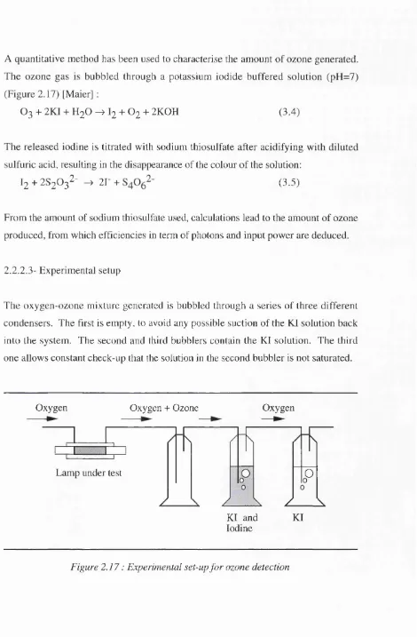
Chapters ...Initial Applications of Excimer Lamps 74 1.- ...Photochem ical generation of ozone 75
1.1- ...Fundamentals of ozone generation 75 1.2- ... Ozone generation with UV radiation 79
1.3- The VUV enhanced ozone reactor 82
1.4- C o n clu sio n 90
2.- ...Application of excimer lamps to MOD 91
2.1- ...Experim ental set-up 91 2.2- ... UV induced metal depositions 93 2.3- ... UV induced dielectric material depositions 96 2.4- ... C o n clu sio n 100
References to chapter 3 101
Chapter 4 ... The Photochemical Deposition and
Characterisation of Silicon Dioxide Layers 103
1 - ... The photo-CVD o f silicon dioxide
from silane and nitrous oxide gas mixtures 104
1.1- ... Experimental conditions 104 1.2- ... Results and discussion 110
1.3- C o n clu sio n 118
2- ... The photo-CVD of silicon dioxide
from silane and oxygen gas mixtures 120
2.1- ... In tro d u ctio n 120 2.2- ... Experimental details and sample preparation 121 2.3- ... Results and discussion 125 2.4- ... C o n clu sio n 135
References to chapter 4 137
Chapters ...The Photochemical Deposition and
Characterisation of Silicon Nitride and Oxynitride Layers 140
1.- The photo-CVD of silicon nitride
from silane and ammonia gas mixtures 141
1 . 1 - ... ...In tro d u ctio n 141 1.2- ... ... Experim ental details 142 1.3- .... ... The window fogging problem 146 1.4- ... ... Growth kinetics 154
1.5- ... 158
2.- The in -s itu photo-CVD of
silicon oxide-nitride-oxide m ultilayers 169
2.1- ...In te re st 169
2.2- Experimental Conditions 169
2.3- SIMS analysis 169
3 - The photo-CVD of silicon oxynitride SiO xNy \q i
3.1- ...Interests in silicon oxynitride 171 3.2- ... Thin SiO^Ny film deposition 171 3.3- ... C o n clu sio n 175
References to chapter 5 176
C o n c lu sio n s 180
Appendix 1 ...The photochemical deposition of a-Si:H
using an argon excimer lamp 183
1.- ...Hydrogenated amorphous silicon (a-Si:H) 183 2.- ...Photo-CVD o f a-Si:H 188
3- Thin Film deposition 192
4.- Conclusions and improvements 201
References to appendix 1 202
Appendix 2... Colours presented by silicon dioxide films
(in perpendicular white light) 204
Appendix 3 ...Assignments o f the principal infra-red
features for the study of thin silicon dielectric films 205
Appendix 4 ... Estimation of the error on Vq 207
Appendix 5 ... List of publications based on this work 209
Introduction
The level of world-wide research linked with the densification of integrated circuits down to ultra large scale integration (ULSI) has burgeoned in recent years indicating without any doubt the enormous potential of this proposed research field. Because of the inherent problems associated with high temperature processing for thin film deposition, low temperature processing is extremely important for a multitude of future generation devices in related technologies. Among the numerous techniques which have been brought out to reduce this “thermal budget”, photo-CVD has many advantages because of its properties (spatial resolution, chemical specificity, and absence of ion damage to the film).
These photo assisted processes have attracted strong interest in recent years by enabling the possibility of producing many types of high quality dielectric and semiconducting film compounds at low temperature. This is appealing for many technologies such as micro-electronics, opto-electronics, magnetic films and other multilayer film systems. During this work at UCL, a new kind of excimer lamp has been developed, capable of producing at high power very energetic photons (up to 9.8eV). This project involves the design and the use of these lamps to initiate photo deposition of various materials. The principle of light emission from excited àimer
The interest in photo assisted techniques stems from the ability of optical radiation to induce specific chemical reactions in the gas phase or at a surface. The selective, optical production of atoms, molecular radical species in the vicinity of a surface, and the ability to do so independently of the substrate temperature, largely decouples temperature effects from the production of the species of interest. In other words, the introduction of photons into a thin film deposition reactor allows one to drive the chemical environment far from equilibrium by selectively producing species that are not normally present in significant concentrations in conventional CVD, MBE or MOCVD reactors. This flexibility inherent with the photo-deposition of films permits operation at lower temperatures. The variety of materials that can be deposited by photo-CVD processes is truly remarkable: to date, some 24 elements, in addition to at least 2 0 insulator and semiconductor compound films have been deposited in this way
[Eden], using various optical radiation from lasers or lamps. However, the use of excimer lamps for photo-CVD is exceptionally new. Excimer lamps, with their capability of emitting tunable wavelengths in the vacuum ultraviolet range (VUV: below 2 0 0nm) could potentially enable better quality films and devices to be made at
lower temperatures than with conventional photo-CVD reactors. Since most precursor gas molecules exhibit an appreciable absorption spectrum in the vacuum UV range, a wide range of compounds can be deposited. For silicon dioxide (Si0 2 )
and silicon nitride (SigN^y mixtures of silane, nitrous oxide, ammonia, and oxygen (SiH^, N2O, NH3, O2) were studied.
This project concentrates on novel applications of excimer lamps to the photo enhanced deposition of thin films. At first the deposition of ShO^ using SiH^ and N2O as precursors has been performed. This work constituted the first application of
an excimer lamp to the deposition of silicon dielectric films. A xenon excimer lamp, which radiates at 172nm, was used to photochemically activate the nitrous oxide precursor. The properties of the layers obtained on our prototype system gives evidence of promising new domains of application for these light sources. The technique is expanded to the deposition of silicon nitride (SigN^;,) layers using ammonia and silane as precursors, as well as that of silicon oxynitride and oxide- nitride-oxide stacked layers. Fast deposition (up to 500Â/min) of was also achieved by irradiating silane and oxygen gas mixtures. Investigations into the
deposition photochemistry are reported, together with the characterisation of the deposited material properties. Good Si0 2 and SigN^ film quality was obtained, as
well as a very good control of the stoichiometry in the case of silicon oxynitride film deposition, therefore providing interesting perspectives for electronic and optical applications.
This thesis is divided into 5 parts. In chapter 1, the photo-chemical vapour deposition is presented, as a technique allowing films to be deposited at low temperatures for semiconductor applications. The description of the photo-CVD reactor developed at UCL is given, together with a short review on the characterisation techniques used. The importance of well understanding the theory of excimers as the main precursor in this technique leads to chapter 2. In particular, the wide range of radiations that can be emitted with such lamps is presented. Various devices are described, enabling the generation of excimer continua from 308nm (xenon chloride), down to 126nm (pur argon). The possibilities offered by the excimer lamps available at UCL are reviewed, in terms of geometry and power output, and a few techniques allowing the measurement of VUV radiations are presented. Chapter 3 concentrates on two direct applications of the ultraviolet radiation. In fact, since a new type of vacuum ultraviolet source became available during this project, new areas of application were investigated, namely the direct VUV enhanced generation of ozone, as well as various other applications of the UV enhanced organometallic technique (MOD). In fact, at the time of writing this thesis, a new project is about to begin at UCL to further extend those MOD experiments.
The photo-CVD of silicon dioxide films from gaseous precursors is presented in
Further to this work, the recent use of devices generating shorter wavelengths, namely the 126nm continuum of argon, has been studied in order to enhance the direct photo-dissociation of silane to deposit hydrogenated amorphous silicon (a-Si:H) layers. Since those results showed some interests, they are presented in
appendix 1.
Reference: J.G. Eden, in Photochemical vapour deposition, Vol. 122 o f “Chemical analysis”, John Wiley & Sons, Inc., New york (1992).
Chapter 1
Photo-CVD, Apparatus and Methods
1- Introduction to photo-chemical vapour deposition
processing (photo-CVD)
1.1- The need for low temperature techniques
Thin dielectric films are of importance in their use as passivating and insulating layers on integrated devices and protecting the active parts of devices from dust and moisture. Over the last decade many different techniques of growth and deposition have been developed to produce these thin films. However, current trends to reduced device geometries and the growing importance of temperature sensitive materials such as III-V semiconductors means that high temperatures cannot be applied to semiconductor processing if all these materials are to be used in a single integrated circuit. One of the problems is that the group V elements from these materials can hardly be processed at temperatures higher than 300°C [Chang]. Clearly, in order to accommodate this step into current device fabrication procedures, the deposition of dielectric materials has to be processed at low temperature. Various techniques have been developed, according to the fact that suppressing the temperature means bringing energy in a different form.
1.2- A brief outline on other techniques
1.2.1 Physical Vapour Deposition (PVD)
This technique relies on the condensation of vapour phase molecules onto a nearest substrate. Evaporation and sputtering are two well known forms of PVD. Conventional resistive evaporation is not useful because at the elevated temperature used the deposited films can be contaminated by the metal from the filament. In case of sputtering, however, ions are directly generated from a plasma, e.g., in Argon. The target and the substrate are located on each of the electrodes, and three types of plasma can be generated: DC sputtering, RE sputtering and magnetron sputtering. The DC sputtering is generally not used for dielectric materials because of its tendency to implant charged particles. For RE sputtering, this effect is compensated on each alternate cycle and hence is more suitable. In magnetron sputtering, plasma
electrons are created by a magnetic field and accelerated to the target. This method gives higher deposition rates. Generally, PVD does not produce good quality dielectric films due to poor stoichiometry and adhesion. They also have poor electrical characteristics.
1.2.2- Chemical Vapour Deposition (CVD)
In CVD, the formation of thin films depends on the surface reaction that occurs between the surface atoms of the substrate and the chemical species that arrive on it from the gas phase. High temperature CVD (for Si0 2 : 700 to 1100°C) gives very
good quality films. These dielectrics are stoichiometric and do not contain hydrogen [Pliskin].
The tendency to reduce the temperature has developed a technique where electrical energy is provided to dissociate gas phase molecules. This form is called Plasma- Enhanced-Chemical Vapour Deposition (PECVD). The sample is located on one grounded electrode, and a high voltage RF signal (typically 13. S'^ MHz) is applied to the other electrode facing the substrate. This causes electrical discharges between the plates producing a plasma which breaks up the source gas molecules into radicals, ions, and other energetic species. The substrate temperature used can consequently be reduced (from 400°C to room temperature), but charged or high kinetic energy species can be the cause of bombardment of the sample which is detrimental to interface sensitive devices [Vinckier] [Buchanan].
1.3- Photo-enhanced Chemical Vapour Deposition
1.3.1- Generalities
of photochemically dissociating a gas for thin film material deposition. Many light sources have been used from powerful lasers to lamps. The energy provided from the photons can be used in various ways for the deposition of thin films, the most frequent way being the photolytic dissociation of reactant gases. This direct photolysis is defined from the interaction of one photon with one gas phase molecule. The excited molecule liberates its energy by breaking into different molecules or radicals which may be used in the film growth process. Generally only ultraviolet (UV) photons can provide enough energy for direct photolysis.
The dissociation of the molecule can also be caused by the collision with an excited species which required less energy than that necessary for direct photolysis. This is called photo-sensitisation and has been extensively used with mercury lamps [Peters] [Saitoh] [Tarui-1983]. Powerful lasers can also enhance multiphoton photolysis or pyrolytic dissociation [Boyer-1982, -1984] [Fogarassy]. Figure 1.1 shows a variety of configurations used for photo-CVD reactors.
1.3.2- Photo-deposition of dielectric materials.
Photo-CVD techniques are low temperature techniques (from 350°C to room temperature) which do not present the drawback effect of surface bombardment with high energetic species. These techniques have been applied in various ways to the deposition of dielectric materials on substrates. In the case of silicon dioxide (Si0 2 ),
the most frequently used dielectric material for gate oxides and passivating layers, two reaction schemes are possible:
• Oxidation, allowing growth of Si0 2 by the oxidation of the surface layer of silicon,
• Deposition, achieved when both silicon and oxygen radicals are brought together and allowed to react on the substrate surface.
Generally, the oxidation route gives better quality Si-Si0 2 interfaces due to its inner
volume characteristic, but it is obviously restricted to silicon substrates. The deposition technique is preferred for the deposition thick passivating layers on various materials.
UV Lamps
P r e s s u r e ind. c a p acitan ce m a n o m e te r
Sample
Lam p co n tro lle r AC p o w er
M ass flow box
[Licoppe]
.At Ret le c to r
/ Low P ressu re Hg Larrp
&
Scprasd"3^R eactor
SIH^
Sut>strate (OG
RP
[Tarui-1984]
lo w -p ressu re m ercu ry lam p sy n th etic q u artz
tu b e
' ■ NHg n o zzle
sa m p le ^ ... "(: 1mm
boat
[Nayar] [Ishikawa] tu n g s te n h alo g en lam p
l a m p I
s u p p l y 1 I
S 1 H 4
— - = j m f c | = :
[Baker] [Bhatnagar]
l a m p Po^wcr Supply — C ooling WiiCT
Cu AND T F E MIXING MAN I f OLD
ORINO SEAL B S
GAS FLOW CONTROL CTU LENS
t e l e s c o p e Si SUBSTRATE
TO VACUUM
TurtM /Rotixy P um pt
[Patel-1990] [Boyer-1982]
[Nishino] [Tsuji]
MASS FLOW
CONTROLLER
G as N ozzte
Pow er M eter
S u b s tra te
S y n th etic F used Q uartz C y lin d rical L en s
^ 1
L a s e r Beam H e a te r
• Vacuum Pum p
WAFER
LASER
R O TA RY
HEATER
The principle of the deposition technique is to have a gas phase reaction between Si and oxygen radicals. The commonly used precursors for these reactions are silicon hydrides such as silane (SiH^), disilane (Si2H^) or trisilane (SigHg), and for the
oxygen radicals molecular oxygen (O2), nitrous oxide (N2O) or nitrogen dioxide
(NO2) can be used. The photon source used has to dissociate these precursors. A
look at absorption cross section data [Itoh] [Okabe] [Calvert] [Baulch], showed that radiations below 200nm are suitable. This domain of ultra-violet is called Vacuum Ultra-Violet (VUV) according to its absorption in oxygen, and hence in air.
The sources of photons to be used for direct photo-CVD techniques on various substrates for dielectric materials have then to provide high energy photons close to, or in the Vacuum Ultra-Violet range (Table 1.1).
VUV
' / / / / / / / / / / / / ,
UV
B
+
Visible
200 nm
300 nm
400 nm
Table 1.1 : Wavelength location o f the UV ranges
1.4- Sources of Vacuum Ultraviolet light
1.4.1- Lamps
Owing to the high absorbance of air, early spectroscopic studies in the ultraviolet region of the spectrum were limited to wavelengths longer than about 2000Â. In 1893, Viktor Schumann built the first vacuum spectrograph and made the first investigation of vacuum ultraviolet radiation. In 1906, Theodore Lyman, using a vacuum spectrograph equipped with a concave diffraction grating, was the first to measure wavelengths in this region. He found that the Schumann's spectrum had a
short wavelength limit of about 125nm, the limit due to the transmission characteristics of the fluorite material used. The region 200 to 125Â is since known as the Schumann region [Samson]. This is our wavelength range of interest.
Several gas discharge sources can emit in the vacuum ultraviolet range (cf. table 1.2). The low pressure mercury lamp (germicidal lamp) is by far the most widely used UV lamp [Phillips]. In the short wavelength range, its spectrum consists of 2 lines centred at 254nm and 185nm. The total UV efficiency can reach 50%; a very high value for such an energetic radiation. However, the 185nm line efficiency hardly reaches 10 % of the 254nm line, and implies the use of expensive window materials. When shorter wavelengths are required, low pressure discharge lamps and internal lamps have been used [Tarui-1984] [Robertson] [Marks] [Patel]. The conversion efficiency of these sources is however very low as can be seen in table 1.2. This point is discussed in detail in chapter 2.
Discharge medium Wavelength (nm) Efficiency (%)
Mercury (Low Pressure) 185, 254 50
Hydrogen, Deuterium 100- 300 0.33, 0.05
Nitrogen 120-130 0.08
Glow discharge in
Argon 105-135 « 0 . 0 1
Krypton 125- 170 - 0 . 0 1
Xenon 150-180 « 0 . 0 1
Table 1.2 : VUV sources
Materials Cut off Wavelength (nm)
Cost
(£/cm^) Comments
LiF 105 1 0 hydroscopic
MgF^ 115 30 hardly soluble in HF
Sapphire 142 15
Crystalline quartz 160 1
fused quartz (Suprasil®) 160 1 non crystalline (!)
Table 1.3 : Vacuum ultraviolet materials
1.4.2- Lasers
Lasers have also been used as VUV sources of photons. Excimer lasers are powerful coherent sources of short wavelength UV photons [Rhodes]. Generally pulsed, they can provide energies of lOOmJ per pulse at frequencies up to lOOHz. The most commonly used excimer lasers commercially available are using rare gas-halogen mixtures with limited photon energy radiation (KrF, 248nm or ArF, 193nm). Shorter wavelengths may be obtained with pure rare gas excimer lasers, but these are, so far, only used as laboratory devices, because of the very high energy necessary for pumping these gases to inversion and the very high gas purity required. We can quote however the recent pure Argon laser emitting 80mJ at 126nm developed by Kurosawa et al. [Kurosawa].
The price of excimer lasers is by no mean comparable with those of lamps (e.g., typical number for capital cost: «£30k). The costs to safely operate (e.g., gases, power, mirrors & protective coatings) and handle these powerful low wavelength radiations are high.
1.4.3- Excimer Lamps
Recently, a new kind of UV lamp has been reported [Kogelschatz]. Experimentally developed in a Swiss Company, Asea Brown Boveri (ABB), this new generation of ultraviolet lamps work on the principle of excimer discharge generation. To date, they are not commercially available and have never been used experimentally for the photo-CVD of dielectric materials. As for the previously described UV lamps, the principle relies on an electrical discharge of a plasma gas. However, and this is the distinctive feature of these lamps, the efficiency of light generation can theoretically reach 40%. Experimental efficiencies as high as 10% have been reported [Gellert]. They cover a wide range of wavelengths from visible to VUV. These sources are therefore very attractive for photo-enhanced CVD (table 1.4).
The aim of this project, which was sponsored primarily by ABB, is to develop new prototypes of those light emitting devices, and then to exploit their potential for the photo-chemical vapour deposition of thin films. The whole of Chapter 2 will be dedicated to the presentation of these new lamp features.
Discharge medium Wavelength (nm) Efficiency (%) Excimer discharge in
Argon 126
Krypton 146 - 1 0%
Xenon 172
2.- Design of a photo-Chemical Vapour Deposition
reactor
At the time of the first drawings for the construction of this vacuum system, there was no precise idea on the shapes, sizes and powers to be available from the light sources. The main objectives were to build a very flexible system to host very different photon sources. Here is presented in detail the deposition reactor, in terms of geometry and incorporated features, namely the substrate holder/heater, the precursor gas feeding control and the pumping apparatus. Also, since the next chapter will be concentrating on the UV source, only a minimum description of the parts incorporating the light source is given here.
2.1- Stipulations
A photo-CVD plant is generally composed of a combination of a light source, gas distribution equipment, a processing chamber, various in-situ diagnosis apparatus, and a pumping unit. According to the geometry of the processing chamber and to the size of the samples required, various configurations are possible for the light handling. Two main families of reactors can be denoted depending on whether the process uses focused light or not. Generally lamps are used in perpendicular illumination mode which allows the deposition of thin films on large areas with a very good homogeneity [Su] [Petitjean]. Lasers have been used for silicon dioxide growth either under parallel [Boyer-1982] [Szorényi] or perpendicular modes [Nayar], the former allowing the exposition of a gas phase to the photon flux without bombarding the sample surface, the latter being more appropriate with writing, etching or ablating techniques. The laser light beams can moreover be focused to offer on smaller size coverage much higher energies.
For direct photolysis, lamps providing very short wavelengths (^<300nm) are used, and only the photolytic power hv of the photons is used. In our case, where the light source emits high energy photons (l<2 0 0nm) and over a uniform surface, there is no
need for focusing the light beam. The configuration which was chosen allows parallel illumination of the sample surface, on sizes up to one inch in diameter.
To allow further flexibility in the material to be deposited, the design of the reactor offers different processing gas lines, including silane (SiH^), nitrous oxide (N2O),
ammonia (NH3) and oxygen (O2). The pumping system provides a high vacuum for
sample preparation, as well as a high pumping speed during processing when high precursor fluxes are used.
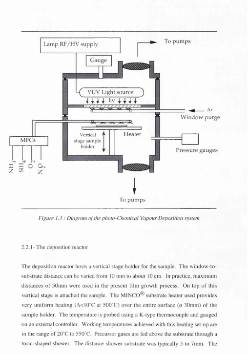
2.2- General diagram of the photo-CVD reactor
Figure 1.2 shows a view of the entire system. The vacuum chamber is located on the left, whether the electrical apparatus including readout and control equipments are incorporated on a vertical rack on the right handside of the system. The gas handling is located outside the room for safety requirements, and one of the four gas feeding mass flow controllers appears in the background of the system on the right hand side. The vacuum system is built from stainless steel vacuum components (figure 1.3). It consists of the superposition of two chambers separated by a window transparent to the light radiation. The top chamber hosts the light source, whether the bottom chamber is the deposition reactor. According to the fact that light radiations well below the air cut-off are to be used, the top chamber has to be kept under vacuum. The processing chamber offers an ultraclean environment for sample preparation prior to deposition with background pressures of 10"^ mbar. Access to the sample stage implies the removal of the lamp chamber and the breaking of the vacuum.
k
Figure 1.2 : Views o f the photo-CVD system at UCL (Entire system (top), Deposition reactor (bottom))
To pum ps Lamp RF/H V supply
VUV Light source
j
U i i
hv i 4 I 4
Heater
V ertical t
sta g e sa m p le h old er
MFCs
W indow purge
Pressure gauges
CO fN
!Ih O Qn
Z ^ 2
To pum ps
Figure 1.3 : Diagram of the photo-Chemical Vapour Deposition system
2.2.1- The deposition reactor
The deposition reactor hosts a vertical stage holder for the sample. The window-to- substrate distance can be varied from 10 mm to about 10 cm. In practice, maximum distances of 50mm were used in the present film growth process. On top of this vertical stage is attached the sample. The MINGO® substrate heater used provides very uniform heating (A<10°C at 500°C) over the entire surface ( 0 30mm) of the
flows of the precursor gases entering the chamber are controlled by a set of 4 thermal mass flow controllers (MFC). The nitrogen ranges of the flow controllers are of 20, 200, 200 and 200 seem (Standard Cubic Centimetre per Minute (25°C, 760 torr)) for silane, nitrous oxide, ammonia and oxygen respectively. The MFCs are controlled using a MKS remote unit allowing 4 channel power supply/readout with gas correction potentiometers and set point signal for each channel. From those, the gas precursors are directly fed to the in-situ shower through a 1/4 inch pipe, the latter has the potential of being heated up to about 100°C to study the effect of warming the precursors.
A gas purge shower is placed facing the window separating the two chambers. This enables the use of a transparent gas such as argon during deposition to flush any precursor away from the window. The shower consists of a very thin perforated stainless steel straw (02mm). This apparatus is required for the deposition of materials that show a high cross section to the radiation used during their deposition. It is of particular use in the cases of silicon nitride and amorphous silicon. In some cases, however, (in particular for silicon dioxide which hardly absorbs radiations above 165nm), a good control of the pressure and the flow of the gas precursors can be sufficient to limit the deposition on the window. Window purging is therefore not recommended in these cases as it can cause flow perturbations which alter the experimental conditions. This problem will be discussed in detail in chapter 4 and 5 when depositions are presented.
2.2.2- The lamp chamber
Depending on the required lamp configuration, this chamber has to offer a wide range of possibilities for holding a lamp device. As the chamber configuration is in turn dependent on the type of lamp used, it is appropriate to describe it after the discussion of the lamps which is presented in chapter 2. Here is only mentioned that this vacuum chamber offers electrical feedthrough features, viewports and pressure gauges.
2.2.3- VUV transparent window.
The window separating the two chambers has to offer a very low photon cut-off, as well as mechanical resistance to the possible pressure difference between the chambers. As presented in table 1.3, some quartz materials fit applications using wavelengths as low as 160nm. However, as lower radiations may have to be used, the window will have to be crystalline magnesium fluoride (Mgp2) or lithium fluoride
(LiF). Furthermore, the use of a fluorinated saturated compound allows eventual cleaning with fluoridric acid, good remover of materials such as silicon dioxide that are to be deposited. Mgp2 was chosen, although more expensive than LiF, since it
has the advantages of being for being not hygroscopic and therefore more stable to successive cleanings.
At the early stages of this project we bought a magnesium fluoride viewport supplied by a vacuum company. Despite the high cost of these windows mainly due to UHV sealing requirements, they unfortunately do not offer mechanical resistance to an inverted pressure gradient. In fact, a pressure difference of 1 atmosphere in the “wrong” direction was sufficient to unseal it.
I
therefore recommend buying the window from a crystal growing company and to assemble it to any home made flange ensuring vacuum with a compressed seal (figure 1.4).Compression
fitting
Thick Washer Magnesium fluoride window
The minimum thickness of the window is calculated with K P D
Thick ^ = . 1 ^ — (1 1 )
where S is the apparent elastic limit of the material, D the unsupported diameter, P the differential pressure, and K a coefficient that incorporates a minimum safety factor.
2.2.4- Vacuum apparatus
The pumping set-up offers high vacuum background pressures (10“^ mbar) from a water cooled turbomol ecular pump (170 1/s), backed up with a miniature double stage rotary pump (30 1/min). In parallel to this stage is a high pumping speed fomblinised rotary pump (540 1/min). This pump is used during deposition to maintain the chamber pressure constant when the precursor gases are fed into the reactor. Also, due to the very small pumping speed of the miniature backing pump, the 5401/min rotary pump is also used to provide primary vacuum before turbomollecular pumping. Figure 1.5 gives a schematic diagram of the pumping set up. The entire unit complies with any of the following scenario:
• it allows permanent high vacuum pumping of both the reactor and the lamp chamber between deposition experiments
• it allows during processing the pumping at high speed of the gas precursors fed into the deposition reactor while the lamp chamber is maintained at a constant
pressure
• it allows the purge of the lamp discharge gas in the top chamber without stopping high vacuum pumping in the reactor
• it ensures insulation of the turbomollecular pump during deposition to avoid its contamination with the precursor chemicals.
The pressures are measured with 3 gauges. In order to achieve high accuracy in the measurement of the medium pressure lamp discharge and the use of corrosive precursor chemicals in the reactor, the system is equipped with two capacitance manometers ranging 1000 to 10“^ mbar and 10 to 10“^ mbar respectively. A third pressure device consisting of a Penning gauge combined with a pirani is finally used to monitor the high vacuum background pressure in the reactor.
Precursor gases —
Gate Valve Lamp Chamber Processing Reactor VI V4
X
V5© / ) m % a r pump
V
M
V3Lamp Discharge Gases
0 . 1 to 1 0 0 0 mbar range
"^capacitance pressure gauge
Rotary Pump (3 0 1/min)
Rotary Pump (5401/min)
0 . 0 0 1 to 1 0 mbar
range capacitance pressure gauge + Penning and Pirani
gauges
Figure 1.5 : Pumping setup
2.2.5- VUV and UV monochromator
2.3- Safety requirements
The use of toxic and dangerous chemicals such as ammonia and silane has required the use of various safety apparatus to prevent any experimental mishandling. In particular, the silane is pyrophoric and therefore has to be handled with particular care. In the pure gas phase, it is thermally stable up to 200°C, but small leaks of the gas into air will spontaneously ignite to give clouds of white amorphous silica particles. Large leaks can lead to an unstable cloud of gas which will suddenly explode with no preflame [Tucker]. Pure silane was used, in order to avoid any eventual diluting gas experimental artefact. Also, when pure silane is used, the risks are reduced by the much lower pressures of silane involved and the considerable reduction in the amounts of gas required for each individual experiment. In fact, the very low silane flows employed often made possible the work on a closed silane cylinder after having filled only the feeding line.
In terms of safety, the gas handling has to be contemplated separately whether the presence of silane is considered at high pressures before the reactor, or at atmospheric pressures getting in contact with air after the pumps.
2.3.1- From cylinder to reactor
In most of the pipes and fittings of the supply lines, the pressures used are higher than atmospheric. It is essential to prevent any faulty action of a valve that could leak hazardous gas into the laboratory or to another apparatus. As such, an automatic shut off valve is located on the silane cylinder, to act as a flow limiting device to cut the gas supply if the flow happens to exceed a critical value of 7 LPM (Standard Litre per Minute (2TC, 17 PSIN2)). A set of three other normally closed air actuated valves,
locked with key-actuated switches, is used from the cylinder to the mass flow controllers and finally to the reactor (figure 1.6).
Locked Solenoid
O - u
M FC C ontroller
Locked Solenoids (x3)
0 - n [ Z ^
-I
>
T3
: 0
Pi
Extracted Gas Cabinet _Lockedjind ojts^ejaboratqiy j
MFC
Deposition System
Air actuated Valves (x3) (+ remote command)
Figure 1.6 : Gas Handling system (Only the case o f silane is drawn)
2.3.2- Exhaust gas handling
Because the reactant gases are pumped away from the system, toxic and hazardous residual gases will be present in the pumps at possibly high temperatures and released into the atmosphere after the pump. In fact, unreacted silane in the exhaust system, particularly if H2 is present, can lead to exhaust fires [Hammond]. To prevent such a
problem, the exhaust system of the pump is connected to an extractor, and during use the pump is heavily purged (about 1 0 0 0 times the incoming silane flow) with an inert
gas. This inert gas purge is introduced into the ballast of the two stage rotary pump in order to dilute the actual content of the gas in the pump without affecting its pumping speed.
2.4- Maintenance
3.- Characterisation of the deposited thin films
In this section are presented the experimental characterisation techniques used during this project to analyse the photo-deposited thin film layers. The thicknesses (a few hundred Angstroms) and refracti-ze indices were measured using ellipsometry. The background principles of the technique are presented, and the level of accuracy obtained in these measurements is discussed. To further study the physical characteristics of the deposited films, Infra-Red spectroscopy was used. This technique offers a way to analyse the concentration of the species present in the film from their binding vibration modes. In particular, Fourier Transformed Infra Red Spectroscopy (FTIR) will be discussed.
3.1- Ellipsometry
Ellipsometry is a non-destructive optical analysis method, based on the measurement of a change in the polarisation state of an incident light when refracted on a surface.
The measure of this change in polarisation gives:
• either optical parameters of a reflecting surface if the latter is not covered by any film,
• or the thickness and optical properties of a layer covering a reflecting surface,
• or in the case of spectroscopic ellipsometry (wavelength variation of the incident beam), the optical characteristics of the transient region between substrate and
thin film.
In the case of ellipsometry measurements, the parameters concerned are: • The refractive index, n, refraction parameter of the incident radiation,
• The absorption coefficient, k, optical attenuation of a beam while traversing a medium.
n and k are directly dependent on the wavelength of the light beam used, e.g., a Helium-Neon laser source radiating at 632.8nm. Thin dielectric films generally show a very low reflectivity, and most of them are transparent (k=0) in a broad region of
the spectrum.
3.1.1- Fundamental equation of ellipsometry
For this discussion, the incident and reflected beams are invoked by their electrical components E//, Ej_ and E”//, E”j^ projected in the incident (//) and the perpendicular (_L) plane respectively (see figure 1.7). Ellipsometry enables the measurement of the difference in polarisation of the light beam after reflection. These measures give the phase shift (A) and the ratio (tan \\r) between the peak values of the // and _L components of the reflected beam.
It comes:
| E"// I | E / / |
(1.2)
IË7~
I
The reflection on the surface causes a different phase shift in the // and _L waves which are designated by A// and Aj_ respectively, and:
A = A// - Aj_ (1.3)
E "//
The ratio p = can then be expressed with:
p = tan Y e ^ (1 4 )
with 0 ° < 'F < 9 0 ° an d 0 < A < 360°.
He-Ne Laser 6328 Jl
Beam Attenuator Analyser Module
Analyser prism (rotatable) Polariser prism
(rotatable)
E// E i
Ambient Medium (nO,kO) ""-L Thin Film (e, n l, kl)
Substrate (n2,k2)
Figure 1.7 : Schematic diagram of ellipsometry
3.1.2- Characterisation of a thin film with ellipsometry
An ellipsometric measurement involves irradiating the surface of a sample at a known angle of incidence O with a collimated beam of monochromatic light having a known, controllable state of polarisation, and determining the differences between the states of polarisation of the incident and reflected beams caused by the sample. A and Y are directly obtained from the measure of the angular azimuths of the polariser and the analyser respectively when the light extinction condition is obtained. A and Y are cyclic functions of the film thickness, and the cyclic function reaches the starting point when the optical path is a multiple of the light wavelength.
In the last century, Fresnel derived equations for the reflection of light from a film- free surface, establishing that A and Y are each functions of the angle of incidence O, the wavelength of the light, the refractive index nQ of the ambient medium, as well as the real part U2 and the imaginary part k2 of the substrate refractive index. Drude
extended the Fresnel reflection equations to a single-film model where A and Y depend on the real part n ^ and the imaginary part k j of the film refractive index and on the film thickness e. Namely:
A = f2 (O, X, iiQ, Ü2, k2 , n j, k^, e) (1.5)
T = g2 ( 0 , X, tiQ, Ü2, k2, n j, k^, e) (1.6)
The angle of incidence 0 = 70°, and the medium refractive index nQ are constant, and in the case of thin films on silicon, n2» k2 are also constants at ^=632.8nm. From
the measure of A and 'F, and as the optical constants of the substrate are known, it is possible to determine the values of the thickness and the refractive index of the film, within the limits of a periodic constant. Practically, either graphical methods or computerised calculations can be used. In the case of silicon oxide or nitride thin films on silicon, the cycle thickness is 2815Â and 1792Â respectively. For most of the experiments, the deposited layers have thicknesses well below these values. However, if the deposited films were sufficiently thick to reach these values, the colour of the sample gives a good idea of the thickness (see Appendix 2), enabling the determination of the cycle.
3.1.3- Precision and accuracy
3.2- Infra-red spectrometry
3.2.1- Interest
Infra-red spectroscopy is a well known technique for structural analysis of materials. In the case of silicon and silicon dielectrics, the optical absorption measurements in the infra-red region can yield important information about the film such as thickness, chemical composition, density and impurity concentrations. The measurements were performed on films deposited on single crystal silicon wafer substrates, which are transparent over the spectral range of interest (25|Lim to 2 .5 |im , corresponding to 400 to 4000cm" ^). Absorption in the near infra-red region is due to vibrational mode resonance of the inter-atomic bonds in the material. Different vibrational modes and bonds between different elements, give rise to a range of characteristic absorption frequencies associated with each bond type. Appendix 3 gives a review of the usual infra-red vibrational mode for several silicon bonded light elements, which are of interest in this work.
3.2.2- Instruments
3.2.2.1- Dual beam spectrophotometers
At the early stages of this project, a Perkin Elmer 380 dual beam spectrophotometer, which scans over the range 200 cm"^ to 4000 cm“^ was used. The infra-red radiation source in this instrument is a red hot silicon carbide rod, which illuminates both the coated sample and the bare silicon substrate reference. The transmitted radiation through each sample is alternately reflected, via a diffraction grating, onto a pyroelectric sensor by a rotating mirror. The ratio of the two signals at a given wavenumber then defines the transmission through the coated sample relative to the reference. The diffraction grating slowly sweeps the detected infra-red radiation over the desired wavenumber range and a chart recorder plots out the transmission spectrum during the scan. However, those instruments are far from being as convenient as modern instruments using Fourier Transform Infra-Red spectroscopy (FTIR).
3.2.2.2- Fourier Transform Infrared Spectroscopy (FTIR)
FTIR spectroscopy offers potential advantages compared with conventional dispersion infra-red spectroscopy, namely:
• Higher signal to noise ratios for spectra obtained under conditions of equal measurement time, (only a few seconds per scan),
• Higher accuracy in frequency for spectra taken over a wide range of frequencies,
• Fewer difficulties with insufficient sample size.
An FTIR spectrometer basically consists of two parts: an optical system which uses an interferometer, and a dedicated computer. The computer controls optical components, collects and stores data, performs computation on data, and displays spectra. The use of a dedicated computer with any spectrometer has advantages. However, the real advantages of an FTIR spectrometer result in the use of an interferometer rather than a grating or prism. Figure 1.8 shows a simplified diagram of the optical system.
Laser Reference Interferometer
Detector Detector
Sample
Source
Infra-red Interferometer
The light from an infra-red source is collimated and sent to the beam splitter of a Michelson interferometer. The beam is divided, part going to the moving mirror and part to the fixed mirror. The return beams recombine at the beam splitter undergoing interference. The reconstructed beam is then directed through the sample and focused onto the detector. A laser beam, undergoing the same change of optical path as the infrared beam, serves to reference the position of the mirror during the scan, and initiates the collection of data points from the signal of the infrared detector at uniform intervals of mirror travel. The data points are digitized by an analog-to-digital converter and stored in a computer memory. The result is an interferogram, i.e., a record of the signal of the infra-red detector as a function of the difference in path (retardation) for the two beams in the interferometer. The interferometer scans are generally taken quite rapidly (a few seconds each) to avoid extensive signal averaging before digitalisation. Data from additional scans can be coadded to the data stored in computer memory to improve the signal to noise ratio of the interferogram. A Fourier transformation is performed on the interferogram using a fast Fourier transform algorithm, to convert the signal as a function of retardation to a signal as a function of frequency. Two different FTIR spectrometers have been used during this project. Part of the results in Chapter 4 and 5 are either computed from a Nicolet 200 spectrometer, or from a Perkin-Elmer 7000 model.
4.- Conclusion
The context into which enters the photo-CVD technique has been presented. The inherent necessity associated with the use of low temperatures during thin film processing make these processes good candidates towards future industrial applications. The interest in photo-CVD techniques stems from the ability of optical radiation to induce specific chemical reactions in the gas phase or at a surface. The development of a new kind of lamps, namely the excimer lamps, capable of producing high fluxes of photons in the VUV region, opens up new applications towards the direct photo-initiated deposition of thin films.
The photo-CVD reactor, which has been developed at UCL during this project has been presented. It offers, with a very high flexibility, the possibility to expose substrates and/or gas phases (SiH^, N2 O, NH3 or O2 ), in a high vacuum
References to chapter 1
[Baulch] D.L. Baulch, R.A. Cox, P J. Crutzen, R.F. Hampson, J.A. Kerr, J. Tree, R.T. Watson,
J. Phys. Chem. Ref. Data, 11 (1982) 359
[Boyd] I.W. Boyd, Laser Processing o f Thin Film s and Microstructures, (Springer, New York, 1987)
[Boyer-1982] P.K. Boyer, G.A. Roche, W,H Ritchie and G.J. Collins Appl. Phys. Lett., 40 (1982) 716
[Boyer-1984] P.K. Boyer, K.A. Emery , H. Zamani and G.J. Collins Appl. Phys. Lett., 45 (1984) 979
[Buchanan] D A. Buchanan
Appl. Phys. Lett., 56 (1990), 1037 [Calvert] J.G. Calvert & J.N. Pitts, Photochemistry,
J. Wiley & Sons, New york (1966) [Chang] R.R.Chang, R. Iyer, D.L. Lile
J. Appl. Phys., 61 (1987) 1995
[Eden] J.G. Eden, in Thin film process II, ed. by J.L. Vossen & W. Kern, Academic press, San Diego, CA (1991)
[Emeléus] H.J. Emeléus and K Stewart,
Trans. Faraday Soc., 32 (1936) 1577 [Escher] G.C. Escher,
SPIE Vol. 998 Excimer Beam Applications (1988) 30 [Fogarassy] E. Fogarassy, A. Slaoui, C. Fuchs & J.P. Stoquert
Appl. Surf. Sci., 54 (1992) 180
[GeUert] B. Gellert and U. Kogelschatz, Appl. Phys. B, 53 (1991) 14 [Green] D.W. Green and G.T Reedy,
in Fourier Transform Infrared Spectroscopy, ed. by J R. Ferraro, L.J. Basile, Academic Press, New York, (1978) [Hammond] M.L. Hammond, Solid State Technology, (Dec. 1980) 104 [Itoh] U. Itoh, Y. Toyoshima, H. Onuki, N. Washida, T. Ibuki,
J. Chem. Phys., 85 (1986), 4867
[Kogelschatz] U. Kogelschatz, Appl. Surf. Sci., 54 (1992) 410
[Kurosawa] [Lefevre] [Marks] [Nayar] [Okabe] [Patel] [Peters] [Petitjean] [Phillips] [Pliskin] [Rhodes] [Robertson] [Romeyn] [Saitoh] [Samson] [Su]
K.Kurosawa, Y. Takigawa, W. Sasaki, M. Katto, Y, Inoue Jap. J. Appl. Phys., 30 (1991) 3219
H. Lefevre, M.Schulz, in The Si-Si0 2 system, ed. by P. Balk, ch. 6 (1988)
J. Marks and R.E. Robertson Appl. Phys. Lett. 52 (1988)810
V. Nayar, I.W. Boyd, F.N. Goodall, G. Arthur, Appl. Surf. Sci., 36 (1989) 134
H. Okabe Photochemistry o f small molecules,
John Wiley & Sons (1978) New York P.Patel and I.W. Boyd,
Appl. Surf. Sci., 46 (1990) 352 J.W. Peters
Tech. Dig. IEEE Int. Electron. Dev. Meet., New York, (1981) 240
M. Petitjean, N. Proust, J-F. Chapeaublanc, J. Perrin, Appl. Surf. Sci., 46 (1990) 189
R. Phillips, in “Sources and Applications of Ultraviolet Radiation”, Academic Press, London (1983)
W.A. Pliskin
J. Vac. Sci. Technol., 14 (1977) 1064
Ch.K. Rhodes, Excimer Lasers, Vol. 30 of Topics o f Applied Physics , Springer, Berlin (1984)
P. A. Robertson, The photo-enhanced deposition o f amorphous silicon and silicon oxide thin films,
PhD thesis. University of Cambridge, UK (1987) H. Romeyn, Jr., and W.A. Noyes, Jr.
J. Am. Chem. Soc., 54 (1932) 4143
T. Saitoh, T. Shimada, M. Migitaka, and Y. Tarui J. Non-Cryst. Solids, 59 (1983) 715
J A R. Samson in Techniques o f Vacuum U ltraviolet spectroscopy, John Wiley & Sons, New York (1967)
[Szorényi] T. Szorényi, P. Gonzalez, M.D. Fernandez, J. Pou, B. Léon, M. Pérez-Amor, Thin Soi. Films., 193/194 (1990) 619 [Tarui-1983] Y. Tarui, K. Sorimachi, K. Fujii, K. Aota, T Saitoh
J. Non-Cryst. Solids, 59/60 (1983) 711
[Tarui-1984] Y. Tarui, K. Aota, K. Kamisako, S. Suzuki, T. Hiramoto Ext. Abs. XVI Int. Conf. Sol. State Devices and Materials, Kobe, Japan (1984) 429
[Tucker] B.A. Tucker, Eur. Semicond. Design and Prod., (July 1985) 27 [Vinckier] C. Vinkier, S. de Jaegere
J. Electrochem. Soc., 137 (1990) 628
Chapter 2
Excimer Lamps
1 - Silent discharges for excimer generation
1.1- Electrical discharges for UV generation
1.1.1- History
The luminous emission observed when an electrical current passes through a gas has fascinated observers since their discovery at the very beginning of the study of electricity. Initial investigations of this phenomenon was limited by the low deliverable current initiated by electrostatic machines, and the area of study centred on atmospheric pressure low current breakdown experiments. Also, due to the very dangerous electrical equipment used, the study of the high pressure electrical discharge of lightning proved fatal to far more physicists than it enlightened.
In 1879, long before the concepts of mobility, diffusion, attachment or recombination had been born. Sir William Crookes had already studied the rays emitted from discharges in low pressure glass tubes whilst submitted to DC voltages from voltaic piles. After his long series of experiments, and the design of his many Crookes tubes, he championed the theory that these emitted rays were due to charged particles. With the improvement of vacuum and glass blowing techniques and electricity handling, the behaviour of the glow discharge as a function of pressure, electrode geometry, and type of gas, filled the literature for many years till the discovery of X- rays (1895) and the electron (1896).
It is only by 1911, with the work of J.J. Thomson and J.S. Townsend, that we can really consider the beginning of the historical development of the field of study of the electrical discharge in gases, with the clear recognition of the nature of the elementary charged particles, especially the electron, as well as the concept of positive and negative ions. J.S. Townsend became the acknowledged leader in discharge research of his time. He and his students dominated the field for a generation, amassing an impressive volume of data, coefficients, and parameters to characterise the “passage of electricity through gases”. The knowledge of the electrical discharge in gases considerably advanced during this time to the point where experimentation could not be improved with the equipment of the time.
W ith the great classification of atomic theory together with the remarkable improvements in laboratory techniques through the use of Pyrex glass, better pumps, induction furnaces, electron tubes, and oscillographs, the mid-twentieth century accelerated many types of discharge tubes and plasma research. Engineers introduced these phenomena into everyday life in the form of domestic fluorescent light and neon signs. In the last decade, interest in this field has rapidly increased because of increased activity in atmospheric research and plasma physics.
1.1.2- Electrical discharges
Electrical discharges are transitions of charges through a gas, generating light by radiative decomposition of excited states [Hirsh]. Today intense UV radiations from medium and high pressure glow discharge xenon and mercury/rare gases lamps are generated by the application of a high electric field between two electrodes. In such a way, low wavelengths can be obtained from low pressure rare gas resonance line sources, e.g., the argon line at 106nm [Patel-1990], the Krypton line at 124nm and the Xenon line at 147nm.
However these glow discharges are only accessible at low pressures, which implies that few light-generating excited species exist, and furthermore low pressure often shows self absorption of the emitted light (see details in § 1.2.2). Only low efficiency photon fluxes will therefore be obtained with such devices. For higher fluxes, the gas pressure has to be increased and the type of the discharge changes from glow discharge to arc discharge. For arc discharges, the light generation is caused by a charge transition between the electrodes. Increasing the electric field between two plates to a critical field or breakdown voltage results in the appearance of an arc. The breakdown voltage is directly correlated with the dielectric strength of the gas mixture and is therefore lower for rare gases and it increases with the pressure.
n d (cm"2)
4000 3000
Xe
2 0 0 0
1500
Ar 1000
Ne 800
600
400 300 Xe
N e
2 0 0
0 5 2 5 10 20 50 100 200
p^d ( Torr cm )
Figure 2.1 : Paschen breakdown voltages for rare gases [Meek]
The discharge is a filament within which electrons and ions can migrate from one electrode to the other, in a single channel of excited states. However, when an arc appears in the gap separating the electrodes, the local dielectric strength drops. The arc is thus self-sustained and a very high current passes through the discharge. Heavy bombardment of the electrodes with excited species during an arc discharge results in their gradual erosion. High pressure discharges have therefore to be modified in order to obtain continuous generation of the excited species. These two major problems associated with conventional arc discharges of self-sustaining and electrode eroding tend to limit large scale applications of this mode of photon generation.
1.2- The silent discharge or dielectric barrier discharge
1.2.1- The electrode problem
To prevent the etching of the electrodes during discharge, it is essential to limit the amount of charge and energy that can be fed into the arc. One simple way is to cover the electrodes with a dielectric material (Fig 2.2).
Diel E Plasma EDiel
High voltage >0 half cycle
Electrode
I I Dielectric
Figure 2.2 : Dielectric barrier discharge structure
Increasing the voltage on one electrode results in an increase in the charge build up on the inner surfaces of the dielectric and hence a rise in both values. When the breakdown voltage in the gap between the electrodes is reached by the arc appears causing the dielectric surfaces to discharge. Thus both E^jjgj and
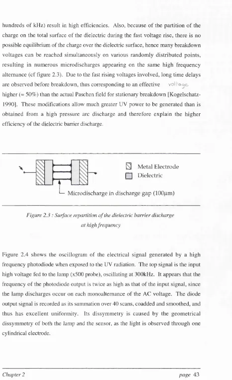
hundreds of kHz) result in high efficiencies. Also, because of the partition of the charge on the total surface of the dielectric during the fast voltage rise, there is no possible equilibrium of the charge over the dielectric surface, hence many breakdown voltages can be reached simultaneously on various randomly distributed points, resulting in numerous microdischarges appearing on the same high frequency alternance (cf figure 2.3). Due to the fast rising voltages involved, long time delays are observed before breakdown, thus corresponding to an effective v o l
higher (~ 50%) than the actual Paschen field for stationary breakdown [Kogelschatz- 1990]. These modifications allow much greater UV power to be generated than is obtained from a high pressure arc discharge and therefore explain the higher efficiency of the dielectric barrier discharge.
L
S Metal Electrode
nn Dielectric
Microdischarge in discharge gap (100pm)
Figure 2.3 : Surface repartition of the dielectric harrier discharge
at high frequency
Figure 2.4 shows the oscillogram of the electrical signal generated by a high frequency photodiode when exposed to the UV radiation. The top signal is the input high voltage fed to the lamp (x500 probe), oscillating at 300kHz. It appears that the frequency of the photodiode output is twice as high as that of the input signal, since the lamp discharges occur on each monoalternance of the AC voltage. The diode output signal is recorded as its summation over 40 scans, coadded and smoothed, and thus has excellent uniformity. Its dissymmetry is caused by the geometrical dissymmetry of both the lamp and the sensor, as the light is observed through one cylindrical electrode.
CH I 5V/DFV Input Signal
- CH2 5m V /D IV D iode Output
lus/D IV
CHI
CH2
Figure 2.4 : Oscillogram o f feeding voltage (upper trace), and photodiode output (X=172nm).
1.2.2- The pressure effect
3
1
172nm 146nm
0
130 140 150 160 170 180 190 200
500 mbar 150 mbar 80 mbar 30 mbar
Wavelength (nm)
Figure 2.5: Pressure dépendance in a xenon dielectric barrier discharge
(the spectra have been re-drawn from scanned records).
(Spectra obtained with the light source presented in § 3.3.1, figure 2.20).
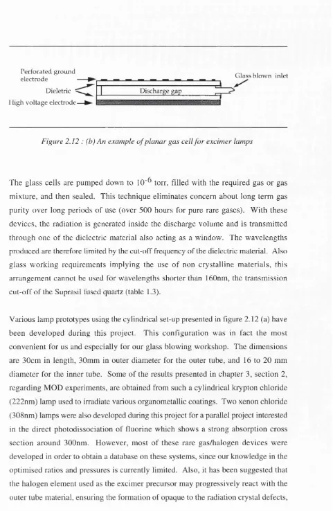
1.2.3- The excimer formation
This phenomenon was first explained by Forster and Kasper in terms of the formation of a complex containing two pyrene molecules [Forster]. The complex has been given the name “excimer” since it is a
dimer,
which is stable in an electronically excited state [Gilbert]. The existence of excimer generation stands in the absence of an electronically stable ground state.Excimer formation can be represented by
M*+M —> MM* (2.1)
where M is a ground state, M an excited state, and MM* the corresponding dimer.
To explain this process, reference is made to the following simplified energy diagram (figure 2.6).
Xe+Xe Xe+Xe' Xe+Xe
second
continuum atomic transition 172 nm
Xe + Xe
►
intemuclear req
separation
Figure 2.6 : Simplified band diagram for excimer generation


![Figure 2.14 : Spectral response (top) [Watanabe]](https://thumb-us.123doks.com/thumbv2/123dok_us/9135587.1449355/64.597.39.550.39.729/figure-spectral-response-top-watanabe.webp)