Analysis on Controlled Rectifier to Determine the
Minimum Limit of Load Resistance for Proper
Voltage Regulation
A. Mohammad, S. A. M. Shah Ul Amin, A. Mahmud, R. Ahmed, Md. Rokib Hasan, Al-Imran and Md. Ferdous
Abedin
Department of Electrical and Electronic Engineering American International University – Bangladesh (AIUB)
Dhaka, Bangladesh [email protected]
Abstract— Existence of source resistance plays a major
impact on the voltage regulation of a controlled rectifier. Based on the fact necessary mathematical equations have been derived to find out the minimum limit of electrical load resistance for which voltage regulation is only possible. Below that resistance, no control system can regulate the output voltage of the converter. In addition, it can be used to define the maximum power which will be crucial for designing a regulated power supply. Hence, to design a closed loop control system for voltage regulation this solution is useful.
Index Term-- controlled rectifier; voltage regulation; source resistance; regulated converter; voltage gain.
I. INTRODUCTION
Impact of source resistance on the performance of power electronic converter is a very important sphere of research [1]. Recent research on the impact of source resistance has been done to define the limit of load resistances for proper voltage regulation in dc to dc converter [1]. In this paper the impact of source resistance on the performance of controlled rectifier is the main focus of analysis to define the range of load resistance for proper voltage regulation.
Rectifiers are used to convert ac signal into dc signal [2-5]. Controlled ac/dc converters provide high reliability, low complexity, low power loss and minimize the numbers of series-connected switches for high-voltage or medium voltage applications [6-8]. The value of output voltage can be easily controlled in controlled rectifiers by varying the delay angle [9-14]. It is desired to get a fixed dc output voltage for changing loads. In ideal analysis of single phase controlled rectifier the effect of input source resistance and the voltage drop across the switch are ignored [9-14]. Practically, the source resistance exists. This paper analyzes the impact of source resistances on the performance of the converters excluding the voltage drop across the switch.
The mathematical analysis including the equivalent circuits at different states of switching is carried out in section II. A relationship between cosine of practical delay angle and ideal delay angle is shown in the section II. The end of section II reflects the range of delay angle and limit of change in load connected to the converter up to which voltage regulation is possible. Section III analyzes the characteristics of the
converters depending on the analysis of section II. The simulation is performed in MATLAB.
II. NECESSARY DERIVATIONS AND IMPACT ANALYSIS OF
SOURCE RESISTANCE
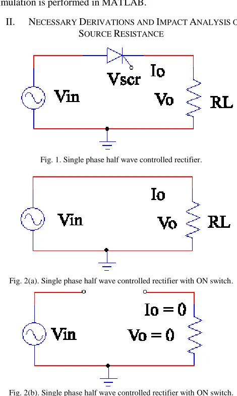
Fig. 1. Single phase half wave controlled rectifier.
Fig. 2(a). Single phase half wave controlled rectifier with ON switch.
Fig. 2(b). Single phase half wave controlled rectifier with ON switch.
2 ) cos Vm.(1
Vo(avg)
and no impact of source resistance. The average voltage of this converter is [9-14],
(1)
Where, Vm is the peak value of input sinusoidal wave and
is the delay angle (with respect to the origin or main reference point of the axes) at which gate pulse is provided to turn ON the SCR [9-14]. From (1) it is clear that, the output voltage is dependent on delay angle for a particular input voltage.
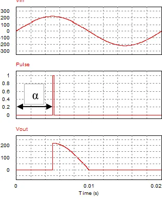
Fig. 3. Input voltage, gate pulse including delay angle and output voltage.
Fig. 3 shows the operation of the converter in terms of their wave shapes. A gate pulse is provided to turn ON the SCR. α is the delay angle. The higher the value of delay angle the lower will be the area covered by output voltage. The range of delay angle is 0 to π.
In practical cases, there will be source resistance and voltage drop across the switch. In this paper a small fixed voltage drop is considered throughout the analysis and it includes the existence of source resistance. Mainly, the performance of the converter will be analyzed to show the effect of input resistance.
Fig. 4 (a). Single phase half wave controlled rectifier including the effect of source resistance.
Fig. 4 (b). Single phase half wave controlled rectifier at ON switch state including the effect of source resistance and voltage drop across the switch.
Fig. 4 (c). Single phase half wave controlled rectifier at OFF switch state including the effect of source resistance.
Fig.4 shows the equivalent circuit of the converter considering the internal resistance of the source and small voltage drop across the switch for both ON and OFF states. At ON state current will flow from source to the load via source resistance and switch. At OFF state of switch there will be no current flow and the output voltage will be zero.
At ON state the output voltage of the converter,
(2) Where, Vin is input sinusoidal wave, Io is the output current, Rs is the input sourse resistance and Vscr is the ON state voltage drop across the SCR.
Using
RL Vo Io in (2),
(3)
From (3), it is visible that the output voltage is also dependent on the resistances (Rs) of voltage source and the load (RL). In ideal case the effect of source resistance and switch voltage drop are neglected. So, for ideal case Rs has a value of zero. In (3), RL is the load resistance.
Putting Rs=0 and Vscr =0 in (3),
(4) Where, is angular frequency of input and t is the time. Equation (4) matches with the ON state condition of ideal analysis (Fig. 2(a)).
At off state of the switch, the output voltage is zero. So, the average output voltage in a period of T and with a delay angle of α,
(5) Solving (5),
(6)
Vscr) (Io.Rs -Vin
Vo
RL Rs 1
Vscr -Vin Vo
t) Vm.Sin( Vin
Vo
2
t .d 1
Vscr -t) Vm.Sin(
Vo(avg)
0
RL
Rs
) .(1 2
) -Vscr.( -) Cos Vm.(1 Vo(avg)
RL Rs
2 ) cos( 1 VmVo(avg) i
2 ) ) cos( Vm.(1
Vo(avg) i
As indicated previously ignorance of Vscr and Rs will result the ideal equation of output voltage (1) from (6).
This is also clear that if the source resistance is not zero, then the output voltage becomes dependent on the variation of output or load resistance RL. If the source resistance is zero (ideal situation) then from (6),
(7)
Equation (7) shows no dependency of the average output voltage on the change of load resistance. In this situation the output voltage will remain same for any output resistance.
Suppose, the delay angle of ideal case is denoted by αi and αp for practical case, then from (1) and (6),
(8) (9) ) -.( Vm Vscr p
in (9) can be ignored because, Vscr<<Vm. So,
(9) can be expressed as,
(10)
From (8) and (10),
( (11)
Equation (11) shows the relation between ideal delay angle which helps to represent the range of practical converter and practical delay angle (α). More precisely it can be stated that, for all converters (ideal and practical) the range of delay angle is 0 to π.Whenever performance of any thing is analyzed it should be compared with a standard or ideal case. So, here the standard is the ideal converter and the performance of the practical converter is the issue of analysis.
From (11), it is clear that the Cos(αp) will be always greater than Cos(αi).
Range of α is from 0° to 180° [9-14]. From the given range of α, the range of Cosα becomes -1 to +1. From the above discussion some conditions can be stated for either lower limits of delay angles or upper limits of Cosα,
(a) Cos(αp)>Cos(αi)
(b) Upper limit for practical Cosα: Cos(αp) = 1 or, αp = 0 (c) Upper limit of ideal Cosα for which ideal gain
coincides with the maximum gain of practical converter: Cos(αi)<1 or, αi>0
Form the above conditions, lower limit of αi (upper limit of Cos(αi )) for which voltage gain of ideal converter coincides the maximum voltage gain of practical converter can be derived using Cos(αp)=1 in (11),
(12) Where, ill is the lower limit of ideal delay angle for which the voltage gain of ideal converter coincides with the maximum gain of practical converter. It means maximum gain of the practical converter will be smaller than the maximum gain of ideal converter. Using (12) in (8), the maximum gain for practical converter can be found from ideal converter.
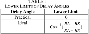
TABLEI
LOWER LIMITS OF DELAY ANGLES
Delay Angle Lower Limit
Practical 0 Ideal ) ( 1 RS RL RS RL Cos
Table I shows the lower limits of delay angles for ideal (which represents the practical converter) and practical cases. Upper limit of α or lower limit of Cosα can be found from (11) using Cos(αp) = -1,
(13)
TABLEII
UPPER LIMITS OF DELAY ANGLES
Delay Angle Upper Limit
Practical π
Ideal π
Table II shows the upper limit of delay angles. So, the limits for which delay angles for the practical and ideal cases coincide can be expressed as,
π≥ αp ≥0 (14)
and, π≥ αi ≥ 1( ) RS RL RS RL Cos (15)
Application of (14) in (10) and (15) in (8) will yield the same results.
2 ) -Vscr.( -) Cos Vm.(1 Vo(avg) ) .(1 2 ) -Vscr.( -)) Cos( Vm.(1 Vo(avg) RL Rs p p
) .(1 2 ) -.( Vm Vscr -) ) Cos( (1 Vm Vo(avg) RL Rs p p
) .(1 2 ) Cos( 1 2 )) cos( (1 RL Rs p i RL RS RL RS i Cos pCos( ) ().(1 )
0 0.5 1 1.5 2 2.5 3 3.5 0 0.1 0.2 0.3 0.4 Delay Angle V ol ta ge G ai n Ideal Converter
Practical Converter (RL=0.5 Ohm) Practical Converter (RL=0.2 Ohm) Practical Converter (RL=0.1 Ohm)
0 1 2 3 4 5
0 0.05 0.1 0.15 0.2 0.25 0.3 0.35
Loar Resistance (Ohm)
M axi m um V ol ta ge G ai n of P ra ct ic al C onv er te r TABLEIII
GAIN ANALYSIS OF THE CONVERTERS
Gain of Practical Converter Gain of Ideal Converter
Lower, α 0 Lower, α 0
Upper, α π Upper, α π
Maximum Gain ) .(1 1 RL Rs Maximum
Gain
1
Minimum Gain
0 Minimum
Gain
0
Relationship between the maximum gains of both cases can be derived using the results from Table III.
Maximum voltage gain of practical converter,
(16)
Where, Avp(max) is the maximum voltage gain of practical converter and Avi(max) is the maximum voltage gain of ideal converter which is 0.318. From (16), the previous discussions on the gains of converters become mathematically proved. The denominator term of (16) will always be greater than one. So the gain of practical converter will be smaller than ideal cases. If the source resistance is considered zero (ideal situation) in practical converter then both of the gains become equal.
An analysis for maximum load (minimum RL) for which voltage regulation is possible can be performed using maximum limit of Cos(αp) = 1 in (10),
(17)
For a specific voltage gain, if the value of RL becomes smaller than RLmin then the output voltage cannot be regulated at desired value. To justify the statement above an example can be provided using (10) and (17).
Suppose, output of a converter which has a source resistance of 0.2 Ω is desired to be 5 V for an input of 311 Vpeak (gain for this case is 0.0161). Using (17),
If the value of connected load (RL) becomes less than 0.0106 Ω then, the output voltage or the voltage gain cannot be maintained at desired value. Equation (10) can be used to justify this condition.
For a specific voltage gain, if the value of RL becomes smaller than RLmin then the output voltage cannot be regulated at desired value. To justify the statement above, an example can be provided using (10) and (17). Taking load of 0.005 Ω (less than the calculated value, 0.0106 Ω), the solution of (10) for source resistance of 0.2 Ω and voltage gain of 0.0161 becomes,
This is not valid, because maximum range of Cosα is +1 [9-14]. So, voltage gain or output voltage will not be at desired level rather it will be falling below the desired result.
III. NECESSARY SIMULATIONS
Fig. 5. Voltage gain and delay angle characteristics for the ideal and practical cases.
Fig. 5 shows the variation of voltage gain for different values of delay angles (radian). It depicts the gains of practical cases and compares among different practical cases which include different values of load resistances. The maximum gain for every load can be calculated using (10). In this analysis, the source resistance is taken as 0.2 Ω.
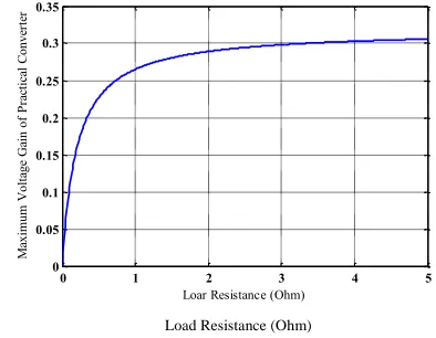
Fig. 6. Maximum voltage gain of practical converter for different load resistance.
Fig.6 is the graphical analysis of (16). It shows the maximum gains of practical converters for different load resistances. From the Fig. 6 and (16) it can be observed that if load resistance decreases (load or output current increases), then the voltage gain of practical converter starts to fall.
Fig. 7. Characteristics of cosine of ideal delay angle and practical case.
-1 -0.5 0 0.5 1
-1 -0.5 0 0.5
Cosine of Delay Angle of Practical Case
C os ine of D el ay A ngl e of I de al C as e
RL = 0.1 Ohm RL = 0.2 Ohm RL = 0.5 Ohm
RL Rs 1 Avi(max) = Avp(max) ) min .(1 1 Vm Vo(avg) RL Rs
.Vo(avg) -Vm Vo(avg).Rs . min
RL 0.0106 min RL 147 . 3 ) ( p CosFig. 7 shows the characteristics of cosine of the ideal delay angle and practical delay angle. This analysis is based on (11). It shows that, for lower values of RL (higher values of load) the steepness of characteristic becomes lower. Range of cosine is in between -1 to +1. From the Fig.7, it is clear that, for lower values of load resistance (higher values of load or current) the range of cosine of equivalent ideal angle becomes lower, it means range of voltage regulation or voltage gain regulation (which is obviously related with the delay angle according to (8) and (10)) for this case becomes smaller. In the case of higher values of load resistance (lower values of load), the range is higher and voltage regulation is more flexible for changing loads.
TABLEIV
RANGE ANALYSIS OF PRACTICAL CONVERTER RL Limits of Cosαi (Which
equivalently represents practical converter)
Range % Deviation
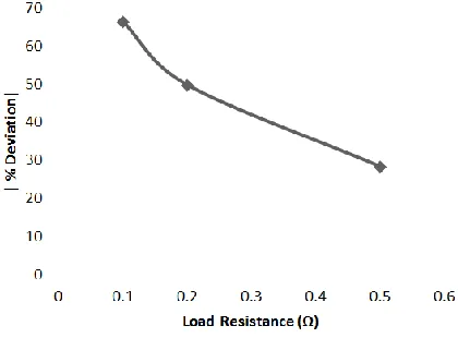
0.1 Ω -1 to -0.333 0.667 -66.665%
0.2 Ω -1 to 0 1 -50%
0.5 Ω -1 to 0.429 1.429 -28.55% Range of Cosα of Ideal Converter 2
Table IV shows the range of ideal converter for equivalent representation of the operating range of practical converter. It shows the range for which voltage regulation is possible. For ideal converter the limit of Cosα is -1 to +1. So, the range becomes 1-(- 1) = 2. The range of ideal converter is taken as standard to calculate percentage deviation of practical converter for different load resistances. It shows that, for lower values of load resistance the percentage deviation is higher. It means the practical converter with low resistance is more deviated from the operating range of ideal converter. The formula below is used to calculate the percentage deviation of the converters [15],
% 100 . ORI
ORP -ORI %Deviation
Where, ORI is the operating range of Cosα of ideal converter and ORP is the operating range of Cosα of practical converter in terms of ideal converter.
Fig. 8. Deviation in percentage for varying load resistance.
The result of percentage deviation (in modulus) for different load resistance is shown in Fig. 8. It depicts that, for
lower load resistance the percentage deviation is higher. For light load (higher load resistance) the error is reducing. So, final error analysis based on the derived equations has been provided.
IV. CONCLUSION
This research proposes a mathematical solution for determining the minimum load resistance for which voltage regulation is possible. Research considering the practical fact is useful to design a controller circuit, which controls the main converter circuit. Failure to sustain above the determined load resistance will result unregulated output of the converter. Hence, this idea can be very important to design dc power supply for different systems such as, battery charging and dc drives. Future work can be performed to design a closed loop controller circuit using this mathematical solution.
REFERENCES
[1] Mohammad, Adnan; Rahaman, Md.Shafieur; Rahman, Syed Khalid; Ahmed, Omar; Aziz, Ashique Ibni; Muntakim, Tahmid Ul, "Impact of source resistance on duty ratio and output voltage of a DC to DC step down converter," in 2015 IEEE International Conference on Electrical, Computer and Communication Technologies (ICECCT), vol. 1, no., pp.1-4, 5-7 March 2015.
[2] M. H. Rashid, “Diode Rectifiers,” in Power Electronics Circuits, Devices and Applications, 3rd ed. New Delhi, India: Prentice Hall, 2004, pp. 68-121.
[3] Dr. P.S. Bimbhra, “Dioide Circuits and Rectfiers,” in Power Electronics, 5th ed. Daryaganj, New Delhi, India: Khanna Publishers, 2012, pp. 50-131.
[4] Power Electronics Handbook, 3rd ed. Butterworth-Heinemann, Burlington, Massachusetts, 2011, pp. 139-168.
[5] G.K. Mithal, Dr. M. Gupta, “Rectifiers and Regulated Power Supplies,” in Industrial and Power Electronics, 19th ed. Delhi, India: Khanna Publishers, 2006, pp. 55-110.
[6] M. H. Hamad, M. I. Masoud, B. W. Williams, “Medium-Voltage 12-Pulse Converter: Output Voltage Harmonic Compensation Using a Series APF,” IEEE Trans. on Industrial Electronics, vol.61, no.1, pp. 43 – 52, Feb. 2013.
[7] N. Akagi, “Large static converters for industry and utlity applications,” Proc. IEEE, vol. 89, no. 6, pp. 976-983, Jun. 2001.
[8] B. K. Bose, Power Electronics and AC Drives. Englewood Cliffs, NJ, USA: Prentic-Hall, 1986.
[9] M. H. Rashid, “Controlled Rectifiers,” in Power Electronics Circuits, Devices and Applications, 3rd ed. New Delhi, India: Prentice Hall, 2004, pp. 431-499.
[10] S. Sivanagaraju, M. B. Reddy, A.M. Prasad, “Phase-Controlled Converters,” in Power Electronics, 1st ed. New Delhi, India : PHI Learning Private Limited, 2010, pp. 123-168.
[11] Dr. B.R. Gupta, V. Singhal. “Controlled Rectifiers,” in Power Electronics, 6th ed. Delhi, India: S.K. Kataria & Sons, 2010, pp. 125-198.
[12] Dr. P.S. Bimbhra, “Phase Controlled Rectfiers,” in Power Electronics, 5th ed. Daryaganj, New Delhi, India: Khanna Publishers, 2012, pp. 272-379.
[13] Power Electronics Handbook, 3rd ed. Butterworth-Heinemann, Burlington, Massachusetts, 2011, pp. 169-182.
[14] G.K. Mithal, Dr. M. Gupta, “Thyristor Converters,” in Industrial and Power Electronics, 19th ed. Delhi, India: Khanna Publishers, 2006, pp. 215-231.
Adnan Mohammad is working as a lecturer in the department of electrical and electronic engineering in American international university - Bangladesh (AIUB) since January, 2013. Before that, he started his teaching career from Eastern University, Bangladesh. Currently, He is continuing his M.Sc. in Bangladesh University of Engineering and Technology (BUET). He has done several research works on power electronics and drive system. Many undergraduate thesis works are supervised by him.
S. A. M. Shah Ul Amin has graduated from American
International University – Bangladesh (AIUB). Currently, besides his job, he has involved himself in the research. His research interests include power electronics and telecommunications.
Abdullah Mahmud is currently completing the Bachelor
of Science Degree in Electrical and Electronic Engineering at American International University-Bangladesh. A strong advocate of hands on, theoretical and practical based learning, he involves his studies in doing numbers of project and thesis based works on robotics, mathematical modeling, programming and power engineering. His academic interests focus on power electronics and robotics related projects and his current projects include control of voltage source inverter using PWM and microcontroller based humanoid walking robot.
Rakib Ahmed has received B.Sc. in Electrical and
Electronic Engineering degree from American International University-Bangladesh (AIUB) in 2016. His area of research interests are power electronics, power system & generation and renewable energy.
Md. Rokib Hasan has completed B. Sc. in Electrical and
Electronics Engineering from American International University Bangladesh (AIUB). He is interested in nano-electronics, power electronics and embedded system.
Al-Imran has earned B. Sc. in Electrical and Electronics
Engineering from American International University-Bangladesh. He finds his research interests in communication and electronics.
Md. Ferdous Abedin has graduated from American