IJIRT 147184
INTERNATIONAL JO URNAL OF INNOVATIVE RESEARCH IN TECHNOLOGY170
Implementation of Fast Counting L2 Cache Architecture
Using Bloom Filter
S. Sathyadeepa
1, T. Sasikala
2, B. Suresh
31
Assistant Professor, Department of Electronics, Hindusthan College of Arts and Science, Coimbatore
2& 3
Department of Electronics and Communication Systems, VLB Janakiammal College of Arts and
Science, Coimbatore
Abstract- Many high-performance microprocessors employ cache write-through policy for performance improvement. However, write-through policy also incurs large energy overhead due to the increased accesses to caches at the L2 caches. To overcome this problem we use way tagged cache. In the exiting work, we present novel ideas for both cache hit and miss predictions. Partial tag enhanced bloom filter to reduce the tag comparisons of the cache hit prediction method. In the proposed technique enables CBFs(counting bloom filters)to improve upon the energy, delay, and complexity of various processor structure when compared with exiting work. This paper studies the energy, delay, and area characteristics of two implementations for CBFs using full custom layouts in a commercial 0.13- m fabrication technology. One implementation is S -CBF, other implementation is CBF. Our results demonstrate that for a variety of L-CBF organizations, the estimations by analytical models are within 5% and 10% of spectra simulation results.
Index Terms- Computer architecture, counting bloom
filters, Implementation, low power, microprocessors.
INTRODUCTION
Multi-Level on-chip cache systems have been widely adopted in high-performance microprocessors. To keep data consistence throughout the memory hierarchy, write-through and write-back policies are commonly employed. Under the write- back policy, a modified cache block is copied back to its corresponding lower level cache only when the block is about to be replaced. While under the write-through policy, all copies of a cache block are updated immediately after the cache block is modified at the current cache, even though the block might not be evicted. As a result, the write-through policy maintains identical data copies at all levels of the cache hierarchy throughout most of their life time
of execution. This feature is important as CMOS technology is scaled into the nanometre range, where soft errors have emerged as a major reliability issue in on-chip cache systems. While enabling better tolerance to soft errors, the write-through policy also incurs large energy overhead. This is because under the write-through policy, caches at the lower level experience more accesses during write operations. Consider a two-level (i.e., Level-1 and Level-2) cache system for example. If the L1 data cache implements the write-back policy, a write hit in the L1 cache does not need to access the L2 cache. In contrast, if the L1 cache is write-through, then both L1 and L2 caches need to be accessed for every write operation. Obviously, the write-through policy incurs more write accesses in the L2 cache, which in turn increases the energy consumption of the cache system. Power dissipation is now considered as one of the critical issues in cache design. Studies have shown that on-chip caches can consume about 50%
of the total power in high-performance
microprocessors.
The way-tagged cache, to improve the energy efficiency of write-through cache systems with
minimal area overhead and no performance
degradation.
Several studies have investigated the reduction of tag comparisons within the L2 cache. Such studies can be classified into two categories based on the method used for reducing tag comparisons: cache hit prediction and cache miss prediction.
IJIRT 147184
INTERNATIONAL JO URNAL OF INNOVATIVE RESEARCH IN TECHNOLOGY171
prediction fails, tag comparisons with the remaining tags are performed in the next cycle, thereby resulting in an additional latency cycle. Because tag comparisons are performed even in the case of cache misses, the cache hit prediction methods may lead to high power consumption in applications with high cache miss rates.
The cache miss prediction methods try to predict cache misses, e.g., based on the Bloom filter . If the prediction is correct, tag comparisons are skipped, thereby saving the energy consumed in tag comparison. Improving the prediction accuracy (e.g., by using a larger Bloom filter) further reduces the amount of energy consumed in tag comparison. In this paper, we propose a novel tag comparison method that exploits predictions of both cache hits and misses.
The contributions of our work are as follows:
1) A partial tag-enhanced Bloom filter to improve
the energy efficiency of cache miss predictions;
2) Hot/cold checks to improve the efficiency of
cache hit prediction with energy-aware dynamic management of the hot/cold data and a pessimistic two-step tag comparison for cold data;
3) Dynamic reordering of cache hit/miss prediction
methods for multistep tag comparison that can further reduce the energy consumed in tag comparison by adapting to dynamically changing cache access behavior;
4) Performance guarantees to ensure a tradeoff
between cache energy consumption and
additional latency overhead, especially in the case of latency-critical programs.
This work focuses exclusively on the second factor as it investigates implementations of a CBF that improve its energy and delay characteristics. A key contribution of this work is the introduction of L-CBF. L-CBF is an energy- and delay-efficient implementation that utilizes an array of up/down linear feedbackshift registers (LFSRs) and local zero detectors. Previous work assumes a straightforward SRAM-based implementation that we will refer to it as S-CBF.
The significant contributions of this work are as follows.
1) It proposes L-CBF, a novel, energy- and
speed-efficient implementation for CBFs.
2) It compares the energy, delay, and area of two
CBF implementations, L-CBF and S-CBF, using
3) their circuit-level implementations and
full-custom layouts in 0.13- m fabrication
technology.
4) It presents analytical delay and energy models
for L-CBF and compares the model estimations against simulation results.
II. PRELIMINARIES AND OUR MOTIVATIONS
A. Bloom Filter
The Bloom filter is utilized to check the approximate non-member ship of a set. When applied to reducing tag comparisons, each cache way is equipped with a Bloom filter. A query to the Bloom filter (e.g., “is address 0×100 in the cache way?”) gives either of two results: negative (definite nonexistence) and positive (likely existence). Note that a negative result from the Bloom filter guarantees nonexistence,i.e., a cache way miss.
Preliminaries and Our Motivations cache way is accessed, first the Bloom filter per cache way is looked up. If the Bloom filter indicates nonexistence, then tag comparison for the cache way is avoided, thereby saving the energy that would have been consumed in tag comparison. Both: 1) the smaller energy consumed to access the Bloom filter rather than the tag; and
2) the high prediction accuracy
for cache way misses reduce the energy consumed in tag comparison. For instance, in the case of a cache way miss, using the Bloom filter produces a net energy gain as long as the following relationship holds
EB < p×ET
WhereEB and ET represent the energy consumed while accessing the Bloom filter and the tag structure, respectively, and pis the cache miss prediction accuracy of the Bloom filter.
III. CBFS
IJIRT 147184
INTERNATIONAL JO URNAL OF INNOVATIVE RESEARCH IN TECHNOLOGY172
Fig. 1. CBF as a black box A. Introduction to CBFs:
1) CBF as a Black Box:As shown in Fig. 1, a CBF is conceptually an array of counts indexed via a hash function of the element under membership test. A CBF has three operations:1) Increment count (INC); 2) Decrement count (DEC); and
3) Test if the count is zero (PROBE). The first two operations increment or decrement the corresponding count by one, and the third one checks if the count is zero and returns true or false (single-bit output). We will refer to the first two operations as updates and to the third one as a probe. A CBF is characterized by its number of entries and the width of the count per entry.
2) CBF Characteristics: Membership tests using CBFs are performed by probe operations. In response to a membership test, a CBF provides one of the following two answers: 1) “definite no,” indicating that the element is definitely not a member of the large set and
2) “I don’t know,” implying that the CBF cannot assist in a membership test, and the large set must be searched. The CBF is capable of producing the desired answer to a membership test much faster and saves power on two conditions. First, accessing the CBF is significantly faster and requires much less energy than accessing the large set. Second, most membership tests are serviced by the CBF. The latter is investigated by studying the application behavior. For instance, when CBF is exploited as a miss predictor, previous work shows that more than 95% of the accesses to the cache tag array are serviced by the CBF.
The CBF uses an imprecise representation of the large set to be searched. Ideally, in the CBF, a separate entry would exist for every element of the set. In this case, the CBF would be capable of precisely representing any set. However, this would require a prohibitively large array negating any benefits. In practice, the CBF is a small array and the element addresses are hashed onto this small array.
Because of hashing, multiple addresses may map onto the same array entry.
Hence, the CBF constitutes an imprecise
representation of the content of the large set and keeps a superset of the existing elements. This impreciseness is the reason of the “I don’t know” answers by the CBF. To reduce the frequency of such answers, and hence improving accuracy, multiple CBFs with different hash functions can be used.
Fig. 2. S-CBF architecture: an SRAM holds the CBF counts; INC/DEC: read modify-write sequences; PROBE: read-compare sequence.
An “I don’t know” answer to a membership test incurs power and delay penalty since in case of such an answer, the large set must be checked in addition to the CBF. The delay penalty occurs if the CBF and the large set accesses are serialized. This delay penalty can be avoided if we probe the CBF and the large set in parallel; in this case, power benefits will be possible only if the in-progress access to the large set can be terminated once the CBF prov ides a definite answer. These overheads do not concern us as often CBF can provide the definite answer. 3) CBF Functionality: The CBF operates as follows. Initially, all counts are set to zero and the large set is empty. When an element is inserted into, or deleted from the large set, the corresponding CBF count is incremented or decremented by one.
To test whether an element currently exists in the large set, the corresponding CBF count is inspected. If the count is zero, the element is definitely not in the large set; otherwise, CBF cannot assist and the large set must be searched.
IJIRT 147184
INTERNATIONAL JO URNAL OF INNOVATIVE RESEARCH IN TECHNOLOGY173
controller [2]. We will refer to this implementation as S-CBF. The architecture of S-CBF is depicted in Fig. 2.
Updates are implemented as read-modify-write sequences as follows:
1) The count is read from the SRAM; 2) It is adjusted using the counter; and 3)It is written back to the SRAM. The probe operation is implemented as a read from the SRAM, and a compare with zero using the zero-comparator. A small controller coordinates this sequence of actions. An optimization was proposed to speedup probe operations and to reduce their power. Specifically, an extra bit Z is added to each count. When the count is nonzero the Z is set to false and when the count is zero, the Z is set to true. Probes can now simply inspect.The Z bits can be implemented as a separate SRAM structure which is faster and requires much less power. This type of optimization iscompatible with bothS-CBF and L-CBF architectures.
IV. L-CBF: A NOVEL LFS BASED CBF IMPLEMENTATION
Demonstrates quantitatively that much of the energy in S-CBF is consumed on the SRAM’s bit lines and word lines. Additionally, in S-CBF, both delay and energy suffer as updates require two SRAM accesses per operation.
The shared counter may increase the energy and the delay further.
We could avoid accesses over long bit lines by building an array of up/down counters with local zero detectors. In this way, CBF operations would be localized and there would be no need to read/write values over long bit lines. L-CBF is such a design. For the CBF, the actual count values are not important and we only care whether a count is “zero” or “nonzero” .Hence, any counter that provides a deterministic up/down sequence can be a choice of counter for the CBF.
L-CBF consists of an array of up/down LFSRs with embedded zero detectors. L-CBF employs up/down LFSRs that offer a better delay, power, and complexity trade off than other synchronous up/down counters with the same count sequence length .As demonstrates,
L-CBF significantly reduces energy and delay compared to S-CBF at the cost of more area. The
increase in area though is a minor concern in modern processor designs given the abundance of on-chip resources and the very small area of the CBF compared to most other processor structures(e.g., caches and branch predictors).The rest of this section reviews up/down (reversible) LFSRs and discusses the architecture of L-CBF.
A. LFSRs
A maximum-length -bit LFSR sequences through
2n-1states. It goes through all possible code
permutations except one. The LFSR cons ists of a shift register and a few embedded XNOR gates fed by a feedback loop. Each LFSR has the following defining parameters:
width, or size, of the LFSR (it is equal to the
number of bits in the shift register);
number and positions of taps (taps are special
locations in
the LFSR that have a connection with the
feedback loop);
initial state of the LFSR which can be any value
except one (all ones for XNOR feedback). Without the loss of generality, we restrict our attention to the Galois implementation of LFSRs. State transitions proceed as follows. The non-tapped bits are shifted from the previous position. The tapped bits are XNORed with the feedback loop before being shifted to the next position. The combination of the taps and their locations can be represented by a polynomial.
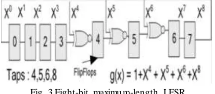
Fig. 3 shows an 8-bit maximum-length GaloisLFSR, its taps, and polynomial. By appropriately selecting the tap locations it is always possible to build a maximum-length LFSR of any width with either two or four taps. Additionally, ignoring wire length delays and the fan-out of the feedback path, the delays of the maximum-length LFSR is independent of its width (size) .Delay increases only slightly with size, primarily due to increased capacitance on the control lines.
IJIRT 147184
INTERNATIONAL JO URNAL OF INNOVATIVE RESEARCH IN TECHNOLOGY174
Fig. 4. Three-bit maximu m-length up/down LFSR. 1) Up/Down LFSRs:
The tap locations for a maximum-length,
unidirectional n -bit LFSR can be represented by a primitive polynomial g(x) as depicted in (1)
g(x)=∑ni=0Ci ×Xi(C0=Cn=1)---(1)
In (1),Xi corresponds to the output of theith bit of the shift register and the constants Ci are either 0 (no tap) or 1 (tap).
Given g(x), a primitive polynomial h(x) for an LFSR generates the reverse sequence as depicted in (2) h(x)= ∑ni=0Ci ×X n-i(C0=Cn=1)---(2)
The superposition of the two LFSRs (the original and its reverse) forms a reversible “up/down” LFSR. The up/down LFSR consists of a shift register similar to the one used for the unidirectional lLFSR; a 2-to-1 multiplexer per bit to control the shift direction; and twice as many XNOR gates as the unidirectional LFSR. Fig. 4 shows the construction of a 3-bit maximum-length up/down LFSR. It also depicts the polynomials and count sequence of both up and down directions. In general, it is possible to construct a maximum-length up/down LFSR of any width with two or six XNOR gates (i.e., four or eight taps. 2) Comparison With Other Up/Down Counters: In this section, we compare LFSR counters with other synchronous up/down counters that could be a choice of counter for CBFs. We restrict our discussion to synchronous up/down counters of Width n with a count sequence of at least 2n-1states.The simplest type of synchronous counter is the binary Modulo- 2nn -bit counter. For this counter, speed and area are conflicting qualities due to carry propagation. For example, the -bit ripple-carry synchronous counter, one of the simplest counters, has a delay of O(n). Counters with a Manchester carry-chain, carry-look ahead and binary tree carry propagation have delay of
O(log n) though at the cost of more energy and area. In applications where the count sequence is unimportant [e.g., ointers of circular first-inputs– first-outputs (FIFOs) and frequency dividers], an LFSR counter offers a speed-power-area efficient solution. The delay of an LFSR is nearly independent of its size. Specifically, the LFSR delay consists of a flip-flop delay, an XNOR gate delay, and a feedback loop delay. The feedback loop delay is the propagation delay of the last flip-flop output to the input of the furthest XNOR gate from the last flip-flop. Ignoring secondary effects on the feedback path, the delay of an n-bit maximum length LFSRis O(1) and independent of the counter size . These characteristics make LFSRs a suitable counter choice for CBFs.
B. L-CBF Implementation
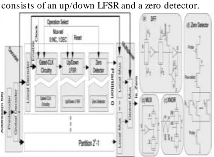
Fig. 5 depicts the high-level organization of L-CBF. L-CBF includes a hierarchical decoder and a hierarchical output multiplexer.
The core of the design is an array of up/down LFSR sand zero detectors. The L-CBF design is divided into several partitions where each row of a partition consists of an up/down LFSR and a zero detector.
IJIRT 147184
INTERNATIONAL JO URNAL OF INNOVATIVE RESEARCH IN TECHNOLOGY175
The decoder consistsof a predecoding stage, a global decoder to select the appropriate partition, and a set of local decoders, one per partition.
Each partition has a shared local is-zero output. A hierarchical Multiplexer collects the local is -zero signals and provides the single-bit is-zero output. Fig. 5 also depicts the basic cells of each up/down LFSR and zero decoder. Shown are the flip-flop used in the shift registers, the multiplexer that controls the direction of change (“up”/”down”), the XNOR gate, and a bit-slice of the zero decoder. Further details on L-CBF implementation are presented.
Multi-Porting: Some applications require
simultaneous operations from the CBF. In the simplest implementation, the CBF can be banked to support simultaneous accesses to different banks. This mirrors the organization of high-performance caches that are often banked to support multiple accesses instead of being truly multi-ported. True multi-porting is straightforward by selective resource replication in case of simultaneous accesses to different counts.
For S-CBF, we need an SRAM with multiple read and write ports and multiple shared up/down counters.
For L-CBF, we need to replicate the decoder, the zero detectors, and the output multiplexer.
When multiple accesses map to the same count, multi-portingis not straightforward. A simple solution
detects such accesses and serializes them.
Alternatively, circuitry can be added to determine the collective effect of all accesses. For example, for two simultaneous increment operations , the net effect is to increase the counter by two. For S-CBF, this circuitry can be embedded into the shared counter. For L-CBF, the capability of shifting by multiple cells in one cycle is required. This work does not consider these enhancements.
V. EXPERIM ENTA L RESULTS
This section compares the energy, delay, and area of S-CBF and L-CBF. Moreover, this section compares the analytical model estimations against simulation results for L-CBF. We compare S-CBF and L-CBF on a per operation basis.
Both designs are implemented using the Cadence(R) tool set in a commercial 0.13- m fabrication
technology. We developed transistor-level
implementation and a full-custom layout for both designs that were optimized for the energy -delay product.
We employed Spectre for circuit simulations. This is a vendor recommended simulator for design validation prior to manufacturing.
The rest of this section is organized as follows. We initially consider a 1 K-entry CBF with 15-bit counts as this configuration is representative of the CBFs used in previous proposals. Then, we present results for other CBF configurations.
We compare the energy, delay and area of the two designs for all CBF operations (updates and probes). We study how energy and delay change as the number of entries and the width of the counters vary. In Section V-C, we discuss the accuracy of analytical models.
A. Delay and Energy Per Operation
We compare implementations of a 1 K-entry, 15-bit count per entry CBF. For S-CBF, an SRAM with a total capacity of15 Kbits is used.
The SRAM is partitioned to minimize the energy -delay product. For S-CBF, we do not consider the delay and energy overhead of the shared counter since our goal is to demonstrate that L-CBF consumes less energy and is also faster.
To further reduce energy for probes in S-CBF, we introduce an extra bit per entry which is updated only when the count changes from, or to, zero. On a probe, we only read this bit. Furthermore, we apply a number of delay and power optimizations on S-CBF. In detail, we implement the divided word line (DWL) technique which adopts a two-stage hierarchical row decoder structure.
The DWL technique improves speed and power. Moreover, we reduce power further via pulse operation techniques for the word-lines, the periphery circuits and the sense amplifiers. We also use multistage static CMOS dedecoding
and current-mode read and write operations to further reduce power [12]. For L-CBF, we utilize 16-bit LFSRs such that the LFSR can count at least 215 values.
IJIRT 147184
INTERNATIONAL JO URNAL OF INNOVATIVE RESEARCH IN TECHNOLOGY176
respectively, measurements for the update and probe operations.
TABLE II ENERGY, DELAY, AND AREA OF S-CBF AND L-S-CBF IMPLEMENTATIONS FOR A 1 K-ENTRY, 15-BIT CBF
operation L-CBF S-CBF
S-CBF/L -CBF
Delay(ps) INC/DEC 447.26 1670 3.7
PROBE 580.32 910.12 1.6
Energy(pj) INC/DEC 38.73 88.98 2.3
PROBE 30.36 41.02 1.4
Area(mm2)
0.95 0.30 0.31
For delay and energy, we report the worst case which is measured by selecting appropriate inputs. The delay and energy of the shared counter of S-CBF is not included; otherwise, the actual delay and energy of S-CBF would be higher.
As observed from Table II, L-CBF is 3.7 and 1.6 faster than S-CBF during update and probe
operations, respectively. In addition, L-CBF
consumes 2.3 or 1.4 X less energy than S-CBF for update and probe operations, respectively. These significant gains in speed and energy consumption come at the expense of more area. L-CBF requires about 3.2 more area than S-CBF.
Area is less of a concern in modern microprocessor designs.
Disregarding the overhead (delay and energy) of the shared counter, the measurements for S-CBF are optimistic. Anup/down 15-bit LFSR counter has a delay of 240 ps and energy per update of 25 FJ. If this LFSR was used as the shared counter for S-CBF, L-CBF would be 4.3 or 1.98 X faster than S-CBF.
VI. CONCLUSION
In this paper, we investigate physical level implementations of CBFs and we propose CBF. L-CBF is a novel implementation consisting of an array of up/down LFSRs and zero detectors.
We compare L-CBF with S-CBF. S-CBF is the previously assumed implementation consisting of an SRAM array of counts and a shared counter. We evaluate the energy, delay, and area of L-CBF and S-CBF in a commercial fabrication technology. L-S-CBF is superior to S-CBF in both delay and speed at the expense of more area.