Analysis of Multiphase Boost Converter for High
Power Application
Dinesh K
Assistant professor,
Kanchi Pallavan Engineering
College. Kanchipuram
TamilNadu, India
ABSTRACT
In this paper, a multiphase boost converter is proposed to achieve high voltage gain and high power gain. The proposed converter operates in continuous conduction mode (CCM) with soft switching of main and auxiliary devices. The transformer in a conventional converter is replaced by an auxiliary circuit which provides the desired voltage and power levels. The zero voltage switching (ZVS) and zero current switching (ZCS) of the devices is achieved in this topology. The proposed converter is configured with proper number of series and parallel connected basic cells in order to obtain the required output voltage and power levels respectively. Simulation results are presented for a 380V, 750W and 230V, 3000W loads.
General Terms
Boost converter, analysis of duty cycle, key wave forms
Keywords
High power applications, multiphase conversion, non-isolated converter, soft switching
1.
INTRODUCTION
Continuous conduction mode boost converters are increasingly needed in high power applications such as hybrid electric vehicles, fuel cell conversion systems and UPS [1], [2]. The hard switched CCM boost converter suffers from severe diode reverse recovery problem in high current high power applications. The quasi-resonant converter (QRC) achieves both zero voltage switching of main switching and zero current switching of diodes. Due to resonant operation excessive voltage stress is occurred. To reduce the voltage stress many soft switching techniques on CCM boost converters have been proposed in [3]-[7]. Isolated boost converters are very desirable for low-to-high voltage conversion. The low-to-high voltage conversion requires the isolated boost converter to sustain the high current at the input and high voltage at the output. If two or more isolated CCM boost converter cells are parallel connected at the input and series connected at the output both the current stress and voltage stresses of the transformer and switches of the converter can be reduced into half [8]-[10]. The converter is controlled by interleaved method which has the same switching frequency and same phase shift. By operating the converter in high frequency the size and losses of the filtering stages could be reduced [9]. As power level increase, input currents quickly reach levels where paralleling of primary switches become necessary. Since transistors are often operated close to maximum drain current rating, direct paralleling of MOSFET’s may require screening a parameter
matching of on-resistance, gain and/or threshold voltage [11]. Multiphase DC-DC converter is configured in such a way that the boost half bridge (BHB) cell and the voltage doubler rectifier are connected in series, parallel or combination of them at the primary and secondary respectively, to increase the output voltage and/or the output power [12]. In multiphase boost converter the transformer is replaced by an auxiliary circuit, to increase the voltage as well as power respectively. This paper proposes a new multiphase boost converter suitable for high power applications such as hybrid electric vehicles, fuel cell conversion systems and UPS. The proposed converter has the following features: soft switching of power switch and diodes are achieved, negligible diode reverse recovery due to ZCS turn-off of the diode, voltage conversion ratio is five times improved compared to the classical boost converter, high step-up voltage and high power is achieved by paralleling the converter with basic cells.
2.
MULTIPHASE BOOST CONVERTER
2.1
Generalized multiphase DC-DC
converter
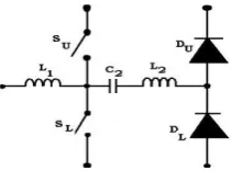
Fig.1 shows a basic cell which is used as a building block to build the proposed multiphase boost converter. The basic cell consists of an input filter inductor, a switch leg and diode leg, and an auxiliary inductor and capacitor. Fig. 2 shows the generalized circuit of the proposed multiphase DC-DC converter. The generalized converter has “N” groups of converters, where each group of switch legs is connected in parallel at the low-voltage high-current side, while output capacitors in each group is connected in series at the high-voltage low current side. Each of the N groups also has “P” parallel connected switch legs to increase the output power, where “P” is the number of switch or diode legs connected to the same output capacitor. Thus, “N” could be increased to get higher output voltage and “P” could be increased to get higher output power.
Fig 2: Generalized topology of multiphase boost converter
2.2
Soft switched boost converter
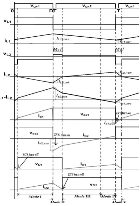
Fig. 3 shows the circuit diagram of the soft switched CCM boost converter, Fig. 4 shows key waveforms illustrating the operation of the proposed converter.
Fig 3: Basic circuit of soft switched Boost converter
Upper switch S2 in soft switched boost converter replaces the
rectifier diode in the conventional boost converter. Lower switch S1 and upper switch S2 are operated with asymmetrical
switching to regulate the output voltage as shown in Fig. 4. An auxiliary circuit that consists of a capacitor C1, an inductor
L2, two diodes D1 and D2, and a capacitor C2 is connected on
top of the output capacitor C3 to form the output voltage of the
converter. The auxiliary circuit not only increases the output voltage, but also helps ZVS turn-on of active switches S1 and
S2 in CCM.
2.3
Operating Principle
As shown in Fig.4, the operation of the soft switched boost converter can be divided into five modes. The equivalent circuits for each mode are shown in Fig. 5.
Mode I: This mode begins when iL2 decreases to zero and D2
is turned on as shown in the Fig. 4. During this mode, the lower switch S1 maintains ON state. Both input inductor
current iL1 and auxiliary inductor current iL2 flows through
lower switch S1. The slope of these currents are given by
,
di
L1dt
=
V
iL
1(1)
di
L2dt
=
(V
C1− V
C3)
L
2(2)
Mode II: This mode begins when S1 is turned off and the
body diode of S2 is turned on. The gating signal for
S
2is
applied during this mode, and S2 is turned on under ZVS
conditions. Both iL1 and iL2 are decreasing with the slope
determined by the following equations:
di
L1dt
=
(V
i− V
C3)
L
1(3)
di
L2dt
=
V
C1L
2(4)
At the end of this mode, inductor current iL2 changes its
direction of flow and D1 starts to conduct. It should be noted
that D2 is turned off under ZCS.
Mode III: during this mode, iL1, keeps decreasing with the
slope determined in mode II, and iL2 increases with slope
determined by the following equations:
di
L2dt
=
(V
C1− V
C2)
L
2(5)
At the end of this mode, switch current iS2 reverses its
direction of flow and conducts the main channel of S2. Mode IV: During this mode, iL1 and iL2 keep flowing with
the same slope determined in mode III.
Mode V: This mode begins when S2 is turned off and the
body diode of S1 is turned on. The gating signal for S1 is
applied during this mode, and S1 could be turned on under
ZVS conditions. Inductor currents iL1 and iL2 start to increase
and decrease, respectively, with the slope determined by the following equation:
di
L1dt
=
V
iL
1(6)
di
L2dt
=
(V
C1− V
C2− V
C3)
L
2(7)
This state ends when the decreasing current iL2 reaches to 0V.
This is the end of one complete cycle. Note that diode D1 is
also turned off under ZCS
.
2.4
Voltage conversion ratio
To obtain the voltage gain of the proposed converter, it is assumed that the voltage across C1, C2, and C3are constant
during the switching period of TS. The output voltage is given
by
V
o= V
C2+ V
C3(8)
V
o=
V
i1 − D
eff(9)
Where the effective duty Deff is defined by
D
eff= D + M
1− M
2(10)
The output voltage can also be expressed asV
o=
2
Fig 4: key waveform of soft switched boost converter
where ΔV is the voltage drop caused by the duty loss (M2
-M1). From (9) to (11), the voltage drop ΔV can be obtained by
ΔV =
2V
i(M
2− M
1)
1 − D (1 − D + M
2− M
1)
(12)
According to volt-sec balance principle on L2, capacitorvoltage VC1 can be obtained by
V
C1= V
C2(1 − D − M
2− M
1+ DV
C3(13)
where V
C2and V
C3can be expressed as
V
C2=
(1 − D)
1
V
i(14)
V
C2=
(1 − D)
1
V
i− ΔV (15)
2.5
Design Specification
The values of L1 and L2 have to be found out such that the
following conditions should be satisfied, 1
2(L1IL1,max2 + L2IL2,−pk2 ) > 1
2(Cos 1+ Cos 1)( Vi
1 − D)2 (16)
1
2(L1IL1,+pk2 − L2IL1,min2 ) > 1
2(Cos 1+ Cos 1)( Vi
1 − D)2(17)
The value of L2 should be small to obtain soft switching.
Assuming a small value of L2 (say 4µH) by using equation
(17) the value of L1 is computed, where Cos1+Cos2 = 1.8nF.
Fig 5: Operation modes of the soft switched boost converter
The minimum inductor current is given as,
IL
1,min= I
o− ΔI (18)
𝐼𝐿
1,𝑚𝑎𝑥= I
o+ ∆ (19)
Where,
I
O=
P
o3.
MULTIPHASE BOOST CONVERTER
FOR HIGH POWER APPLICATIONS
3.1 Multiphase boost converter time period
for various duty cycles
A four leg multiphase boost converter with the following specifications is shown in Fig.6, Po = 1.86kW,2.6kW, 4.1kW, 6kW Vo = 193, 230,285, 342V, Vi = 42V, L1 = 50µH, L2=5µH, C1 and C2 = 10µF, C3, C4 and C5 = 220µF, fs=50kHz. This converter can be used to increase the power as well as voltage gain. The gain of the converter is given by the expression
,
𝐕
𝐨=
𝐍 + 𝟏
(𝟏 − 𝐃
𝐞𝐟𝐟)𝐕
𝐢(𝟐𝟏)
A voltage gain of about more than 5 is achieved compared to conventional boost converter. The circuit is simulated for the time period of 25ms at the load of 20Ω resistor. The soft switching conditions are also achieved in this converter. This converter is suitable for the high voltage dc drive applications. Due to the non-isolation, the device voltage and current stress is reduced compared to hard switched topologies. In this circuit the various values of duty cycles is analyzed for various voltage and power levels.The circuit operation and key waveforms presented in section II(c) is valid for the proposed four leg multiphase boost converter. To get a voltage, “P” and “N” were chosen to be 1 and 2 respectively.
3.2 Simulation results (0.4 duty)
The four leg multiphase boost converter with the specifications as mentioned in the section 3.1 was simulated using PSpice 9.2.
Fig 6: Multiphase boost converter with P = 2 and N = 2.
The controllable switches in the converter are implemented with IRF541 (100V, 27A, 0.085Ω) MOSFET. Fast recovery diodes MUR820 (600V, 8A) are used for diodes D1 to D8. Zero voltage turn-on was achieved for main and auxiliary switch. The diodes were operated under zero current turn-off conditions. The output voltage and power waveforms obtained from simulation show that the converter performance is satisfactory.
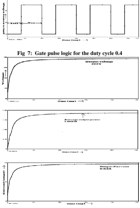
Fig. 7 shows the gate pulse waveforms for the main and auxiliary devices. For the one complete cycle, the total time Ton+Toff = 20µs.
Fig 7: Gate pulse logic for the duty cycle 0.4
Fig 8: Output Voltage, power and current waveforms
Fig. 8 shows the output voltage, current and power waveforms. It is observed that the converter fulfills the voltage and power requirement. The gain of the converter is improved almost 4.5 times and power of 1.86kW.
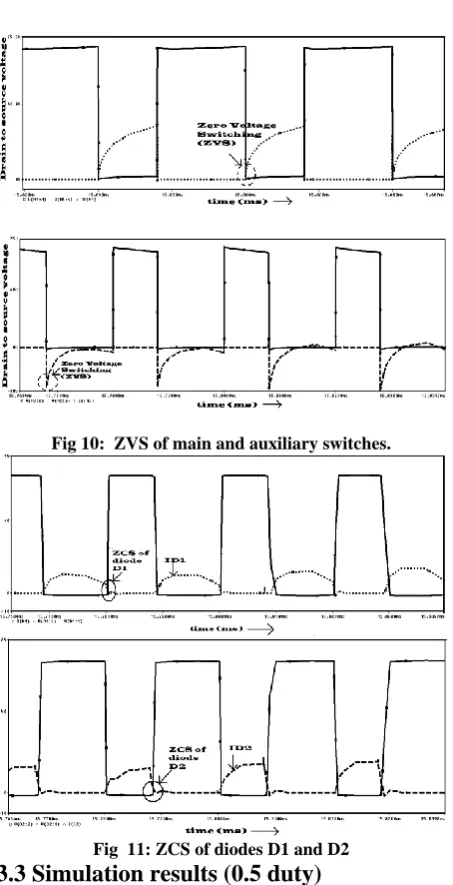
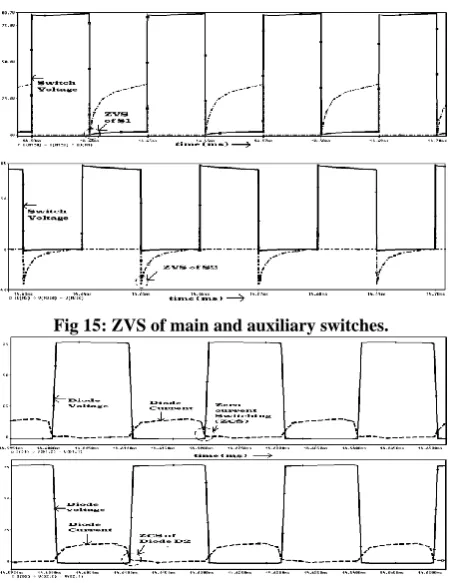
Fig. 9 shows the auxiliary inductor voltage and current waveforms; the negative voltage and current stresses are highly reduced compared to the soft switched boost converter. Fig. 10 shows the zero voltage turn-on of main and auxiliary switches. Fig. 11 shows the zero current turn-off of the diode D1 and D2. It is observed from Figs. 10 and 11 that the voltage
stress across device and diode is around 70V.
Fig 10: ZVS of main and auxiliary switches.
Fig 11: ZCS of diodes D1 and D2
3.3 Simulation results (0.5 duty)
Fig. 14 shows a four leg multiphase boost converter. This converter has P =2 and N = 2 to achieve 230V, 2.6 kW. The values of inductances and capacitances are same as that of the converter as mentioned in the section 3.1
A 230V, 2600W four leg multiphase boost converter with the designed inductance and capacitance values is simulated using PSpice 9.2. In this circuit the duty cycle is varied to improve the output power and it is equal to 0.5 and the voltage gain is almost 5 while the switching frequency is chosen as 50 kHz. Fig. 12 shows the gate pulse for main and auxiliary switches, a 10 volt pulse is applied for a total time period of 20µs. It is observed from Fig. 13 that the output voltage, current and power waveforms for the proposed multiphase boost converter meets the specifications. The load current is measured and found to be 11.4A. Fig. 14 shows the auxiliary inductor voltage and current waveforms. The voltage stress across the inductor is reduced (around 80V) compared to two stage boost converter. This is because of the low di/dt across the inductor due to the diode characteristics and sharing of output current in all the legs. Compared to a two leg converter, better sharing of output current takes place. This also contributes to low voltage stress across the inductor.
Fig 12: Gate pulse for main and auxiliary switches.
Fig 13: Output voltage, current and power waveforms.
Fig 14: Auxiliary inductor voltage and current waveforms.
Fig 15: ZVS of main and auxiliary switches.
Fig 16: ZCS of diodes D1 and D2.
4.
CONCLUSION
A multiphase boost converter suitable for high voltage gain and high power application has been proposed for a given voltage and power level. The existing converter has been modified by adding number of series cell and number of parallel cell to meet the voltage and power requirement. The modes of operation, analysis, design, and simulation results have been presented for a 230V, 2600W and 193V, 1860W load. For both the converters, it is observed that ZVS turn-on of the active switches and ZCS turn-off the diodes are achieved. In addition, it is found that the voltage stresses of the devices are much reduced compared to hard switched topologies.
5.
ACKNOWLEDGMENT
The authors wish to thank the management, faculty and friends of KPEC for extending their support and co-operation during this work.
6.
REFERENCES
[1] C. Wang, M. H. Nehir, and H. Gao, “Control of PEM fuel cell distributed generated systems”, IEEE Trans. Energy Convers.,vol.21, no.2, pp.586-595, Jun, 2006. [2] B. Duk Min, J. P.Lee, and E. H. Song, “ A novel
grid-connected PV PCS voltage transition PWM converters”, J. Power Electron, vol.8, no.4, pp. 309-316, Oct. 2008. [3] K. Liu, R. Oruganti, and F.C. Lee, “Resonant
switched-topologies and characteristics”, IEEE Trans. Power Electron, vol. PE-2, no.1, pp.62-74, Jan. 1987.
[4] V. Vorperian, “Quasi-square-wave converters: Topologies and analysis”, IEEE Trans. Power Electron., vol.3,no.2, pp. 183-191, Apr.1988.
[5] G. Hua, E.X. Yang, Y. Jiang, and F. C. Lee, “ Novel zero-current-transtion PWM converter”, IEEE trans. Power Electron., vol.9, no.6, pp.601-606, Nov.1994. [6] A. Ostadi, X. Gao, and G. Moschopoulos, “Circuit
properties of Zero-voltage –transition PWM converters”, J. Power Electron., vol.8, no.4, pp.35-50, Jan. 2008. [7] M. S. Elmore, “Input current ripple cancellation in
synchronized, parallel connected critically continuous boost converters”, in Proc, IEEE APEC, 1996, pp. 152-158.
[8] B. Eckardt, A. Hofmann, and S. Zeltner, “Automotive powertrain DC/DC converter with 2.5kW. dm3 by using SiC diodes”, presented at the ECPE CIPS conf., Nuremberg, Germany, Mar. 2008.
[9] T. Mizoguchi, T. Ohgai and T. Ninomiya, “A Family of singly-switch ZVS-CV DC-DC converters,” in Proc. IEEE APEC, 1994, vol.2,pp. 1392-1398.
[10]Jun Wen, Toatao Jin and Keyue Smedly, “A new interleaved isolated boost converter for high power applications”, IEEE proceedings,2009, pp.79-84. [11]Nam-Ju park, Dong-Seok Hyan, “N interleaved boost
converter with a novel ZVT cell using a single resonant inductor for high power applications”, IEEE proceedings, 2006, pp.2157-2161.
[12]Morton Nymand, Michael A.E. Andersen, “ A new primary-parallel boost converter for high-power and high-gain applications”, IEEE proceedings, 2009, pp.35-39.