AN EFFICIENT IMPLEMENTATION OF GRAPHICAL
CONVOLUTION TECHNIQUE USING SYNTHESIS
TOOL FOR COMMUNICATION RELEVANCE’S
Pathakota N V Koti Reddy
1, J.Koteshwar Rao
2, L.Srinivas Reddy
3 1M.Tech Scholar (VLSI),
2Asst. Professor (ECE),
3Assistant. Professor (ECE)
Nalanda Institute of Engg and Tech.
(NIET), Siddharth Nagar, Guntur, A.P. (India)
ABSTRACT
This article presents the efficient methodology to reduce the convolution processing time by using hardware
computation. Here we are implementing discrete linear convolution of two finite length sequences (NXN). Main
purpose of this analysis is we need to prove the possibility of FPGA that performs convolution on an image in
real time. In this paper, the proposed architecture is efficient and accurate in less time. Because of this
approach the computation speed increases and it has some more specializations like reduces power
consumption, less are and reduces hardware resources. This approach is coded in one of the hardware
description language, Verilog HDL and has tested on FPGA. It takes less area and hardware resources for
implementation.
Keywords
—
Serial In Parallel Out, Discrete Convolution, Multiplexer, Binary Multiplier
I.
INTRODUCTION
Convolution plays a key role in digital image processing. It performs on two discrete sequences and produces
another sequence. The major problem for convolution is it takes lot of time for processing. Our main approach is
to reduce the convolution processing time. Lot of approaches has made to solve this issue but those are limits for
some applications and this convolution is a mathematical process.
The following approaches, which has stated earlier than the proposed one.
1. In the article, “Handbook f Real-Time Fast Fourier Transforms”, the design approach is for fast convolve and
it performs its operation on CDMA signals. It operates on avoiding complex operations such as FFT based
convolves. In this design, the Walsh is used in place of FFT, which reduces the operations three times as
compared to FFT. It uses only real additions, because of this reason why it is faster than FFT. But, it increases
activity factor because of the increasing of hardware resources like RAM, counters and etc.
2. One of the image processing property, convolution filtering was using to achieve high performance by
utilizing parallelism and minimizing hardware cost. Different hardware structures are needed for different
applications because of the different filter widths. Because of this reason it is difficult to create a fixed parallel
efficient architecture.
3. As per “Low-Cost Fast VLSI Algorithm for Discrete Fourier Transform” the major problem for
implementation of convolution is area, speed and power factors, which effects on any DSP system. Coming to
other articles, “Parameterized convolution filtering in a field programmable gate array” and “The efficient
any hardware description language is increases the level of abstraction and allows other possible applications
while using for programmable devices.
4. The present days due to limitations of address space and limitations in ability to interface with other
surrounding systems, the DSP systems are suffering. To increase the bandwidth of a system, we need to use
high speed FPGAs with DSP systems, for this it provides additional functionalities to the system.
5. In an application linking spatial scaling of images, for example, a larger filter kernel could be able to be
required for large scale factors, modest scaling requires a small one. It must be expensive to implement the
entire largest desired filter kernel, and wasteful for small scale factors convolution. It can check all the phase
shifts in one step. The known FFT-based convolution has done this operation. Each FFT (or IFFT) requires
complex multiplications and additions as the amount of N logN and N logN respectively. Therefore, some
algorithms require approximately 3N (logN) + N complex multiplications and additions. The algorithm, which
is in parallel hardware implementation, will speed up the process. Other thing is the implementation itself is
very complex and requires a huge silicon area.
The behavior of a linear, time-invariant discrete-time system with input signal x[n] and output signal y[n] is
described by the convolution sum
The signal h[n], assumed known, is the response of the system to a unit-pulse input.
The convolution summation has a simple graphical interpretation. First, plot h[k] and the "flipped and shifted"
x[n - k]on the k axis, where n is fixed. Second, multiply the two signals to obtain a plot of the summand
sequence indexed by k, summing the values of this sequence with respect to k yields y[n]. These operations can
be repeated for every value of n of interest.
To explore graphical convolution, select signals x[n] and h[n] from the provided examples below, or use the
mouse to draw your own signal or to modify a selected signal. Then click at a desired value of n on the first k
axis. After a moment, h[k] and x[n - k] will appear. Drag the n symbol along the k axis to change the value of n.
For each n, the corresponding summand h[k] x[n - k] and output value y[n] will be displayed in their respective
windows.
II. LITERATURE SURVEY
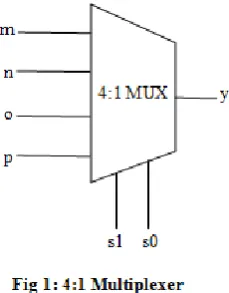
2.1 Multiplexer
Multiplexer, simply called as 2n:1 MUX is takes the inputs of multiple combinations of 2 like 2n and it gives
only one output. The output of multiplexer should be any one of the inputs only. That particular input can be
selected as per the selection line(s). In 2n, „n‟ indicates number of selection lines.
As per the above clarification,
2:1 MUX has 1 selection line,
4:1 MUX has 2 selection lines,
Block diagrams is drawn below.
The higher multiplexer can be implemented from the lower multiplexers. For example, 4:1 multiplexer can be
implanted from 2:1 multiplexers and 8:1 multiplexers can be implemented from 4:1 multiplexers or 2:1
multiplexers or both the combinations of 4:1 and 2:1 multiplexers. As same as the same procedure, all the higher
multiplexers has implemented from the lower multiplexers.
The selection of input is depending on „n‟ numbers. From those „n‟ number of selection lines, it takes the
possibilities of those numbers, for each possibility it takes one input as output.
Fig 2: 8:1 Multiplexer
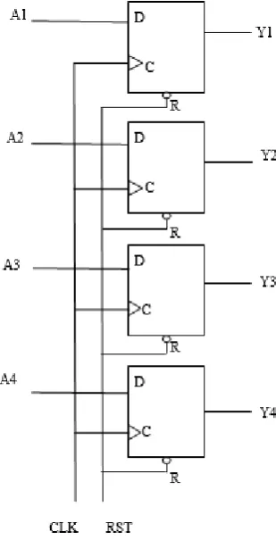
2.2 Register
There are many types of registers are available at the market. One of the register from those has shown in below
figure. Input data applies at input pin of the each flip flop. The clock present at each flip flop triggers, the input
Fig 4: 4-bit Register
To reset the register we have a clear input i.e., it clears all flip flops to 0. Register has another property to shift
the data from one flip flop to another flip flop. That could be right to left or left to right. A unidirectional 4-bit
shift register has displayed below.
Fig 5: 4-bit shift register
In the absence of Combinational logic, a circuit which is with flip flop is considered as a sequential circuit. One
bit storage element is known as flip flop. Combination of those flip flops has divided into two types of circuits
1) Registers
2) Counters
As we stated before, Register is group of flip flops, it holds some information, can available while running the
process. And it may have gates, which can able to perform some small data processing related tasks.
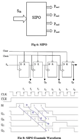
2.3 Serial in Parallel out (SIPO)
In this shift register, data has entered as serially like in Serial in serial out (SISO) and the outputs have to take as
SIPO, the data shifted serially through a single wire at input and after four clock pulses, the total data is in the
flip fops. Now, the output is present at every flip flop and w need to take as parallel. Block diagram of SIPO as
shown in below figure.
Fig 6: SIPO
Fig 8: SIPO Example Waveform
As shown in fig 7, Sin is the data input and the outputs are QA, QB, QC and QD are the outputs of givenregister.
We can able to know that there is another pin SO is there, generally it is not exist but it is useful any other
package may cascaded with it.
The clear signal is useful to clear all the flip flops when it is at active low i.e., logic „0‟. Clock signal is useful to
drive all the flip flops. Consider one example as 0110. When CLK is at „t1‟, the first bit „0‟ is forwarded to 1st
flip flop from Sin. At „t2‟, the first bit „0‟ is forwarded to second flip flop and 2nd bit from our data i.e., „1‟ is
enters into first flip flop. As the process moves on the total data is in all four flip flops after „t4‟ time. From it, as
the completion of four clock pulses the data is in all the four flip flops and we can collect it directly from QA, QB,
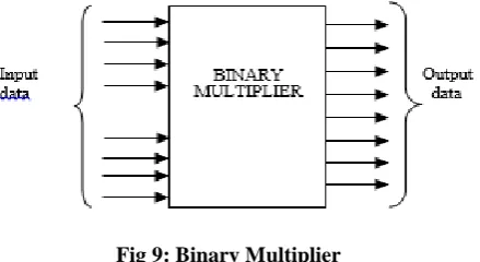
2.4 Binary Multiplier
The binary multiplier is used to multiply the two sequences. The block diagram of binary multiplier is shown in
fig 9.
Fig 9: Binary Multiplier
The binary multiplier is used to multiply the given data. Here we are representing the block diagrams of two
different sequences of 4 bits. It takes the both sequences and gives us the 8-bit output. Generally the output
contains 7 bits but MSB bit that is 8th bit is the carry bit of second MSB bit. So, the total bits of the output are 8
bits.
III. PROPOSED SYSTEM
The block diagram of proposed architecture has been shown in fig 10. Here we can observe that the two
sequences are applying as input of each containing 4 bits. One sequence is applied to one 4×1 multiplexer and
another sequence is applying for another 4×1 multiplexer. Selection of each bit is depending on the selection
lines of Multiplexers. After that the selected bit is sends to 4 bit SIPO register as serial. The process is same for
both the multiplexers and there is two different 4 bit SIPO registers have available for two multiplexers.
The outputs of two SIPO registers are taken as parallel of 4 bits from each SIPO. Those 8 bits have sends
directly to the binary multiplier as input data. The binary multiplier is important block of the convolution.
Multiplication process has accomplished in this block then the result is fed to the next block i.e., 8×1
multiplexer. As the process of multiplexer, it selects an input as its output depending upon the selection lines.
Here applied inputs are 8 so, number selection lines of the multiplexer is 3. After this process every input will
transfer into the register as shown in figure. We can collect our output at the register.
Note that the clock applied for every block synchronously. It will drive every block at same clock pulse.
IV. SIMLULATION RESULTS
The new method of convolution is designed and synthesised in Xilinx ISE13.2i .The synthesised results are
shown below wave forms
V. CONCLUSION
The convolution from various previous methods we derived new method of convolution. This design enhances
the speed and reduce the hardware complexity. This is designed using Verilog HDL and synthesised in Xilinx
ISE 13.2 i
REFERENCES
[1] John W. Pierre, (1996).“A Novel Method for Calculating the Convolution Sum of Two Finite Length
Sequences”,IEEE transaction on education, VOL. 39, NO. 1.
[3]. R. G. Shoup, (1994). “Parameterized convolution filtering in a field programmable gate array,” in selected
papers from the Oxford 1993 international workshop on field programmable logic and applications on More
FPGAs. Oxford, United Kingdom: Abingdon EE&CS Books, pp. 274–280.
[4]. Iván Rodríguez, (2008). “Parallel Cyclic Convolution Based on Recursive Formulations of Block
Pseudocirculant MatricesMarvi Teixeira”, IEEE, transaction on signal processing,
[5]. Thomas Oelsner, “Implementation of Data Convolution Algorithms in FPGAs”, QuickLogic Europe
http://www.quicklogic.com/images/appnote18.pdf
[6]. Chao Cheng , Keshab K. Parhi ,(2007). “Low-Cost Fast VLSI Algorithm for Discrete Fourier Transform”,
IEEE,. IEEE transaction on circuits and systems, VOL. 54.
[7]. J. I. Guo, C. M. Liu, and C. W. Jen, (1992).“The efficient memory-based VLSI array designs for DFT and
DCT,” IEEE Trans. Circuits Syst. II, Analog Digit. Signal Process., vol. 37, no. 10, pp. 723–733.
[8]. T. S. Chang, J. I. Guo, and C. W. Jen,(2000). “Hardware-efficient DFT designs with cyclic convolution and
AUTHOR DETAILS
PATHA KONDA N.V KOTI REDY, Pursuing M.tech (VLSI) from Nalanda institute
of Engineering and Technology (NIET), Siddharth Nagar, Kantepudi village, Satenepalli
Mandal, Guntur Dist, A.P, INDIA. His area of interest include DSP application in VLSI
such as high speed convolution of sequences.
J.KOTESHWAR RAO, he received his Master degree in VLSI. His area of interest
includes CMOS mixed signals and digital electronics. He currently working as
Asst.professor (ECE) from Nalanda institute of Engineering and Technology (NIET),
Siddharth Nagar, Kantepudi village, satenepalli Mandal, Guntur Dist , A.P,
L.SRINIVAS REDDY, He completed his post-graduation in DECS. His area of interest
includes digital electronics, digital communication, digital system design and VLSI
technology and design. His research areas are optimal communication technology. He is
currently working as Asst.professor (ECE) from Nalanda institute of Engineering and
Technology (NIET), Siddhartha Nagar, Kantepudi village, Satenepalli Mandal. Guntur