IJEDR1903016 International Journal of Engineering Development and Research (www.ijedr.org) 86
Performance Comparison of 1-bit Full Adders using
180 nm CMOS Technology
1Bhagyashree, 2Shashidhara K.S, 3Dr.Parameshwara M.C 1Student, 2Associate Professor, 3Associate Professor 1,2Nitte Meenakshi Institute of Technology, Bangalore, India
3Vemana Institute of Technology, Bangalore, India
_____________________________________________________________________________________________________
Abstract— This paper discusses the performance comparison of various state-of-the-art 1-bit full adder (FA) cells. All
these FA cells have been derived using static CMOS and its constituent logic styles such as pass transistor logic (PTL), transmission gate logic (TGL). The design of the state-of-the-art 1-bit FA cells is carried out using Cadences’ generic 180 nm based process design kit (GPDK). The performance of the FA cells is compared and analyzed in terms of design metrics (DMs) such as power, delay, power-delay-product (PDP), and area in terms of transistor count (TC). From the comparison results, for 1.8 V supply voltage and operating frequency 100 MHz, the average power consumption of Double-Pass Transistor Logic (DPL) based 1-bit FA is (143.1 µW) was found to be extremely low with moderately low delay (133.4 pS) and low PDP (19.08fJ). Further the FAs are analyzed in terms of DMs under variable load and power supply conditions.
Index Terms— full adder, adder, low power, PDP, 180 nm GPDK.
_____________________________________________________________________________________________________
I.INTRODUCTION
Addition is one of the fundamental arithmetic operations. It is used extensively in many ‘very large-scale integration’ (VLSI) systems such as application-specific ‘digital signal processing’ (DSP) architectures and microprocessors. In addition to its main task, which is adding two binary numbers, it is the nucleus of many other useful operations such as subtraction, multiplication, division, address calculation, etc. In most of these systems the adder is part of the critical path that determines the overall performance of the system. That is why enhancing the performance of the 1-bit FA cell (the building block of the binary adder) is a significant goal [1]. Different logic styles, each having its own merits and bottlenecks, was investigated to implement 1-bit full adder cells. The designs are broadly classified into: 1) static style and 2) dynamic style 3) pass transistor logic. Static full adders are generally more reliable, simpler with less power requirement but the on-chip area requirement is usually larger compared with its dynamic counterpart [2].In this paper eight different adders are studied in that DPL based FA cell provides high speed, low power, small area, low cost, low PDP under supply voltage of 1.8 V, operating frequency of 100MHz and load capacitance of 5.6 fF.
This paper discusses about the comparison and analysis of 8 1-bit FA cells in terms of their DMs. The rest of the paper is organized as follows: Section II discusses about the simulation setup used to extract the DMs of the FAs under consideration. Section III discusses about the simulation results and Section IV about the conclusion.
II.SIMULATION SET-UP
Generic simulation test bench used is shown in Fig-1. Along with the transistor sizes of each buffer. The performance of the ‘circuit under test’ (CUT) is evaluated in terms of worst-case delay, power consumption, and power-delay product for a range of supply voltages (0.8–1.8 V) at 100 MHz frequency. The delay is calculated from 50% of voltage level of input to 50% of voltage level of resulting output all the rise and fall output transitions. For the calculation of the power-delay product, worst-case delay is chosen to be the larger delay amongst the two outputs. Different loading conditions are also considered to evaluate the performance of the test circuits (5.6–100 fF) [5]. The test input pattern used to calculate the power dissipation, worst case delay, and PDP of a CUT is shown in Fig-2.
IJEDR1903016 International Journal of Engineering Development and Research (www.ijedr.org) 87
Fig.2: Standardinput stimulus used
to extract power, delay, and PDP of a CUT III.SIMULATION RESULTS
All eight 1- bit FA cells: 14T , HPSC and NEW-HPSC, Hybrid-CMOS FA, TFA, CMOS FA, SR-CPL FA [1-6], are simulated with Cadences’ Spectre using generic 180nm MOSFET models to determine their worst-case delay, average power, and PDP.Study is performed in 2 steps. In the first step, the study of the performance metrics are compared for the adder circuits as a function of supply voltage Vdd variation from 0.8V to 1.8V, at 5.6fF load capacitance CL, and a maximum input speed of
100MHz.In the second step the performance metrics are again studied as a function of the load capacitance CL, varied from
5.6fF to 100fF, at VDD=1.8V, and maximum input speed at 100MHz. Then keeping the load capcitance constant i.e 5.6fF and Vdd=1.8 in these three conditions the performance DMs can be analysed.
The 14T , HPSC and NEW-HPSC, Hybrid-CMOS FA, TFA, CMOS FA, SR-CPL FA, are the CUTs, simulated under identical ‘process-voltage-temperature’ (PVT) conditions to compare their power, delay, and PDP performance metrics. The performance metrics for the 8 circuits are compared through parameterization of the Vdd and CL [5].
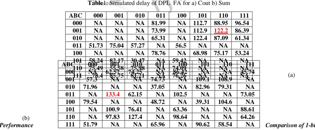
Simulated Delay Metrics For Cout And Sum
For a 1-bit adder with 3 inputs A, B, and C, there are 23=8 possible input vectors. For an exhaustive delay analysis for Sum
or carry (Cout), we need to consider all possible input vector transitions. There are 2k×2k-1=56 numbers of input vector
transitions for k=3. All the 56 input vector transitions are defined as standard input test patterns, to determine the worst-case delay in Sum or Carry. All eight adders: 14T, HPSC, NEW-HPSC, Hybrid-CMOS FA, TFA, CMOS FA, and SR-CPL FA, respectively. Each delay matrix consists a total of 64 cells; the 8 cells of which along diagonal corresponds to the transitions within the same input vector states, i.e., 000 → 000, →001 → 001, → 111 → 111, are insignificant. Further, for 24 input vector transitions, there will be no corresponding transitions in the outputs, labelled ‘Not Applicable’ (NA) in Table (1). Each of the remaining 64-8=56 non-diagonal cells are partitioned into two sub-cells viz., sub-cell Sum (first, in a cell), and sub-cell Cout (second, in a cell). Further, 56-24=32-delays in Sum and, corresponding 32 delays in Carry have been simulated [5-6].
Table 1 shows the vector transition of delay for Sum and Cout of a DPL FA, the table have 64 transition in that 32 transitions are not applicable, the aim of this vector table is to achieve the maximum worst case delay. The table shows the example vector transition of DPL FA. From this table the maximum worst case delay is found to be 133.4 pS, this occur for the transition from 001-011 at Sum output. The worst-case delay of a CUT is the maximum delay among the outputs Sum and Cout. The worst case of a DPL FA is Tdworst= max (Tdworst, sum ,Tdworst, cout) =max(133.4 pS, 122.2 pS) =133.4 pS
Table1: Simulated delay of DPL FA for a) Cout b) Sum
(a)
(b)
Performance Comparison of 1-bit FA cells
The performance comparison of 1-bit FA cells in terms of DMs is shown in the Table-2. All the DMs are extracted under common PVT conditions using the test bench shown in Fig-1. From this table it is found that the DPL FA cell is found to be more efficient than any other FA cell under consideration.
ABC 000 001 010 011 100 101 110 111 000 NA NA NA 81.99 NA 112.7 88.95 96.54 001 NA NA NA 73.99 NA 112.9 122.2 86.39 010 NA NA NA 65.31 NA 122.4 87.09 61.34 011 51.73 75.04 57.27 NA 56.5 NA NA NA 100 NA NA NA 78.76 NA 68.98 75.17 53.24 101 58.24 82.17 30.47 NA 59.42 NA NA NA 110 75.49 55.58 75.98 NA 74.09 NA NA NA 111 78.4 85.75 81.21 NA 76.26 NA NA NA
ABC 000 001 010 011 100 101 110 111
000 NA 62.57 74.25 NA 86.42 NA NA 45.74 001 57.3 NA NA 74.73 NA 109.1 108.9 NA 010 71.96 NA NA 37.05 NA 82.96 79.31 NA
011 NA 133.4 62.15 NA 102.5 NA NA 73.05
IJEDR1903016 International Journal of Engineering Development and Research (www.ijedr.org) 88 Table 2: Performance comparison of 1-bit FA cells
FA Adder FA Cell Delay (pS) Power (µW) PDP (fJ)
NEW 14T FA FA1 239.3 279.5 66.76
HPSC FA FA2 318 337.7 107.38
NEW-HPSC FA FA3 246.6 312.6 76.89
Hybrid-CMOS FA FA4 294.2 298.2 87.73
TFA FA5 161.5 237.8 38.40
CMOS FA FA6 228.8 318.7 72.91
SR-CPL FA FA7 173.6 147.5 25.606
DPL FA FA8 133.4 143.1 19.08
DMs as a function of load capacitance and temperature
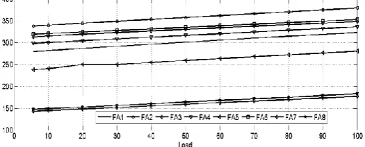
Fig-3 is the plot of worst-case delay as a function of load capacitance. This graph is plotted for 8 1-bit FA cells namely FA1 to FA8. The minimum load capacitance to extract the worst-case delay considered is 5.6 fF and maximum load capacitance is 100 fF. From this graph it is clear that as the load capacitance increases the worst delay is also increasing in a linear scale. In this graph all the worst-case values under various capacitance loads are extracted under common PVT conditions. The simulation results are extracted under the common PVT conditions: the supply voltage is 1.8 V, and Temperature is 270C. The
input signal frequency used to extract the delay is 100 Mhz.
Fig.3: Plot of delay as a function of Load Capacitance
Fig-4 shows the graph of worst-case delay as a function of temperature. The lowest temperature to extract the normalized delay is considered as 270C and the supreme temperature is 1100C. As the temperature increases the delay will also
increase up.
Fig.4: Plot of delay as a function of Temperature
Fig-5 illustrate the power as function of normalized load capacitance. The minimum load capacitance considered to extract the power is 5.6 fF and extreme load capacitance is 100 fF. From this graph it is found that, as the load capacitance increases, the power dissipation also increases in a linear way.
IJEDR1903016 International Journal of Engineering Development and Research (www.ijedr.org) 89 Fig-6 shows the graph of worst-case delay as a function of temperature. The lowest temperature to extract the normalized delay is considered as 270C and the supreme temperature is 1100C. As the temperature increases the power will
also increase up.
Fig.6: Plot of Power as a function of
Temperature
Fig-7 illustrates the PDP as function of
normalized load capacitance. The minimum load capacitance considered to extract the power is 5.6 fF and extreme load capacitance is 100 fF. From this graph it is found that, as the load capacitance increases, the PDP also increases in a linear way.
Fig.7: Plots of PDP as a function of Load Capacitance
Fig-8 shows the graph of PDP as a function of temperature. The lowest temperature to extract the normalized delay is considered as 270C and the supreme temperature is 1100C. As the temperature increases the PDP will also increase up.
Fig.8: Plot of PDP as a function of Temperature
IV.CONCLUSION
An extensive performance analysis and comparison of 1-bit full-adder cells have been presented. The 8 FA cells are implemented, simulated, analyzed, and compared under common PVT conditions using Cadence’s generic 180 nm MOSFET models. Finally, it is found that the DPL FA cell dissipates low power and has low delay. Thus, it is useful for energy efficient applications.
REFERENCES
[1] Ahmed M. Shams, Tarek K. Darwish,Magdy A. Bayoumi, “Performance Analysis of Low-Power 1-Bit CMOS Full Adder Cells: IEEE TRANSACTIONS ON VERY LARGE-SCALE INTEGRATION (VLSI) SYSTEMS, VOL. 10, and NO. 1, FEBRUARY 2002.
[2] Partha Bhattacharyya, Bijoy Kundu, Sovan Ghosh, Vinay Kumar, Anup Dandapat, “Performance Analysis of a Low-Power High-Speed Hybrid 1-bit Full Adder Circuit”, IEEE TRANSACTIONS ON VERY LARGE-SCALE INTEGRATION (VLSI) SYSTEMS, VOL. 23, NO. 10, OCTOBER 2015.
[3] Sumeer Goel, Ashok Kumar, Magdy A. Bayoumi,“Design of Robust, Energy-Efficient Full Adders for Deep-Submicrometer Design Using Hybrid-CMOS Logic Style”, Document, IEEE TRANSACTIONS ON VERY LARGE-SCALE INTEGRATION (VLSI) SYSTEMS, VOL. 14, NO. 12, DECEMBER 2006.
[4] R.P. MeenaakshiSundari, Dr. R Anita, M.K. Anandkumar,“Implementation of Low Power CMOS Full Adders Using Pass Transistor Logic”IOSR Journal of VLSI and Signal Processing (IOSR-JVSP) Volume 2, Issue 5 (May. – Jun. 2013), PP 38-43 e-ISSN: 2319 – 4200, p-ISSN No.: 2319 – 4197.
IJEDR1903016 International Journal of Engineering Development and Research (www.ijedr.org) 90 [6] M. C. Parameshwara, H. C. Srinivasaiah, “Low-Power Hybrid 1-Bit Full-Adder Circuit for Energy Efficient Arithmetic