Volume-7 Issue-1
International Journal of Intellectual Advancements
and Research in Engineering Computations
Design and implementation of arithmetic and logical block using QCA
technology
T. Ashok, M Chandrasekar
Head of the Department, Department of ECE, MAM School of Engineering, Trichy.
Associate Professor, Department of Electronics and Communication, MAM School of Engineering
ABSTRACT
In this paper an eight bit arithmetic and logical block is designed using QCA technology. QCA cells does not conducts the information as current as used in conventional logic circuits. It operates based on the concept of Columbic Interaction of the states of electrons in QCA cells. So, designing of eight bit ALU block at low power can be achieved by using QCA technology.
Index Terms:
QCA Technology, Columbic Interaction, Conventional Logic Circuits.INTRODUCTION
The QCA cell In contrast to electronics based on transistors, QCA does not operate by the transport of electrons, but by the adjustment of electrons in a small limited area of only a few square nanometers. QCA is implemented by quadratic cells, the so-called QCA cells. In these squares, exactly four potential wells are located, one in each corner of the QCA cell (see figure 1). In the QCA cells, exactly two electrons are locked in. They can only reside in the potential wells. The potential wells are connected with electron tunnel junctions. [1-5]
There are two diagonals in a square, which means the electrons can reside in exactly two possible adjustments in the QCA cell. Regarding these two arrangements, they are interpreted as a binary '0' and binary '1', i.e. each cell can be in two states. The state '0' and the state '1', as shown in figure 3. A binary system is something familiar, as boolean logic is used already in today's computers. There, a high voltage is often interpreted as binary '1' and a low voltage as binary '0'. [6-10]
Information and data propagation
If two QCA cells are placed next to each other, it is possible to exchange their states, i.e. the
adjustments of the electrons in them. The QCA cell that should transfer its state to a neighboring cell must have its tunnel junctions closed, the tunnel junctions in the neighboring cell have to be open, to allow the electrons to travel through the tunnel junctions between the potential wells. As soon as they open, the electrons in the neighboring cell are pushed by the Coulomb force of the original cell as far away as possible. [11, 12]
As they also are pushed away from each other, they will travel into the same potential wells as in the original cell. As soon as the tunnel junctions are closed again, the transfer of the state is completed. The state of a cell can also be transferred to multiple neighboring cells. It works the very same way as with a single neighbor cell, but the tunnel junctions of all the sequentially neighboring cells should be open at the same time, which makes the transfer much faster than transferring the state cell by cell. This allows us to build “wires”, made of QCA cells, to transport information over larger distances.
They can be opened for the electrons to travel through them under a particular condition, by a clock signal. A later chapter will cover this in more detail. Without any interaction from outside, the two electrons will try to separate from each other as
Copyrights © International Journal of Intellectual Advancements and Research in Engineering Computations, far as possible, due to the Coulomb force that
interacts between them. As a result, they will reside in diagonally located potential wells, because the diagonal is the largest possible distance for them to reside.
The existing literature on QCA design mostly uses a gate-based methodology. Wales et al (2003) and Zhang et al (2004) have worked on this methodology. In a gate-based design, much like a CMOS design process, first the desired logic function of the circuit is determined and then a logic synthesis process is performed to obtain a net list.
A logic gate is an electronic circuit that performs a logic function on number of input
binary signals. The logic gate is the building block from which many different kinds of logic circuit can be constructed. The basic logic gates are OR, AND, NOT, NAND and NOR. The NAND and NOR gates are called as the universal gates. The exclusive OR (XOR) is another logic gate which can be constructed using the basic gates.
BASIC ELEMENTS AND GATES
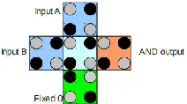
So far, we know how to interpret and transport information with QCA cells, but yet we lack the possibility for computations. For QCA cells the basic gate is a three-input majority vote. It is built from five cells, arranged as a cross.
QCA Majority voter
Majority voter
From physics, it is know that the Coulomb forces of several electrons sum up. The majority voter takes advantage of this effect. The cells on top, at the left and at the bottom work as input connection cells. As the Coulomb forces of the electrons of all input cells sum up, the middle cell adjusts to the majority of adjustments of the input connection cells. Finally the output cell adjusts to the middle cell and the resulting state of the majority vote can be obtained from the output cell. QCA AND gate As we work in the field of QCA with the known binary representation, it is preferable to have further logic gates we are
already familiar with. By a slight modification, it is possible to turn the majority voter into an AND gate.
The Boolean AND outputs 1 if all inputs are 1, otherwise 0. Regarding two inputs of the majority vote, as the inputs of an AND gate, and the voter should not output 1 if only one of the two inputs is one, a fixed cell is added as third input, that always is in the 0 state. If both AND inputs are 1, the two 1s sum up to a stronger Coulomb force than the single fixed 0 cell and the majority voter is turned into a two-input AND gate. The fixed cell can be obtained by setting it to the 0 state and never open the tunnel junctions.
Fig. QCA AND gate
QCA OR gate
The OR gate is built almost exactly like the AND gate, but instead of a fixed 0, a fixed 1 QCA cell must be attached as one input. The fixed 1 cell
Fig.4.3. QCA OR gate
QCA NOT gate
It is also possible to build a QCA NOT gate. The implementation in QCA takes advantage of geometry of cell adjustments. One QCA wire is forked to two wires, the switch of the cell adjustment takes place by putting the output cell next to the forked wires so that only corners are touching.
Since only cell corners are touching right of the fork and the cells at the end of the fork will have the same adjustment and the cell on the right of the fork will not adjust with an electron close to an electron at the corner at the end of the fork, the adjustment right of the fork will be inverted. This makes a 1 at the input a 0 at the output and vice versa.
Fig. QCA NOT gate
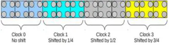
Clock zones
Clock zones are a tricky challenge of QCA. They avoid random adjustments of QCA cells and “guide” the information flow, in particular the data propagation, through QCA circuits. In contrast to
transistor-based circuits, one clock cycle consists of four clock signals, which are delayed by ¼ of the whole clock cycle among each other, as depicted in figure.
Fig. The Four Shifted Clock Signal
The figures in this chapter will always show clock zones like clock 0, clock 1 and so on. This is for convenience; of course you can also read it as clock n, clock n+1, clock n+2. Important is, that particular groups of QCA cells are in different clock zones. When the clock signal is high, it opens
Copyrights © International Journal of Intellectual Advancements and Research in Engineering Computations, There is a rough upper limit for the size of one
clock zone. In QCA wires with almost no other QCA cells near the wire, i.e. with no Coulomb force “noise” from the surrounding, clock zones can be large. In areas with QCA cells around the wire, the clock zones must be smaller. There is no strict rule for the size of a clock zone dependent on the surrounding noise, but in general it turns out that in noisy areas clock zones might have to be as small as only two QCA cells.
In areas with almost no noise, clock zones can be built as large as 12-14 QCA cells. Though there are no strict rules where to begin and end a clock zone, there is some best practice, how to put clock zones around the basic gates, presented in the previous chapters. When you design QCA circuits, we strongly recommend to stick to these clock zones, there exist only very rare cases where clock zones around the basic gates can differ without affecting reliable data propagation.
QCA circuit design
QCA is a technology, not yet being ready for the market. As a result, you will design and simulate QCA circuits. For this, you will use the QCA Designer software which allows design of circuits with an easy to use graphical user interface. The simulation is also done with QCA Designer. We chose QCA Designer, as it is the most realistic simulator from a physical point of view, so your simulations will be very exact. The very realistic simulation allows you to detect disturbances of neighboring QCA cells or cell areas that should not interact with each other. As a first example for a complete QCA circuit, we begin with a 1 bit adder as shown in figure 16. Different colors mean different clock zones, beginning with green, cyan, light blue and white.
The blue QCA cells, labeled A and B, are input cells of the adder. As you can see, both type of cells, symmetric and regular ones, are used in this circuit, because it requires wire crossings. The four orange cells are “fixed” cells to build AND and OR gates from majority voters. The yellow cells are output cells, labeled S for sum and C for the carry bit. If you follow the clock zones in each path of the circuit, you will see that the adder needs 2 ¼ clock cycles to display the result at the output cells,
i.e. the data in each path travels through 9 sequential clock signals.
It is also possible to verify that the QCA adder is correct. A simple 1 bit adder can be described by these two formulas: S= A B A B and C=AB. This means that the output S should become 1 when either A is 0 but B is 1 or when A is 1 but B is 0. C should become 1 when A and B are 1.
These formulas are implemented in QCA 1 bit adder. If one follows the inputs to the top half of the circuit, there once A, once B, are negated and connected to the not negated other input in an AND gate. Near the output S is the OR gate. C can be verified easily, the inputs are connected in the AND gate at the bottom of the circuit.
The logic gates have two or more inputs and only one output except for the NOT gate, which has only one input. The output signal appears only for certain combinations of the input signals. The manipulation of binary information is done by the gates. Each gate has a distinct logic symbol and its operation can be described by means of an algebraic function. The relationship between input and output variables of each gate can be represented in a tabular form called a truth table.
In this thesis different types of logical structures are designed using three different QCA gates such as Majority gate, Nand-Nor-Inverter and And- Or-Inverter. Then the designed structures are implemented by QCA cells using cell minimization techniques. The designed structures are simulated by QCA Designer. The simulation based performance analysis of these structures are tabulated and compared with existing majority gate method.
CELL MINIMIZATION TECHNIQUES
The area and complexity are important key issues in circuit designs. In QCA technology, the area and complexity can be minimized by reducing the number of cells. Hence the following cell minimization techniques are proposed in this thesis.
Two cell inverter
two cell inverter is used for circuit implementations.
QCA computation proceeds by orientation of cells based on polarization of neighboring cells. QCA inverter can be implemented by positioning and rotation of cells. In our implementation, positioning of QCA cell is used to invert the output from input logic level. In the two cell inverter,
First cell is placed normally and the second cell is placed adjacent to the first cell, but 10nm vertically below from the cell as shown in Figure 4.1. Here the electrostatic interaction is inverted because the quantum dots of different polarizations are misaligned between the cells.
Fig .QCA two cell inverter
Proper Alignment of cells
This is the second technique used to minimize the number of cells in the QCA circuits. The following rules are used to minimize the number of cells.
Rules
1. The minimum distance between the adjacent rows of cells is the width of two cells.
2. The minimum distance between the adjacent columns of cells is the width of two cells.
3. The number of cells in the rows need not be equal.
4. The number of cells in the columns need not be equal.
5. At least one extra cell is used to carry
input or catch the output.
6. The designed circuits are implemented with suitable arrangement of cells without overlapping of neighboring cells.
DESIGN OF LOGICAL STRUCTURES
USING MAJORITY GATE
Various types of QCA devices can be constructed using different physical cell arrangements. One of the basic logic gates in QCA is the majority voter (MV) and the inverter (INV) is the other basic gate in QCA. The other logical structures are designed using these two gates. Logic operations are performed by means of the interactions between adjacent cells.
CIRCUIT IMPLEMENTATION
MODULE EXPLANATION
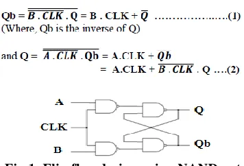
Fig.1. Flip flop design using NAND gate Using the derived expression in equation 1 and
equation 2, and also with the flip flop using NAND gate, we can simply construct any flip-flop in a much easier way just by modifying the inputs. All
Copyrights © International Journal of Intellectual Advancements and Research in Engineering Computations,
Truth table
The flip-flops are designed
SR Flip-flop D flip-flop JK flip-flop T flip-flop.
BLOCK DIAGRAM
SR FLIP-FLOP
The S-R flip-flop has two inputs namely, SET(S) and RESET(R), and two outputs Q and Qbar which are complement to each other. The clock pulse input acts as an enable input to the other two inputs S and R. We have simply replaced A by S and B by R from our proposed equation to generate SR flip-flop.
D FLIP-FLOP
The D flop is called Delay (D) flip-flop as it introduces a delay between input and output. We have easily constructed D flip-flop from
our proposed logic just by replacing A by D and B
by.
JK FLIP-FLOP
The limitation of SR flip-flop is overcome in JK flip-flop. The inputs J and K behave as inputs S and R to set and reset the flip-flop respectively.
T FLIP-FLOP
Another basic flip-flop, called T or trigger or toggle flip-flop has only a single data (T) input, a clock input and two outputs Q and Qb. The T-type flip-flop is designed from a J-K flip-flop by
connecting its J-K inputs together. The term T comes from the ability to ‘toggle’ or complement its state and are also called single input JK flip-flop. Here we have assumed inputs J and K both as T and they are tied together
DESIGINING ALU BLOCK
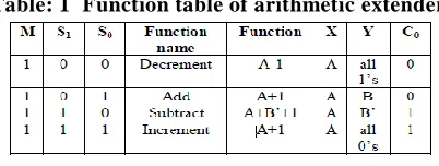
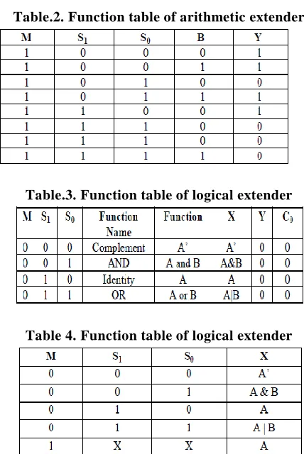
The Arithmetic Logic Unit (ALU) performs the basic arithmetic and logical operation and consists of arithmetic extender, logical extender and one bit full adder as shown in figure 5.Three control signals determine the operation of the ALU. M is
the mode control variable used to select between arithmetic and logical operations. S1 and S0 are used in combination with M to select between the eight arithmetic and logical operation the ALU supports.
Fig. Architecture of ALU
Extender
The Arithmetic extender modifies the second operand and passes it to the Full adder to the arithmetic.
According to truth table we write Boolean equation of arithmetic extender shown in equation (1) and design logic circuit of
arithmetic extender shown in fig. 6.
𝑌 = 𝑀𝑆1’ 𝐵 + 𝑀𝑆0’ 𝐵 … (1)
Logical Extender
The logic operations are performed in the logic extender. The FAs are used simply as connection for the outputs.
Copyrights © International Journal of Intellectual Advancements and Research in Engineering Computations, Table.2. Function table of arithmetic extender
Table.3. Function table of logical extender
Table 4. Function table of logical extender
According to truth table we write Boolean equation of logical extender shown in equation (2)
and design logic circuit of logical extender shown in fig..
Fig. Logic circuit of Arithmetic Extender, Logic circuit of Logical Extender
Full Adder
Full adder performs the addition of three bits. In full adder, we have given three inputs X, Y and C0, where C0 is carry in signals shown in equation (3).
Truth table of full adder
The Boolean equations for Full adder are shown in equations (4) & (5) and logic circuit of full adder as shown in figure 8.
𝐹 = 𝑋⊕𝑌⨁𝐶0 … (4)
𝐶𝑜𝑢𝑡 = 𝑀𝑉𝑋, 𝑌, 𝐶0 … (5)
Copyrights © International Journal of Intellectual Advancements and Research in Engineering Computations, This fully programmable eight bit arithmetic
and logical block has been designed using QCA technology at 1.8 V power supply. Its speed is 45% duty cycle greater than existing technology. It consumes 600 μW.
CONCLUSION
The designing of arithmetic and logical block in eight bit by using QCA technology has been designed .QCA Designer tool and gtk2 runtime environment tool has been used in this design. Total power consumption is 600 μW. So, Power dissipation is minimized. This paper is useful in low power VLSI design.
REFERENCES
[1]. Lent, Craig S., and P. Douglas Tougaw. "Lines of interacting quantum‐ dot cells: A binary wire", Journal of applied Physics 10(74), 1993, 6227-6233.
[2]. P. D. Tougaw, C. S. Lent, “Logical devices implemented using quantum cellular automata”. Journal of Applied Physics 75(3), 1994, 1818–1825.
[3]. C. S. Lent, and P. D. Tougaw, “A device architecture for computing with quantum dots”, Proceedings of the IEEE, 85(4), 1997, 541- 557.
[4]. A.O. Orlov, I. Amlani, G.H. Bernstein, C.S. Lent, G.L. Snider, “Realization of a Functional Cell for Quantum-Dot Cellular Automata”, Science, 277, 1997, 928-930.
[5]. A. O. Orlov, I. Amlani, C. S. Lent, G. H. Bernstein, and G. L. Snider, “Experimental demonstration of a binary wire for quantum-dot cellular automata”, Appl. Phys. Lett., 74, 1999, 2875–2877.
[6]. R.Companio, L. Molenkamp and D.J. Paul, Technology Roadmap for Nanoelectronics, 2000.
[7]. J. Timler, and C.S. Lent, “Power gain and dissipation in Quantum-dot Cellular Automata”, Journal of Applied Physics, 91(2), 2002, 823- 831.
[8]. Craig S. Lent andBeth Isaksen, “Clocked molecular quantum-dot cellular automata”, IEEE Transaction on Electron Devices 50(9), 1890-1896.
[9]. K Walus, T. J. Dysart, G.A. Jullien and R.A. Budiman, “QCA Designer: a rapid design and Simulation tool for quantum-dot cellular automata”, IEEE Transaction on Nanotechnology, 3, 2004, 26-31.
[10]. M. Ottavi, V. Vankamamidi, F. Lombardi, Clocking and cell placement for QCA, in: Proceedings of the IEEE Nanotechnology Conference, 2006, 343– 346.
[11]. S. Srivastava; S. Sarkar; S. Bhanja, “Power Dissipation Bounds and Models for Quantum-dot Cellular Automata Circuits”, 2006. IEEE-NANO, Sixth IEEE Conference on Nanotechnology, 2006.