A Vision Chip for Color Segmentation and Pattern
Matching
Ralph Etienne-Cummings
Iguana Robotics, P.O. Box 625, Urbana, IL 61803, USA
Department of Electrical and Computer Engineering, Johns Hopkins University, Baltimore, MD 21218, USA Email:[email protected]
Philippe Pouliquen
Iguana Robotics, P.O. Box 62625, Urbana, IL 61803, USA
Department of Electrical and Computer Engineering, Johns Hopkins University, Baltimore, MD 21218, USA Email:[email protected]
M. Anthony Lewis
Iguana Robotics, P.O. Box 625, Urbana, IL 61803, USA Email:[email protected]
Received 15 July 2002 and in revised form 20 January 2003
A 128(H)×64(V)×RGB CMOS imager is integrated with region-of-interest selection, RGB-to-HSI transformation, HSI-based pixel segmentation, (36bins×12bits)-HSI histogramming, and sum-of-absolute-difference (SAD) template matching. Thirty-two learned color templates are stored and compared to each image. The chip captures the R, G, and B images using in-pixel storage before passing the pixel content to a multiplying digital-to-analog converter (DAC) for white balancing. The DAC can also be used to pipe in images for a PC. The color processing uses a biologically inspired color opponent representation and an analog lookup table to determine the Hue (H) of each pixel. Saturation (S) is computed using a loser-take-all circuit. Intensity (I) is given by the sum of the color components. A histogram of the segments of the image, constructed by counting the number of pixels falling into 36 Hue intervals of 10 degrees, is stored on a chip and compared against the histograms of new segments using SAD comparisons. We demonstrate color-based image segmentation and object recognition with this chip. Running at 30 fps, it uses 1 mW. To our knowledge, this is the first chip that integrates imaging, color segmentation, and color-based object recognition at the focal plane.
Keywords and phrases:focal plane image processing, object recognition, color histogramming, CMOS image sensor, vision chip, VLSI color image processor.
1. INTRODUCTION
CMOS-integrated circuits technology readily allows the in-corporation of photodetector arrays and image processing
circuits on the same silicon die [1, 2,3,4,5,6]. This has
led to the recent proliferation in cheap and compact
dig-ital cameras [7], system-on-a-chip video processors [8,9],
and many other cutting edge commercial and research imag-ing products. The concept of usimag-ing CMOS technology for combining sensing and processing was not spearheaded by the imaging community. It actually emerged in mid ’80s from the neuromorphic engineering community developed
by Mead and collaborators [10,11]. Mead’s motivation was
to mimic the information processing capabilities of
biolog-ical organisms; biology tends to optimize information ex-traction by introducing processing at the sensing
epithe-lium [12]. This approach to sensory information processing,
which was later captured with terms such as “sensory pro-cessing” and “computational sensors,” produced a myriad vi-sion chips, whose functionality includes edge detection, mo-tion detecmo-tion, stereopsis, and many others (examples can be
found in [13,14,15,16]).
in CMOS technologies using no additional lithography lay-ers. On the other hand, color image processing has been lim-ited primarily to the commercial camera arena because three additional masks are required to implement R, G, and B
fil-ters [17]. The additional masks make fabrication of
color-sensitive photodetection arrays expensive and, therefore, not readily available to researchers. Nonetheless, a large part of human visual perception is based on color information pro-cessing. Consequently, neuromorphic vision systems should not ignore this obviously important cue for scene analysis and understanding. This paper addresses this gap in the sili-con vision literature by providing perhaps the only integrated large array of color photodetectors and processing chip. Our chip is designed for the recognition of objects based on their color signature.
There has been a limited amount of previous work on neuromorphic color processing. The vast majority of color processing literature addresses standard digital image pro-cessing techniques. That is, they consist of a camera that is connected to a frame grabber that contains an analog-to-digital converter (ADC). The ADC interfaces with a analog-to-digital computer, where software algorithms are executed. Of the few biologically inspired hardware papers, there are clearly two approaches. The first approach uses separate imaging
chips and processing chips [18], while the second approach
integrates a handful of photodetectors and analog
process-ing circuitry [19]. In the former example, standard
cam-eras are connected directly to analog VLSI chips that demul-tiplex the video stream and store the pixel values as
volt-ages on arrays of capacitors. Arrays as large as 50×50
pix-els have been realized to implement various algorithms for
color constancy [18]. As can be expected, the system is large
and clumsy, but real-time performance is possible. The sec-ond set of chips investigate a particular biologically inspired problem, such as RGB-to-HSI (Hue, saturation, and inten-sity) conversion using biologically plausible color opponents and HSI-based image segmentation using a very small num-ber of photodetectors and integrated analog VLSI circuits
[19]. Clearly, the goal of the latter is to demonstrate a
con-cept and not to develop a practical system for useful im-age sizes. Our approach follows the latter, however, we also use an architecture and circuitry that allow high-resolution imaging and processing on the same chip. In addition, we include higher-level processing capabilities for image recog-nition. Hence, our chip can be considered to be a func-tional model of the early vision, such as the retina and vi-sual area #1 (V1) of the cortex, and higher vivi-sual cortical regions, such as the inferotemporal area (IT) of the cortex [20,21].
2. COLOR SEGMENTATION AND PATTERN MATCHING
In general, color-based image segmentation, object identifi-cation, and tracking have many applications in machine vi-sion. Many targets can be easily segmented from their back-grounds using color, and subsequently can be tracked from frame to frame in a video stream. Furthermore, the
tar-gets can be recognized and tagged using their color
signa-ture. Clearly, in the latter case, the environment must be configured such that it cooperates with the segmentation process. That is, the targets can be colored in order to fa-cilitate the recognition process because the recognition of natural objects based solely on color is prone to false posi-tives. Nonetheless, there are many situations where color seg-mentation can be directly used on natural scenes. For ex-ample, people tracking can be done by detecting the pres-ence of skin in the scene. It is remarkable that skin, from the darkest to the lightest individual, can be easily tracked in HSI space, by constructing a model 2D histogram of the Hue (H) and saturation (S) (intensity (I) can be ig-nored) of skin tone in an image. Skin can be detected in other parts of the image by matching the histograms of
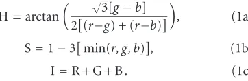
these parts against the HS model. Figures1and2show an
example of a general skin tone identification task, imple-mented in Matlab. Conversely, specific skin tones can be de-tected in a scene if the histogram is constructed with specific examples. The latter will be demonstrated later using our chip.
Color imagers, however, provide an RGB color represen-tation. For the above example, a conversion from RGB to HSI is required. There are other benefits of this conversion. The main advantage of the HSI representation stems from the ob-servation that RGB vectors can be completely redirected un-der additive or multiplicative transformations. Hence, color recognition using RGB can fail under simple conditions such as turning on the light (assume a white source; colored sources manipulate the color components in a more pro-found way). HS components, however, are invariant under these transformations, and hence are more robust to
vari-ations in ambient intensity levels. Equation (1) shows how
HSI components are derived from RGB [19,22]. Notice that
H and S are not affected if R→ {R +a, aR}, G→ {G +a, aG},
The conversion from RGB to HSI is, however, nonlinear and
can be difficult to realize in VLSI because nonlinear
func-tions, such as arctangent, cannot be easily realized with ana-log circuits. Here, we present an approach for the conversion that is both compact (uses small silicon area) and fast. It is also worth noticing that the HSI conversion uses color
op-ponents (r−g,r−b,g−b). Although we have made no
at-tempt to mimic biological color vision exactly, it is worth noticing that similar color opponents have been identified in biological color processing, suggesting that an HSI
represen-tation may also be used by living organisms [19,20,21,23].
Figure 3shows the color opponent receptive fields of cells in
(a)
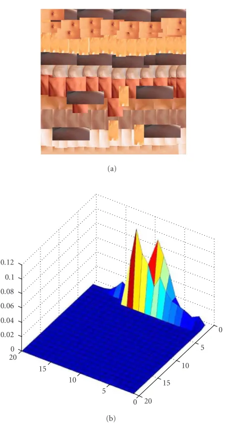
Figure1: (a) Examples of skin tones obtained from various individ-uals with various complexions. (b) The HS histogram model con-structed from picture in (a).
Figure 2: Skin tone segmentation using HS histogram model in Figure 1. Black pixels have been identified.
On-center Off-center
R−G
Figure 3: Color opponent receptive fields in the visual cortex. Unipolar off- and on-cells of G−B andY−B are used to construct
Figure 4: Color opponent computation performed by the chip. Bipolar R−B, R−G, and G−B are used to implement the HSI representation in (1).
color opponents on our chip. Using these color opponents, the RGB-to-HSI conversion is realized.
3. CHIP OVERVIEW
We have designed a 128(H)×64(V)×RGB CMOS imager,
which is integrated with analog and digital signal process-ing circuitry to realize focal plane region-of-interest selec-tion, RGB-to-HSI transformaselec-tion, HSI-based segmentaselec-tion,
36-bin HSI histogramming, and sum-of-absolute-difference
(SAD) template matching for object recognition. This self-contained color imaging and processing chip, designed as a front-end for microrobotics, toys, and “seeing-eye” comput-ers, learns the identity of objects through their color
signa-ture. The signature is composed of a (36bins×12bits)-HSI
histogram template; a minimum intensity and minimum sat-uration filter is employed before histogramming. The tem-plate is stored at the focal plane during a learning step. Dur-ing the recognition step, newly acquired images are com-pared to 32 stored templates using the SAD computer. The minimum SAD result indicates the closest match. In addi-tion, the chip can be used to segment color images and iden-tify regions in the scene having particular color characteris-tics. The location of the matched regions can be used to track
objects in the environment.Figure 5shows a block diagram
XBlock select register XPixel scanning register
Dummy row 1
36,12-b counters (S,I) threshold test (H) decode→36 bins sum-of-absolute differences
Figure5: Computational and physical architecture of the chip.
because the light shielding layer obscures the details). To our knowledge, this is the first chip that integrates imaging, color segmentation, and color-based object recognition at the focal plane.
4. HARDWARE IMPLEMENTATION
4.1. CMOS imaging, white equalization, and normalization
In the imager array, three current values, corresponding to R, G, and B, are sampled and held for each pixel. By storing the color components in this way, a color filter wheel can be used instead of integrated color filters. This step allows us to test the algorithms before migrating to an expensive color CMOS process. When a color CMOS process is used,
the sample-and-hold circuit inFigure 7will be removed. An
R, G, and B triplet per pixel, obtained from on-chip filters,
will then be provided directly to the processing circuit. No change to the scanning or processing circuitry will be required. To facilitate processing, a current mode imaging approach is adopted. It should be noted, however, that current mode imaging is typically noisy. For our targeted ap-plication, the noisiness in the image does not pose a problem and the ease of current mode processing is highly desirable. Current mode imaging also provides more than 120 dB of
dynamic range [10], allows RGB scaling for white correction
using a multiplying DAC and RGB normalization using a
translinear circuit [24]. The normalization guarantees that a
large dynamic range of RGB currents are resized for the HSI transformer to operate correctly. However, it limits the speed of operation to approximately 30 fps because the transistors must operate in subthreshold.
For readout, the pixels can be grouped into blocks of 1×1
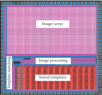
(single pixel) to 128×64 (entire array). The blocks can be
Imager array
T
emplat
e
mat
ching
Image processing
Stored templates
Figure6: Chip layout (light shield layer obscures all details in mi-crograph).
V dd d Sample R Sample G Sample B V dd m
Reset R G B
Row select
(a) V dd m
Scaled R
Intensity
Scaled G Scaled B
I bias
Scaled B Va1 Va1
I bias
B
nor
m
=
I
bias.B/(R
+
G
+
B)
(b)
Figure7: (a) Schematic of the pixel. (b) Schematic of the normal-ization circuit.
Each block is a subimage for which an HSI histogram is con-structed, and can be used as a learned template or a test
tem-plate. The organization of the pixels and the scanning meth-ods are programmable by loading bit patterns in two scan-ning registers, one for scanscan-ning pixels within blocks and the other for scanning the blocks across the array.
Figure 7shows the schematic of the pixel and a portion of the RGB normalizer. The output currents of the pixel are
amplified using tilted mirrors, whereV dd d < V dd m. In
light intensity for which this array is designed, a logarithmic relationship is obtained between light intensity and output
current [25]. Logarithmic transfer functions have also been
observed in biological photoreceptors [26]. This relationship
has the additional benefit of providing wide dynamic range
response. A reset switch is included to accelerate the off
-transition of the pixel. Not shown inFigure 7bis the scaling
circuit that simply multiplies the RGB components by
pro-grammable integer coefficients from 1 to 16. The scaling is
used to white balance the image because silicon photodiodes are more sensitive to red light than to blue.
The normalization circuit computes the ratio of each color component to the sum of the three (i.e., intensity) using
the translinear circuit in Figure 7b. The circuit uses
MOS-FETs operating in subthreshold so that the relationship be-tween the gate-to-source voltages and the currents through
the devices is logarithmic. Hence, the difference of these
volt-ages provides the logarithm of the ratio of currents. By using
the voltage difference as the gate-to-source voltage of another
transistor, a current is produced which is proportional to this ratio (i.e., the anti-log is computed). This function is easily
implemented with the circuit inFigure 7b, however, because
all transistors must operate in subthreshold, that is, with very
small currents on the order of∼1 nA, the circuit can be slow.
Using larger transistors to allow larger bias currents is coun-tered by the increased parasitic capacitance. With a parasitic
capacitance of∼2fF and a bias current of 1nA, a slew rate
of 2µs/V is obtained, while at 30 fps, the circuit needs a time
constant of∼3300/(128×64)=4µs. This circuit limits the
speed of the system to a maximum speed of 30 frames per second despite the relatively small size of the array. In fu-ture designs, this speed problem will be corrected by using an above threshold “normalization” circuit that may not be
as linear as the circuit depicted inFigure 7b.
4.2. RGB-to-HSI conversion
The RGB-to-HSI transformer uses an opponent color
for-mulation, reminiscent of biological color processing [19].
The intensity is obtained before normalization by summing
the RGB components (seeFigure 7b). To compute the
satu-ration of the color, the function in (1b) must be evaluated for
each pixel. Since the minimum of the three normalized com-ponents must be determined, an analog loser-take-all circuit
is used. It is often difficult to implement a loser-take-all, so a
winner-take-all is applied to 1−{r, g, b}. The circuit is shown
inFigure 8. The base winner-take-all circuit is a classical
de-sign presented in [27,28].
For the determination of the Hue of the RGB values, the
function in (1a) must be computed. Since this computation
Sat=I bias (1−min[r, g, b]) V dd m
Figure8: (a) Loser-take-all used for the saturation (S) computa-tion. Actually computes the winner of 1− {r, g, b}. (b) The Hue (H) mixed-signal lookup table.
lookup table. We use a hybrid circuit that simply correlates
the color opponents (g−b), (r−g), and (r−b) to indicate
Hue if the intensity and the saturation of the color are above
a minimum value. The (g−b) and (2r−g−b) components
are each quantized into 16 levels using a 4-bit thermome-ter code analog-to-digital conversion. The lookup table maps
the 16×16 input combinations and the quadrant (as
indi-cated by the two additional sign bits forX andY) into 36
Hue intervals, each having 10 degrees resolution, to cover the 360 degrees of Hue space. The HSI computation is ap-plied to each normalized RGB value scanned from the ar-ray; color segmentation is realized by testing each pixel’s HSI values against prescribed values, and the appropriate label
is applied to the pixel. Figure 8b shows the block diagram
of the Hue computation circuits. Figure 9 shows the
mea-sured normalized currents, rgb, and the color opponents
X = |2r−g−b|andY = |g−b|. The comparison between
theoretical and measuredXandY is also shown. The
vari-ations are expected, given the analog circuits
implementa-tion.Figure 10shows the measured relationship between the
normalizedrgband the computed saturation. The deviation
from the theoretical curve has two components: the diff
er-ence in slope is due to some nonlinearity in the normaliza-tion circuit and a less than unity gain in the saturanormaliza-tion
cir-1
R, G, and B combinations
B norm
R, G, and B combinations
Xmeas Ymeas
Xtheory Y theory (b)
Figure9: (a) shows the normalizedrgbfor various values of RGB. (b) shows the color opponentsX=2 R−G−B andY=G−B.
Figure10: Measured saturation (S) as a function ofrgb.
cuit’s output mirror, while the offset on the right side of the
saturation curve is caused by a layout property that reduced
V dd for one part of the circuit. Consequently, the
satura-tion current is higher than expected when ther component
RGB-to-HSI transformation
0 1 2 3 4 5 6 7 8 9 10 11 12 13 14 15 16 17 18 19 20 21 22 23 24 25 26 27 28 29 30 31 32 33 34 35
360 300 240 180 120 60 0
Theor
etical
H
ue
value
[deg
rees]
0 5 10 15 20 25 30 35
Chip computed Hue bins [10-degree resolution] Figure11: Hue (H) bin assignment for various RGB combinations. The color band shows the input.
Figure 11shows the measured relationship between in-put Hue angle and bin allocation. The plot is obtained by presenting known values of RGB (i.e., Hue angle) to the chip and recording the Hue bins that are triggered. The presentation is done by using the DAC properties of the
RGB scaler circuit (seeFigure 5) with input currents fixed.
This same strategy is used to present the processing core of the chip with images from a PC, as will be shown be-low. There are some overlaps in the response ranges of the individual Hue bins because of imprecision in creating the Hue table’s input addresses. These addresses are created us-ing a simple current ADC that depends on transistor size, gain, and threshold voltage matching. Despite using com-mon centroid layout techniques, we found that the ADC was monotonic but not completely linear. Notice, however, that the overlaps are desirably restricted to the nearest neigh-bor bins. The invariance of the Hue computation to
inten-sity and saturation variations is shown inFigure 12. The
ef-fects of impression in the Hue lookup are again visible in the figure. Nonetheless, this plot shows that the Hue com-putation is insensitive to multiplicative (here intensity varia-tions) and additive shifts (here saturation variavaria-tions), as de-signed.
Next, we tested the color segmentation properties of the chip using real images piped in from a PC. As indicated above, these images are presented by using the RGB scaler circuit as a current DAC. The image of the Rubik’s cube in
Figure 13 demonstrates the effectiveness of our chip on an image containing varying levels of lighting. That is, the fore-ground is well lit, while the backfore-ground is in the shadows. Furthermore, it shows some of the limitations of “wide” Hue interval assigned to every bin. It shows that portions of the image that are highly desaturated or have low intensity can also have similar Hues to other highly saturated and well-lit parts of the image. Using programmable Hue intervals per bin, the transformation lookup table can easily be modified to have finer resolution in targeted portions of the Hue space so that these “similar” Hues can be disambiguated. The next design of this chip will have this capability.
(a)
(b)
Figure12: (a) Measured RGB to Hue transformation as a function of intensity (multiplicative shift). (b) Measured RGB to Hue trans-formation as a function of saturation (additive shift).
(A) (B) (C)
(D) (E) (F)
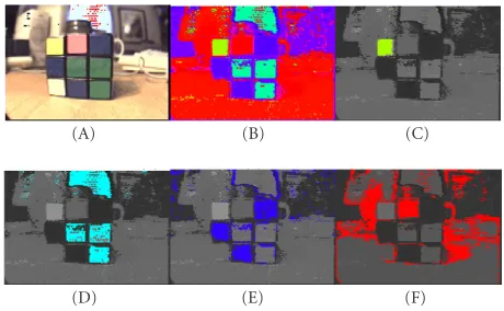
Figure13: Color segmentation on real images. (a) Input image. (b) Complete Hue image. (c) Yellow segment. (d) Cyan segment. (e) Blue segment. (f) One of the red segments.
5. HSI HISTOGRAMMING AND TEMPLATE MATCHING
The HSI histogramming step is performed using 36- and 12-bit counters to measure the number of pixels that fall within each prescribed HSI interval. Here the HSI interval is defined as a minimum intensity value, minimum saturation value, and one of 36 Hue values. In this chip, we count only pixels that pass the intensity and saturation tests. In future versions, we will also count the number of pixels that do not pass the
test.Figure 14shows a block diagram of the histogramming
step. After scanning the imager, the counters hold the color signature of the scene or a portion of the scene (based on
the block selection circuit described inSection 4.1). During
I, S, (G−B), (2R−G−B)
I> λr? N
Y
S> λs? N
Y Analog-to-digital
Hue lookup table
Hue bins
12b-H
u
e(n)
12b-H
u
e(N)
12b bus
Figure14: Block diagram of HSI histogramming.
Figure15: Function of the complete chip: images acquired by the array, learned templates, and locations of matches.
Template matching results 450
400 350 300 250 200 150 100 50 0
SAD
val
ue
1
14 27 40 53 66 79 92 105
Matching threshold
Image segment block index
Figure16: SAD template matching outputs. A threshold of 155 is used to identify the objects inFigure 15.
Figure17: Skin tone identification revisited (using the processing core of the chip). The unimodal Hue distribution of skin leads to some misclassifications.
presented off-chip, where they are sorted using a simple
mi-crocontroller such as a PIC, to find the best match template.
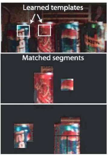
Figure 15shows the whole chip in action, showing the image acquired by the array and blocks identified as templates for “coke” and “pepsi.” Color signatures histograms of the tem-plates constructed, the histograms are stored in the mem-ory and, subsequently, “coke” and “pepsi” are localized in the scene containing multiple cans. The learned segment is
15×15; during matching, the image is scanned in blocks of
15×15, shifted by 8 pixels, for a total of 128 subimages. No
scanned block matches the learned block exactly. A plot of
the SAD error is shown inFigure 16. Match threshold is set
to 155. Notice that the “coke” template also matches part of a pepsi can. This is easily explained by noting that the “coke” only template contains red and white pixels. Hence it matches the part of the pepsi can. On the other hand, the “pepsi” tem-plate contains red, white, and blue pixels. Hence it is not well matched to the other cans and only identifies the pepsi cans.
To further illustrate this point, Figures17and18 show
Figure 18: Fruit identification (using the processing core of the chip). The multimodal distribution of the pineapple eliminates mis-classifications.
both figures, the images were piped through the process-ing core of the chip usprocess-ing the RGB scaler circuit as a DAC. In Figure 17, the task is to identify different skin tones by “learning” templates of various complexions. In all the cases, however, the Hue histogram is a unimodal
distribu-tion, similar to Figure 1b for constant saturation.
Conse-quently, the template matching process misclassifies cloth-ing for skin because the Hue distributions are similar. This misclassifications also happens for single-colored fruits, as
seen in Figure 18. The plums and apples are matched, as
are oranges and peaches. On the other hand, the pineap-ple contains at least two or three bumps in the Hue dis-tribution (blue, green, and yellow). Hence, it can be eas-ily identified and no misclassifications are made. Hence, we can conclude that this method of color-based object
iden-tification is more effective when the target is multicolored.
This conclusion will be exploited in the applications of this
chip. Table 1gives a summary of the characteristics of this
chip.
6. CONCLUSION
The prototype demonstrates that a real-time color segmen-tation and recognition system can be implemented in VLSI using a small silicon area and small power budget. We also demonstrate that the HSI representation used in this chip is robust under multiplicative and additive shift in the origi-nal RGB components. We demonstrate color segmentation
and template matching. Template matching is most effective
when the target is composed of multiple colors. This proto-type was tested using a color filter wheel, where R, G, and B images are sequentially stored in the pixels array. By us-ing a fabrication technology with RGB filters, the entire sys-tem can be realized with a tiny footprint for compact imag-ing/processing applications.
ACKNOWLEDGMENT
This work was supported by National Science Founda-tion (NSF) and Small Business InnovaFounda-tion Research (SBIR)
Table1: Summary of performance.
Technology 0.5µm 3M1P CMOS Array size (R,G,B) 128 (H)×64 (V) Chip area 4.25 mm×4.25 mm Pixel size 24.85µm×24.85µm
Fill factor 20%
FPN ∼5%
Dynamic range >120 db (current mode) Region-of-interest size 1×1 to 128×64 Color current scaling 4 bits
Hue bins 36, each 10 degree wide Saturation Analog (∼5 bits) one threshold Intensity Analog (∼5 bits) one threshold Histogram bin counts 12 bits/bin
Template size 432 bits (12×36 bits) No. stored template 32 (13.8 kbits SRAM) Template matching 4 parallel SAD, 18 bits results
Frame rate Array scan:HSI comp:∼∼30 fps2k fps
Power consumption ∼1 mW at 30 fps on 3.3V supplies
Award (Number DMI-0091594) to Iguana Robotics, Inc. We thank Frank Tejada and Marc Cohen for their help with chip testing.
REFERENCES
[1] O. Yadid-Pecht, R. Ginosar, and Y. S. Diamand, “A random access photodiode array for intelligent image capture,” IEEE Transactions on Electron Devices, vol. 38, no. 8, pp. 1772–1780, 1991.
[2] S. K. Mendis, S. E. Kemeny, and E. R. Fossum, “A 128×128 CMOS active pixel image sensor for highly integrated imaging systems,” inProc. IEEE International Electron Devices Meeting, pp. 583–586, Washington, DC, USA, December 1993. [3] B. Ackland and A. Dickinson, “Camera on a chip,” inProc.
IEEE International Solid-State Circuit Conference, pp. 22–25, San Francisco, Calif, USA, February 1996.
[4] E. R. Fossum, “CMOS image sensors: Electronic camera-on-a-chip,”IEEE Transactions on Electron Devices, vol. 44, no. 10, pp. 1689–1698, 1997.
[5] R. Etienne-Cummings, “Neuromorphic visual motion detec-tion in VLSI,” International Journal of Computer Vision, vol. 44, no. 3, pp. 175–198, 2001.
[6] R. Etienne-Cummings, Z. Kalayijan, and D. Cai, “A pro-grammable focal-plane MIMD image processor chip,” IEEE Journal of Solid-State Circuits, vol. 36, no. 1, pp. 64–73, 2001. [7] K. Yoon, C. Kim, B. Lee, and D. Lee, “Single-chip CMOS
im-age sensor for mobile application,”ISSCC 2002 Digest of Tech-nical Papers, vol. 45, pp. 36–37, 2002.
Trans. Circuits and Systems for Video Technology, vol. 2, no. 4, pp. 392–400, 1992.
[9] T. Sugiyama, S. Yoshimura, R. Suzuki, and H. Sumi, “A 1/4-inch QVGA color imaging and 3D sensing CMOS and analog frame memory,” ISSCC 2002 Digest of Technical Papers, vol. 45, pp. 434–435, 2002.
[10] C. Mead, “Sensitive electronic photoreceptor,” inProc. 1985 Chapel Hill Conference on VLSI, pp. 463–471, Computer Sci-ence Press, Rockville, Md, USA, 1985.
[11] C. Mead and M. Ismail, Eds., Analog VLSI Implementation of Neural Networks, Kluwer Academic Press, Norwell, Mass, USA, 1989.
[12] H. Barlow, The Senses: Physiology of the Retina, Cambridge University Press, Cambridge, UK, 1982.
[13] C. Mead, “Neuromorphic electronic systems,” Proceedings of the IEEE, vol. 78, no. 10, pp. 1629–1636, 1990.
[14] C. Koch and H. Li, Vision Chips: Implementing Vision Algo-rithms with Analog VLSI Circuits, IEEE Computer Society Press, Los Alamitos, Calif, USA, 1995.
[15] V. Brajovic and T. Kanade, “Computational sensor for visual tracking with attention,” IEEE Journal of Solid-State Circuits, vol. 33, no. 8, pp. 1199–1207, 1998.
[16] A. Zarandy, M. Csapodi, and T. Roska, “20µsec focal plane image processing,” inProc. 6th IEEE International Workshop on Cellular Neural Networks and Their Applications, pp. 267– 271, Catania, Italy, 2000.
[17] M. Loinaz, K. Singh, A. Blanksby, D. Inglis, K. Azadet, and B. Ackland, “A 200-mW, 3.3-V, CMOS color camera IC pro-ducing 352×288 24-B video at 30 frames/s,”IEEE Journal of Solid-State Circuits, vol. 33, no. 12, pp. 2092–2103, 1998. [18] A. Moore, J. Allman, and R. Goodman, “A real-time neural
system for color constancy,”IEEE Transactions on Neural Net-works, vol. 2, no. 2, pp. 237–247, 1991.
[19] F. Perez and C. Koch, “Towards color image segmentation in analog VLSI: algorithms and hardware,”International Journal of Computer Vision, vol. 12, no. 1, pp. 17–42, 1994.
[20] K. Tanaka, “Inferotemporal cortex and object vision,”Annual Review of Neuroscience, vol. 19, no. 1, pp. 109–139, 1996. [21] E. Rolls, “Functions of the primate temporal lobe cortical
visual areas in invariant visual object and face recognition,” Neuron, vol. 27, pp. 205–218, 2000.
[22] R. Gonzalez and R. Woods,Digital Image Processing, Addison-Wesley, Reading, Mass, USA, 1992.
[23] E. Kandel, J. Schwartz, and T. Jessell,Principles of Neural Sci-ence, McGraw-Hill, New York, NY, USA, 4th edition, 2000. [24] B. Gilbert, “Translinear circuits—25 years on part I. The
foundations,”Electronic Engineering, vol. 65, no. 800, pp. 21– 24, 1993.
[25] V. Gruev and R. Etienne-Cummings, “Implementation of steerable spatiotemporal image filters on the focal plane,” to appear in IEEE Trans. Circuits and Systems-II.
[26] R. Normann and F. Werblin, “Control of retinal sensitivity. I. Light and dark adaptation of vertebrate rods and cones,”J. General Physiology, vol. 63, no. 1, pp. 37–61, 1974.
[27] J. Lazzaro and C. Mead, “A silicon model of auditory localiza-tion,”Neural Computation, vol. 1, no. 1, pp. 41–70, 1989. [28] G. Indiveri, “A current-mode analog hysteretic
winner-take-all network, with excitatory and inhibitory coupling,” Ana-log Integrated Circuits and Signal Processing, vol. 28, no. 3, pp. 279–291, 2001.
Ralph Etienne-Cummingsreceived his B.S. degree in physics, 1988, from Lincoln Uni-versity, Pennsylvania, and completed his M.S.E.E. and Ph.D. degrees in electrical en-gineering at the University of Pennsylva-nia in 1991 and 1994, respectively. Cur-rently, Dr. Etienne-Cummings is an Asso-ciate Professor of computer engineering at Johns Hopkins University (JHU), on leave from the University of Maryland, College
Park (UMCP). He is also Director of computer engineering at JHU and the Institute of Neuromorphic Engineering (currently admin-istered by UMCP). He is the recipient of the NSF’s Career and ONR YIP Awards. His research interest includes mixed signal VLSI sys-tems, computational sensors, computer vision, neuromorphic en-gineering, smart structures, mobile robotics, and legged locomo-tion.
Philippe Pouliquenreceived his B.S.E. de-gree in biomedical engineering and his M.S.E. degree in electrical and computer engineering from the Johns Hopkins Uni-versity in 1990, and his Ph.D. degree in electrical and computer engineering from the Johns Hopkins University in 1997. Dr. Pouliquen has served as a Consultant to the US Army NVESD since 1996, as Senior Design Engineer for Iguana Robotics, Inc.
since 1999, and as CEO of Padgett-Martin Technology, Inc. from 1999 to 2000. He has also been pursuing research in SOS optoelec-tronic circuits and CMOS analog VLSI circuits including current references ADCs, DACs, and low-power digital circuits.
M. Anthony Lewisreceived his B.S. degree in cybernetics from the University of Cali-fornia, Los Angeles, and his M.S. and Ph.D. degrees in electrical engineering from the University of Southern California. His re-search areas include learning in legged lo-comotion, computational models of visuo-motor behavior, and embedded visual algo-rithms. He began his career in robotics at Hughes Aircraft building snake-like robot