ABSTRACT
MALHOTRA, ABHISHEK. Thermoelectric Generators for Wearable Application: Materials and Devices. (Under the supervision of Dr. Daryoosh Vashaee).
Thermoelectric generators are devices that can be used to harvest body heat and produce electricity. They are promising candidates for making battery-less wearable systems. Several challenges must be addressed before TEGs can power wearables in real life. Bi-Sb-Te-Se nanocomposite alloys are known as state-of-the-art thermoelectric materials for near room-temperature applications; however, the existing materials often have their peak efficiency in the temperature range of 100 oC to 150 oC. Additionally, these nanocomposites often suffer from a lack of reproducibility due to the difficulties in controlling the lattice defects during the material synthesis process. Another essential element imposed by the low-temperature differential between the body and the environment is related to requiring thin and long TE legs and low fill factor devices. This work will describe methods to address some of these issues, starting from material synthesis, device design, and TEG fabrication to integration in wearable testbeds.
In this Ph.D. research, an extensive investigation was performed on the doping optimization and reproducibility of n-type materials. The effects of Cu doping for synthesizing a
Alternately, the experimental thermoelectric realization of Bi-Te-S compound was evaluated via mixing the Bi2Te3 and Bi2S3 alloys. The introduction of sulfur caused a decrease in
electrical conductivities. Also, it increased the Seebeck coefficient mostly because of a reduction in the carrier concentration (n) by replacing Te with S in the crystal structure. Moreover, the heterostructure of the alloy provided a reduction in thermal conductivity. The maximum zT values were calculated to be about 0.7 at a temperature of 140 °C for the undoped alloy and 0.72 at a temperature of 70 °C for the doped alloy. These results contrast the Bergman theory of classical composites [1]. The enhancement suggests non-equilibrium spectra of the charge carriers in the Bi2Te3-Bi2Te2S nanocomposite material.
This work will also discuss an alternative, microwave (MW) sintering method that can produce nanostructured bulk compounds with excellent thermoelectric properties compared to conventional methods. This is a two-step process involving a uniform mixing of the elements and subsequent MW radiation. The synthesis occurs at a temperature lower than the melting point, which in turn lowers the overall power requirement. Furthermore, the
Thermoelectric Generators for Wearable Application: Materials and Devices
by
Abhishek Malhotra
A dissertation submitted to the Graduate Faculty of North Carolina State University
in partial fulfillment of the requirements for the degree of
Doctor of Philosophy
Electrical Engineering
Raleigh, North Carolina 2019
APPROVED BY:
_______________________________ _______________________________ Dr. Daryoosh Vashaee Dr. Veena Misra
Committee Chair
_______________________________ _______________________________ Dr. Mehmet C. Öztürk Dr. Lewis Reynolds Jr.
ii DEDICATION
I dedicate this thesis to my parents Kiran and Ashok Malhotra, and my sister Aakriti Malhotra.
iii BIOGRAPHYaa
iv TABLE OF CONTENTS
LIST OF TABLES……….. ... vi
LIST OF FIGURES ... vii
Chapter 1: Introduction ... 1
1.1 Thermoelectric Fundamentals ... 1
1.1.1 The Three Thermoelectric Effects ... 1
1.1.2 The efficiency of Thermoelectric Materials ... 2
1.1.3 Bi-Te alloys ... 4
1.2 Challenges of thermoelectric for wearable application ... 8
1.2.1 Peak zT at room temperature ... 8
1.2.2 zT is Not Everything for Body Heat Harvesting ... 8
1.2.3 Bipolar Effect ... 9
1.3 Recent Methods to improve zT at room temperature ... 10
1.3.1 Nano-structuring ... 10
1.3.2 Nanocomposites ... 11
1.3.3 Microwave sintering ... 11
1.3.4 Structure of this thesis ... 12
Chapter 2: Methodologies and Characterization ... 14
2.1 Introduction ... 14
2.2 Melt-Quench Annealing ... 14
2.3 Milling ... 16
2.4 Spark Plasma Sintering ... 17
2.5 Microwave Sintering ... 19
2.6 X-ray Diffraction ... 21
2.7 Electronic Properties ... 21
2.8 Thermal Diffusivity ... 22
Chapter 3: Bi2Te3-xSex Thermoelectric Study Using Microwave Sintering for Room Temperature Application ... 24
3.1 Introduction ... 24
3.2 Materials and methods ... 26
3.3 Results and Discussion ... 27
3.4 Conclusion ... 31
v
4.1 Introduction ... 33
4.2 Materials and Methods ... 35
4.3 Results and discussion ... 36
4.4 Conclusion ... 42
Chapter 5: Experimental Synthesis and Thermoelectric Characterization of Bi-Te-S Compound…. ... 44
5.1 Introduction ... 44
5.2 Materials and method ... 45
5.3 Results and discussion ... 46
5.4 Conclusions ... 51
Chapter 6: Thermoelectric Generator Device Fabrication ... 52
6.1 Introduction ... 52
6.2 Design and Methodology ... 53
6.2.1 TEG Design ... 53
6.2.2 Sample preparation ... 54
6.2.3 Dicing, Surface preparation, and Metallization ... 56
6.2.4 Leg dicing ... 63
6.2.5 Leg cleaning and separation... 64
6.2.6 Bonder System ... 65
6.2.7 Bonder Upgrades for Improved Throughput ... 66
6.2.8 Device Fabrication ... 68
6.3 Characterization of Modular TEG... 73
6.4 Conclusion ... 76
Chapter 7: Rapid Solid-State Reaction and Simultaneous Sintering of Thermoelectric Compounds under Microwave Radiation ... 77
7.1 Introduction ... 77
7.2 Materials and methods ... 78
7.3 Results and Discussion ... 80
7.3.1 Bi0.5Sb1.5Te3 ... 80
7.3.2 Microwave synthesis of other thermoelectric compounds ... 83
7.4 Conclusion ... 86
Chapter 8: Conclusion and Future Work ... 88
8.1. Conclusion ... 88
8.2. Future Work ... 90
vi LIST OF TABLES
Table 1.1: Electronic and Thermodynamic data for Te, Se, Bi, and Sb. ... 5
Table 1.2: Peak zT values in literature with their corresponding thermal conductivity and temperature. ... 8
Table 3.1: Atomic composition of x= 0.3 and 0.8 before and after CMW sintering. It is observed that the post MW sample for Se0.3 has lost Te, which can be attributed to Te loss during the process. ... 31
Table 4.1: Comparison of room temperature properties of this study and other studies on n-type Bi2Te3. ... 41
Table 4.2: Comparison of TEGs made with nanocomposite and commercial legs. ... 42
Table 6.1: Design parameters for a single TEG. ... 53
Table 6.2: AC resistance of the 9 TEGs used in making the modular TEG. ... 74
Table 6.3: Input and output power of the TEG using the Mercury boost converter. ... 76
vii LIST OF FIGURES
Figure 1.1: Thermoelectric properties vs. charge carriers for an arbitrary thermoelectric material. ... 3 Figure 1.2: The Seebeck coefficient which is +ve for p-type and -ve for n-type materials
as a function of initial Te concentration. ... 6 Figure 1.3: Unit cell of a Bi2Te3-Sb2Te3 isomorphous solution. ... 7
Figure 1.4: Unit cell of a Bi2Te3-Bi2Se3 isomorphous solution. ... 7
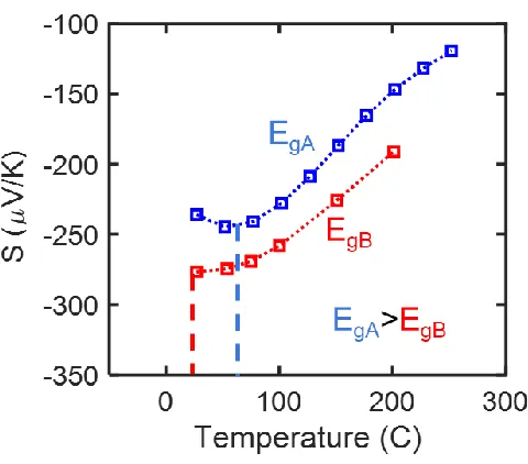
Figure 1.5: Comparison of Seebeck of similar materials with different bandgaps. The
onset of the bipolar effect is delayed for the material with the larger bandgap. . 10 Figure 2.1: a) Melting process of material in a quartz tube under an acetylene torch. b)
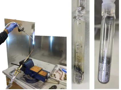
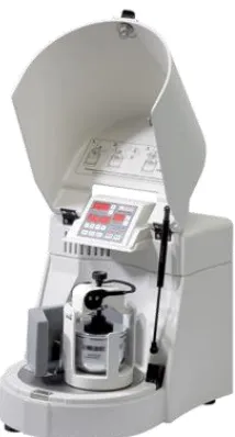
Melted alloy starting from elemental powders. c) Melted alloy starting from elemental chunks. ... 16 Figure 2.2: A Planetary Mono Mill PULVERISETTE 6 used for nanostructuring of
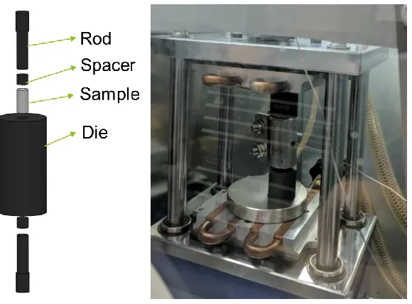
materials. ... 17 Figure 2.3: a) Typical die setup for hot-pressing. b) Custom hot press system installed in a
glovebox with an argon environment. ... 19 Figure 2.4: MW system used for sintering thermoelectric materials. ... 21 Figure 3.1: Comparison of electronic properties of Bi2Te3-xSez samples at room
temperature for x=0.1 to 0.9 at room temperature. The dashed lines represent samples before MW sintering, and the solid lines represent samples after MW sintering. The x-axis represents the samples with different Se concentration. The black, red and blue curves represent the Seebeck coefficient, electrical conductivity and the power factor respectively ... 28 Figure 3.2: On the left is the thermal conductivity data for all the samples after MW
sintering. The sample with Se=0.6 has the lowest thermal conductivity, and the sample with Se=0.2 has the highest thermal conductivity at room
temperature. The figure on the right is zT for all the samples. The sample with Se=0.3 has the highest zT of 0.82 at around room temperature. ... 29 Figure 3.3: Thermoelectric properties of a sample with Se=0.3 before and after microwave
sintering. ... 30 Figure 4.1: Crystal structure of Bi2Te3 consisting of repeating chains of -Te-Bi-Te-Te-
Bi-Te-. The Te2 atom can be dislodged from its position resulting in a
tellurium vacancy (VTe) and 2 free electrons. ... 34
Figure 4.2: Electronic properties of 7 samples of Bi2Te2.7Se0.3 processed using ball milling
and SPS under similar conditions. ... 36 Figure 4.3: Electronic properties of Bi2Te2.8Se0.2 doped with different copper
concentrations. ... 37 Figure 4.4: Room temperature data for different Cu doping and SPS temperature and
their effects on a) Seebeck, b) electrical conductivity and c) power factor of Bi2Te2.8Se0.2. The peak power factor is for a copper concentration of 0.01875. . 38
viii higher power factor compared to the undoped sample. b)The 9 samples used for this reproducibility study. ... 39 Figure 4.6: a) Thermal conductivity, b) zT values of Bi2Te2.8Se0.2Cu0.01875 alloy (black line)40
Figure 4.7: a) Characterization setup of the device. The hotplate is set to 33C to mimic skin temperature. b) Images of TEGs with 48 legs. ... 42 Figure 5.1: Phase diagram of Bi-Te-S alloy. ... 45 Figure 5.2: XRD analysis of the 5 different compositions of the Bi-Te-S system showing
two separate phases Bi2Te3 and Bi2Te2S1. ... 47
Figure 5.3: Thermoelectric properties of Bi-Te-S alloys of different compositions. Peak zT was found for the sample with S=0.25. ... 48 Figure 5.4: Thermoelectric properties of samples with S=0.5 and 0.15 with different
Iodine doping levels. ... 50 Figure 6.1: Top and bottom header with metal pads along with a scaled drawing of a
device. ... 54 Figure 6.2: Statistical data for the final 9 p-type samples used for device preparation. ... 55 Figure 6.3: Thermoelectric properties for sample 238 which was hot-pressed at 540C for
15mins ... 55 Figure 6.4: The 9 p-type samples used for preparing devices. ... 56 Figure 6.5: N and P-type discs after dicing and cleaning. ... 56 Figure 6.6: 6 n-type (top) and 6 p-type (bottom) samples loaded on a 4" silicon wafer
using double-sided Kapton tape. The physical etch numbers represent
sandpaper grit size. ... 58 Figure 6.7: IR images of the top of the device. Hot spots indicate poor contact resistance. .. 59 Figure 6.8: SEM analysis of an n-type leg. ... 60 Figure 6.9: Sandblaster loaded with 15um Alumina particles. ... 61 Figure 6.10: 4 p-type (top) and 10 n-type (bottom) samples loaded on a 4" silicon wafer
using double-sided Kapton tape. The sandpaper numbers represent grit size. .... 62 Figure 6.11: All p-type (top two rows) and n-type (bottom two rows) discs loaded on a 4"
silicon wafer sputtered on both sides. ... 63 Figure 6.12: a) Graphite mold with 9 wells machined using an end-mill. b) Molds filled
with discs and covered with wax to support the discs during dicing. c) Mold after first set cuts, covered with JB weld epoxy to support the second set of cuts. d) Mold after both sets of cuts. ... 64 Figure 6.13: On the left are cleaned legs transferred to a petri dish after inspection. On the
right is a closeup of the legs. ... 65 Figure 6.14: Device bonder system with the various alignment locations for calibration. .... 66 Figure 6.15: Leg getting stuck in stencil during release. ... 67 Figure 6.16: Vacuum chuck drawing with custom well design for placing legs (left).
Schematic of legs being released after reflow soldering (right). ... 68 Figure 6.17: (left)Vacuum chuck loaded with alternating n and p legs. (middle) Test
ix
Figure 6.19: Larger bottom header imprinted with solder in a 3x3 pattern. ... 70
Figure 6.20: Modular TEG without top header with 9 TEGs soldered to the bottom header. 70 Figure 6.21: Three different conductive fabrics tested for textiles integration. The fibers use copper, carbon nanotubes, and nickel (left to right) as the conductive material. ... 71
Figure 6.22: Test device using brass plates and nickel conductive fibers. ... 72
Figure 6.23: Final modular TEG integrated with conductive fabric. ... 72
Figure 6.24: Modular TEG integrated with a vest utilizing metal snaps. ... 73
Figure 6.25: Measurement setup for characterizing modular TEG. Airflow was generated with a desk fan and calibrated with a digital anemometer. ... 74
Figure 6.26: Comparison of efficiency for 3 different boost converters vs. air velocity and input voltage. ... 75
Figure 7.1: Schematic of single-mode MW system used for all experiments. ... 79
Figure 7.2: Microwave heating profile of a typical sample up to 375 °C. ... 80
Figure 7.3: a) XRD data of the initially milled powder and samples consolidated using MW sintering at 350, 400 and 425 oC, b) Microwave sintered bulk sample with 99% density. ... 81
Figure 7.4: a) XRD patterns for three different MW temperatures and b) Thermal conductivities of sintered Bi0.5Sb1.5Te3 samples. ... 82
Figure 7.5: TEM image of Bi0.5Sb1.5Te3 sample sintered at 400 °C. ... 83
Figure 7.6: XRD data of Sb2Te3 elemental powder compared to powder sintered at 3 different temperatures- 375°C, 400°C, and 425°C. The figure on the right highlights the changes in the composition with increasing sintering temperatures. ... 84
Figure 7.7: XRD analysis of Cr-Sb study with a comparison of mixed powder with samples sintered at 650, 750, 850, and 950 °C. ... 85
Figure 7.8: Comparison of relative peak intensities of Sb (012) and CrSb (101) vs. microwave sintering temperature. ... 86
1
Chapter 1:
Introduction
Wearable technology shows great promise in the fields of medicine, patient care, and chronic disease research. With the advancement of sensors for environmental and
physiological markers, it is possible to track a person’s environment continuously. This can provide great insight for doctors to keep track of patients and for scientists studying various chronic ailments but lack enough data to correlate this information. Decreasing power requirements for wearable sensors [2][3][4][5] and system-on-chip [6][7][8] provides an opportunity to design wearable systems for different applications that can monitor these parameters. However, there is a gap in the energy generation necessary for sensors
continuously. This work is focused on advancing the field of thermoelectric harvesting for the wearable application of both materials and devices. The motivation is to explore different materials and processes specifically to improve the performance at room temperature and to design and optimize a method for fabricating thermoelectric generators (TEG) with the flexibility to make changes to the geometry of them for the application of continuous monitoring wearable systems.
1.1Thermoelectric Fundamentals
1.1.1 The Three Thermoelectric Effects
2 value known as the Seebeck coefficient, which is a material property. This effect is used for energy harvesting applications in the presence of a temperature difference. The Peltier effect is essentially the reverse of this effect, where when a current passed through a material result in a generation of a temperature difference across the material. The ratio of the heat flux through the material to the current applied to the material is a constant known as the Peltier coefficient, which is also a material property. This effect is generally used for refrigeration or heating applications. William Thomson first derived a relation between the Seebeck
coefficient and the Peltier coefficient. His theory resulted in a third thermoelectric theory called the Thomson effect, where a current flown through a temperature gradient can cause heating or cooling because of the charge carriers transferring the heat.
1.1.2 The efficiency of Thermoelectric Materials
The efficiency (η) of a thermoelectric device is given as
η =TH− TC
TH ×
√(1 + ZT) − 1
√(1 + ZT) + TC
TH
( 1)
Where ZT is the dimensionless figure of merit of the device, and TH and TC are temperatures
of the hot and cold side, respectively. The term (TH-TC)/TH is the expression for the Carnot
efficiency of a system. Typically, ZT represents the figure of merit for a device, whereas zT represents the figure of merit of the material. zT is always higher than ZT for a device due to resistive losses at the contacts in a device. zT is represented as
zT = σS
2
3 Where σ is the electrical conductivity, S is the Seebeck coefficient, κ is the thermal
conductivity, and T is the absolute temperature. The challenge to improve the efficiency of thermoelectric materials comes from the fact that all the components of z are coupled. An increase in electrical conductivity generally results in a decrease in Seebeck and an increase in thermal conductivity. Figure 1.1 perfectly illustrates the challenge of optimizing these materials. The peak zT does not correspond with the peak of any of its individual
constituents.
Figure 1.1: Thermoelectric properties vs. charge carriers for an arbitrary thermoelectric material [9].
Traditionally there are three families of materials that cover three temperature ranges, namely Bi-Te for low temp, Pb-Te for mid-range, and Si-Ge for high temp. This work is focused on low-temperature applications, and the material explored is Bi-Te alloys. The next section discusses this material in detail.
4 1.1.3 Bi-Te alloys
Bismuth Telluride and its alloys are the most common thermoelectric material for room temperature energy harvesting. They form a hexagonal crystal structure that consists of a chain of Bi and Te atoms. Bi-Te2 and Bi-Te1 form ionic bonds, whereas the Te1-Te1
consists of Van der Waals bonds [10].
−Te1− Bi − Te2− Bi − Te1−
This results in a large anisotropy in the mechanical and electronic properties of the material. Due to this anisotropy in mechanical properties, these materials are used in
polycrystalline form for bulk applications. Even though the polycrystallinity results in lower electrical properties, the resulting mechanical strength is instrumental in manufacturing robust thermoelectric generators. A solid solution of Bi2Te3 with its isomorph Sb2Te3 results
in the same hexagonal crystal structure with Sb displacing Bi atoms. The resulting composite (Bi1-xSbx)2Te3 is p-type for x>0.510. The advantage of using composite materials over doping
Bi2Te3 with p-type dopants is the reduction of thermal conductivity and a delay in the bipolar
effect because of the larger bandgap of this composite.
Similarly, Bi2Te3 and its isomorph Bi2Se3 are combined to make n-type material. The
Se displaces the Te2 first because of its higher electronegativity. This results in an increase in the bandgap in which is favorable for room temperature applications.
Bi2Te3 is a defect doped semiconductor which can be either p-type or n-type
5 occur in different properties, and defect management is vital to growing materials with
reproducible properties.
Table 1.1: Electronic and Thermodynamic data for Te, Se, Bi, and Sb [11].
Te Se Bi Sb
Evaporation heat (kJ/mol) 52.55 37.7 104.8 77.14
Electronegativity 2.1 2.55 2.02 2.05
Covalent radius (A) 127.6 78.96 208.98 121.75
When bismuth telluride crystal is grown utilizing a zone melting technique, the final stoichiometry inevitably contains excess Bi. This occurs because Te has a very low
evaporation of heat, as shown in table 1. This results in a VTe which has 2+ vacancy and 2 e-s
[12].
TeTe → Te(g) ↑ +VTe∗∗ + 2e−
Due to the similar electronegativity, the Bi ions to Te ions (Table 1.1) can occupy this vacancy resulting in an anti-site defect. This anti-site defect is what causes grown crystalline Bi2Te3 to form a p-type material. The BiTe creates a total of 4 holes, which compensates the 2
e-s created by the VTe [12].
BiBi+ VTe∗∗ + 2e− → V
Bi′′′+ BiTe′ + 4p+
This VTe and BiTe can be controlled by varying the initial concentrations of Bi and Te.
Beginning with excess Te can result in lowering of the VTe and may also result in TeBi which
6 Figure 1.2: The Seebeck coefficient, which is +ve for p-type and -ve for n-type materials as a
function of initial Te concentration [13].
This method of doping is highly sensitive to the initial conditions and can be
challenging to control. An alternative way to dope Bi2Te3 is through substitutional doping.
7 For p-type semiconductor, a solution of Bi2Te3-Sb2Te3 is made with 75% Sb2Te3
being the optimal ratio for the lowest lattice thermal conductivity [10]. The Sb occupies the Bi site in the lattice, as represented in Figure 1.3.
Figure 1.3: Unit cell of a Bi2Te3-Sb2Te3 isomorphous solution.
Due to the closer electronegativity to Te, this results in a higher number of SbTe
defects, which makes the material strongly p-type [10]. The doping mechanisms are like Bi2Te3. Similarly, for n-type semiconductors, an isomorphous solution of Bi2Te3-Bi2Se3 is
used. The unit cell of this solution is illustrated in Figure 1.4. Due to its higher
electronegativity, Se first occupies the Te2 position in the lattice as it results in an overall
lowering of the system energy [10].
Figure 1.4: Unit cell of a Bi2Te3-Bi2Se3 isomorphous solution.
Another consequence of this higher electronegativity is an increase in the bandgap of the material [15] - which is a desirable effect for thermoelectric materials. Once all the Te2 positions are occupied, the Se starts filling Te1 positions [15]. This results in the lowering of the bandgap. The Se addition reduces the BiTe due to a stronger bond with Bi. Because there
8 1.2Challenges of thermoelectric for wearable application
1.2.1 Peak zT at room temperature
Table 1.2 represents some of the best n-type materials in literature for
low-temperature energy harvesting. The key trend to notice here is the low-temperature of their peak efficiency. None of the materials have been optimized for room temperature application. This implies that there is a gap in the space of wearable applications, which has to be fulfilled to achieve state of the art self-powered wearable devices.
Table 1.2: Peak zT values in literature with their corresponding thermal conductivity and temperature.
Composition κ(W/m/K) zT T (°C) Ref. 1 Bi2Te2.7Se0.3 1.15 1.04 125 [16]
2 Bi2Te2.79Se0.21 1.0 1.2 85 [17]
3 Bi2Te2.3Se0.7 1.2 1.2 170 [18]
4 Cu0.01Bi2Te2.7Se0.3 1.1 1.1 125 [19]
5 Bi2Te2.7Se0.3 0.8 1.1 100 [20]
6 Bi2Te2.7Se0.3 0.75 1.23 205 [21]
7 Bi2(TeSe)3 1.1 1.1 200 [22]
8 Bi2Te2.4Se0.6 1.5 1.22 205 [23]
9 Bi2Te2.7Se0.3 1.7 1.1 210 [24]
1.2.2 zT is Not Everything for Body Heat Harvesting
9 30% more power than a material with zT of 2 and k of 1.5. These are startling results and are considered during the material synthesis and device fabrication in this work.
TEGs when used for a wearable application, must be connected to a boost converter to power the various parts of smart devices. This is because practical TEGs can only generate a voltage in the mV for the small temperature difference available in the wearable
application. Since the efficiency of boost converters is proportional to the input voltage, using materials with larger Seebeck can have greater benefits even if the power factor is sacrificed in this process. A combination of low thermal conductivity and high Seebeck are hence essential for a good TEG for body heat application.
1.2.3 Bipolar Effect
The bipolar effect is the generation of electron-hole pairs in a semiconductor material resulting in minority charge carriers. These pairs move from the hot side to the cold side under a temperature gradient, and the net current is zero. Since electrons and holes have opposite signs; however, the Seebeck coefficient can be significantly affected [26]. And since the charged pairs carry heat, this can lead to an increase in thermal conductivity. This implies that reducing bipolar contribution can result in a double benefit to improve the zT of a
material. The onset of the bipolar effect can be controlled by engineering the bandgap of material, as seen in Figure 1.5. As mentioned earlier, the bandgap of Bi2Te3 can be modified
by creating solutions with Sb2Te3 and Bi2Se3. The ratios of these alloys can be controlled to
10 Figure 1.5: Comparison of Seebeck of similar materials with different bandgaps. The onset of
the bipolar effect is delayed for the material with the larger bandgap. 1.3Recent Methods to improve zT at room temperature
1.3.1 Nano-structuring
11 1.3.2 Nanocomposites
Nanocomposites are a broad range of materials that have shown to improve zT with different nano-scale features [37]. They typically consist of 2 or more different alloy systems, such as Bi2Te3/Sb2Te3, PbTe/ Sb2Te3, SiGe/CrSi2, etc. When combined with grain boundary
phases, lamellar structures, dendrite structure, precipitates, and nanoinclusions[9], significant enhancements can be seen in thermoelectric properties [38][39][40][41]. Nanocomposites typically start with nanopowders, which are consolidated into samples using spark plasma sintering. When compared to single-crystal structures of their constituents, nanocomposites show a higher power factor and lower thermal conductivity. By optimizing doping levels in these constituents, it is possible to tune properties to the desired temperature application.
1.3.3 Microwave sintering
Microwave radiation has been traditionally used for its uniform heating properties. This heating takes place due to the interaction of microwaves with dipoles in a material. Due to the oscillating field, the interaction results in the heating of the material because of
12 processing time. Also, this process can be applied to already sintered samples, which
eliminates processing steps like SPS, which typically result in grain growth. If combined with other effects such as densification and accelerated diffusion, it is possible to in-situ synthesize and decrystallize thermoelectric materials without the need for additional steps. Therefore, microwave sintering is a promising method for future improvements in
thermoelectric properties and a candidate for synthesizing materials in the industry due to its time and energy-saving characteristics.
1.3.4 Structure of this thesis
This research is focused on the synthesis of thermoelectric materials for body heat harvesting. Chapter 1 covers the background for this work. With the improvements in energy harvesting and the increase in low powered sensors, it is possible to power these sensors indefinitely using body heat. However, the current state-of-the-art thermoelectric generators are not optimized for room temperature. This creates a gap, which is something this work tries to fill. Different methods, standard and new, to improve the efficiency of thermoelectric materials are also discussed in chapter 1.
In Chapter 2, the general methods used for the synthesis and characterization of thermoelectric materials is discussed. These methods are used in a different combination in the following experiments to synthesize materials.
13 In Chapter 4, the result of the previous study is used to synthesize n-type Bi-Te-Se for wearable applications. The reproducibility issues are discussed in this study. The effect of Cu-doping on the thermoelectric properties is studied as well.
In Chapter 5, a new method for synthesizing thermoelectric materials is discussed. This method is used with Bi-Te-S alloys, and a systematic study is performed for the same. This study was also collaborative.
In Chapter 6, a process flow for dicing samples, metallization, dicing legs, bonding TEG devices, and textiles integration is discussed.
In Chapter 7, a novel process for synthesizing and sintering thermoelectric materials is presented. Bi-Sb-Te, Bi-Te, Sb-Te, Cr-Sb, and Mn-Te are synthesized using microwave processing. The rabid synthesis process is discussed, and a model is provided to understand rapid densification under microwave radiation. This study was a collaborative work.
14
Chapter 2:
Methodologies and Characterization
2.1Introduction
The following sections describe the steps used to synthesize and characterize materials. Different experiments need different combinations of these steps, but in general, the operations involve - material synthesis, sample consolidation, characterization, and repetition based on the characterization results.
2.2Melt-Quench Annealing
15 and result in a random stoichiometry. Once a good seal is formed, the ampule is left to cool down naturally. Next, the acetylene torch is set to a reducing flame since we do not need to and want to melt the quartz anymore. The ampule is slowly introduced into the flame and shaken over the flame. As the powders start melting, the ampule is lowered until the melt is molten orange. This is then shaken vigorously for a few minutes before it is quenched in a bath of cold water. Next, the ampule is transferred to the oven where it is annealed for 2.5 to 3 days at 210C.
It is essential to note the comparison of ampules for powders vs. chunks, as seen in Figure 2.1. Due to a larger surface area, any oxidation of elemental powders can result in a more considerable amount of contamination. And since the amount of oxidized powder isn’t known, it can result in discrepancies in the stoichiometry of the final alloy. This issue can be minimized by using elemental chunks. Since the surface area to volume ratio is much
16 Figure 2.1: a) Melting process of material in a quartz tube under an acetylene torch. b) Melted alloy starting from elemental powders. c) Melted alloy starting from elemental
chunks. 2.3Milling
Once the annealing is complete, the ampule is transferred to the glovebox, where the ingot is extracted for the mechanical milling step. The Planetary Mono Mill
17 of 8hours of milling. After the milling, the cup is transferred to the glovebox. The contents are sieved to separate the powders and the Zirconia balls. This powder is then used for the next steps.
Figure 2.2: A Planetary Mono Mill PULVERISETTE 6 used for nanostructuring of materials. 2.4Spark Plasma Sintering
18 radiative heat loss. This gives us more control over the temperature profile and results in a lower current for the same operation. The die with the insulating fabric is encapsulated in a steel clamp. This clamp keeps the fabric in place and prevents debris from flying around in case of mechanical failure of the die. After loading, the spacers are inserted followed by rods. Next, this is cold-pressed up to 150psi. This reduces the chance of loss of contact when the powder softens during the hot pressing. Once, cold-pressed, the K-Type thermocouple is inserted into a cavity pre-drilled into the graphite die.
19 Figure 2.3: a) Typical die setup for hot-pressing. b) Custom hot press system installed in a
glovebox with an argon environment. 2.5Microwave Sintering
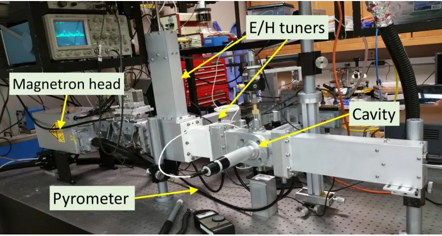
Microwave (MW) sintering involves the exposure of a hot-pressed or cold-pressed sample to MW radiation. The setup consists of an MW source, a magnetron for our setup, a sliding short to control the length of the cavity, and 2 tuners to control the E and H field. The MW system used in our lab is depicted in Figure 2.4. The sliding short and tuners are tuned to form a high-quality factor standing wave inside the cavity. The tuning must be varied throughout the experiment due to the changing absorption properties of materials with respect to temperature. The sample is first loaded in a Boron Nitride (BN) die. BN acts as a transparent material which helps in containing the sample during sintering and improves temperature uniformity throughout the sample. The BN die is further loaded into a quartz test tube. Quartz is also transparent to MW radiation, and because of its high melting point acts as an excellent medium for high-temperature MW experiments. Once loaded, the tube is
21 Figure 2.4: MW system used for sintering thermoelectric materials.
2.6X-ray Diffraction
X-ray diffraction (XRD) measurements were performed using a miniflex600 Rigaku benchtop system. The system used Cu-Kα radiation apparatus and performed 2θ
measurement for angles of 2-145°. For phase identification, crystallite size and lattice parameter calculations, PDXL2 software was used.
2.7Electronic Properties
22 remove dimension dependence, it is essential to measure and feed the correct dimensions of the samples. The Seebeck coefficient is measured by applying varying temperature gradients and measuring the potential difference across the samples. The probe spacing for this step is a significant source of error, so it was measured using a camera that was calibrated for known lengths. To reduce errors in measurements, we measured the properties 4 times at each temperature. Also, the Seebeck coefficient was extracted from the slop of voltage vs. temperature by performing measurements at 5 different predetermined gradients. Further details are provided in this reference [50]. The system has an error of 5% in electric conductivity and an error of 7% in the Seebeck coefficient.
2.8Thermal Diffusivity
Thermal diffusivity was measured using a laser flash technique using a Linseis LFA-1000 commercial system. A laser flash system consists of a laser and an infrared detector with the sample placed between the two. The laser is shot at the sample to heat it up. Typically, samples are coated with a layer of graphite to improve the heat absorption of the sample. Care must be taken to ensure that the graphite layer is thin compared to the thickness of the sample. Otherwise, it can contribute to the thermal diffusivity of the sample. The laser power and pulse length can be modified to get the signal to noise ratio and stay within the detection limits of the detector. Once the sample heats up, the detector records the heat radiated from the top of the sample. The rate of cooling of the sample can be used to determine the thermal diffusivity of the samples by using different models for opaque and transparent specimens.
24
Chapter 3:
Bi
2Te
3-xSe
xThermoelectric Study Using
Microwave Sintering for Room Temperature
Application
3.1Introduction
Thermoelectric generators (TEGs) are sustainable solid-state devices that can directly convert the temperature difference into electricity [51]. They are noiseless, light, and
compacted. TEGs are made of p- and n-type thermoelectric materials, which are electrically in series and thermally in parallel. When a temperature gradient is applied to a TEG, the free charge carriers (electrons in n-type material and holes in p-type material) move from hot sides to the cold side. The accumulation of charge carriers results in a net charge at the cold side, therefore, generating an electrostatic potential (voltage), also known as the Seebeck effect. According to Ioffe [52], the efficiency (η) of a thermoelectric device is directly related to the dimensionless thermoelectric figure of merit, ZT, given as
𝑍𝑇 = 𝜎𝑆
2
𝜅 𝑇 (1)
𝜂 = 𝑇𝐻− 𝑇𝐶
𝑇𝐻
× √(1 + 𝑍𝑇) − 1
√(1 + 𝑍𝑇) + 𝑇𝑇𝐶
𝐻
(2)
Where σ is the electrical conductivity, S is the Seebeck coefficient, κ is the thermal conductivity (including lattice component κl, electronic component κe, and bipolar
component κbi), and T is the absolute temperature [53]. TH and TC are temperatures of the hot
25 such as resonant state doping [55] and band convergence [56], and/or reduction of thermal conductivity via phonon engineering [57,58,59], such as nanostructuring of bulk materials [57,58].
Human body heat harvesting using TEGs has recently gained a lot of interest [60]. Therefore, materials that perform their best transport properties around room temperature are desired. Among thermoelectric materials, bismuth telluride alloys offer the best
thermoelectric properties at low temperatures. Hence, TEGs made of p- and n-type bismuth telluride alloys are the best candidate for energy harvesting from the human body.
In comparison to p-type bismuth telluride alloys, which show high zT [57], n-type Bismuth Telluride alloys have lower zT due to the restricted number of valleys at conduction and valance band edges. For several decades, the peak ZT for n-type Bi2Te3 single crystal
remained 0.85 due to high thermal conductivity [61]. Recently, researchers have reported zT improvement in n-type Bi2Te3 alloys using zone melting [62], nanostructuring and
nanocomposites [63,64], nano inclusions [65], and texturing [66].
On the other hand, the bipolar effect in n-type bismuth telluride alloys usually happens at above 100 °C. This is also the temperature that the material has the optimum thermoelectric properties. For example, researches have shown peak ZT of ~1.2 above 170 °C for n-type Bi2Te3 alloy [67,68]. For room-temperature applications, such as body heat
harvesting, the optimum thermoelectric properties need to be shifted down to ~27 °C, i.e., the temperature of the bipolar effect should decrease.
26 can decrystallize materials through a non-thermal effect [73]. Decrystallized phases can reduce the thermal conductivity of the materials and improve ZT at different temperature ranges.
In this paper, we study the effect of Se addition to optimize the thermoelectric
properties of n-type bismuth telluride alloy for wearable applications. Bi2Te3-xSex (x=0.1-0.9)
was synthesized using mechanical alloying and Spark Plasma Sintering (SPS). The alloys were further processed with microwave radiation at 450 °C. This step resulted in improved power factor and zT.
3.2Materials and methods
Two samples per level of Se were prepared using ball milling and SPS. These were then sintered under the MW field at the E+H point. The samples were first inserted in a Boron Nitride die. This acts as a transparent media that ensures uniform heating of the
sample under the field. All samples were sintered at 450C, which the value was optimized for Bi-Te samples. These samples, once enclosed in the Boron Nitride dies, were inserted in the MW cavity at the E+H point. The microwave system has a fixed frequency of 2.45GHz. The power can be varied from 0 to 1.5kW, and the system runs in continuous mode. Once the samples were sintered, their Seebeck and Conductivity were measured using the Linseis Seebeck-3. A 0.7mm disc was cut from these samples and used to measure thermal
27 3.3Results and Discussion
Bi2Te3 is a defect based thermoelectric material that doped due to naturally occurring
tellurium vacancies and bismuth antisites. The number of these defects can affect the material, eventually being n-type or p-type. Furthermore, the bandgap can control the onset temperature of the bipolar effect. With the use of selenium doping, it is possible to control the bandgap and, therefore, charge carriers to shift the peak electronic properties to lower temperatures.
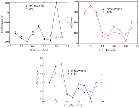
Figure 3.1 represents the electronic properties of BiTe with 9 different Se concentrations at room temperature, with a comparison between SPS and MW sintered samples for each. The Seebeck coefficient of 0.1, 0.2, 0.3, and 0.7 showed improvement in the Seebeck coefficient after the microwave sintering, with 0.3 showing the most
improvement. 0.5, 0.6, and 0.9 didn’t show any change, and 0.4 and 0.8 showed a reduction in Seebeck with 0.8 switching to p-type properties. Except for 0.1 and 0.8, all samples showed improvement in electrical conductivity after MW sintering. Generally, an increase in Seebeck is due to a reduction in charge carrier concentration. But since samples with 0.2, 0.3, and 0.7 show improvement in Seebeck and electrical conductivity, it must be due to a
28
0.0 0.2 0.4 0.6 0.8 1.0
-300 -200 -100 0 100
SPS-MW-SPS SPS
0.0 0.2 0.4 0.6 0.8 1.0
SPS-MW-SPS SPS
0 100 200 300 400
0.0 0.2 0.4 0.6 0.8 1.0
SPS-MW-SPS SPS
0.0 0.2 0.4 0.6 0.8 1.0
Figure 3.1: Comparison of electronic properties of Bi2Te3-xSez samples at room temperature
for x=0.1 to 0.9 at room temperature. The dashed lines represent samples before MW sintering, and the solid lines represent samples after MW sintering. The x-axis represents the
29
40 80 120 160 200
1.0 1.5 2.0 2.5 3.0 0.2 0.3 0.4 0.5 0.6 0.7 0.8 0.9
40 80 120 160 200
0.0 0.2 0.4 0.6
0.8 0.2 0.3
0.4 0.5 0.6 0.7 0.8 0.9
Figure 3.2: On the left is the thermal conductivity data for all the samples after MW sintering. The sample with Se=0.6 has the lowest thermal conductivity, and the sample with
Se=0.2 has the highest thermal conductivity at room temperature. The figure on the right is zT for all the samples. The sample with Se=0.3 has the highest zT of 0.82 at around room
temperature.
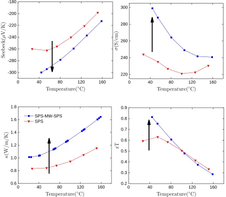
A comparative study for the samples with MW vs. SPS is shown in Figure 3.3. The microwave sintering results in significant improvement in the electronic properties of the material. Electronic conductivity and Seebeck coefficient generally have an inverse
30
0 40 80 120 160
-300 -280 -260 -240 -220 -200 -180
0 40 80 120 160
220 240 260 280 300
0 40 80 120 160
0.6 0.8 1.0 1.2 1.4 1.6 1.8 SPS-MW-SPS SPS
0 40 80 120 160
0.2 0.3 0.4 0.5 0.6 0.7 0.8 0.9
31 Table 3.1: Atomic composition of x= 0.3 and 0.8 before and after CMW sintering. It is observed that the post MW sample for Se0.3 has lost Te, which can be attributed to Te loss
during the process. The atomic percentage
Bi2Te2.7Se0.3 As-synthesized
Bi2Te2.7Se0.3 -MW450 processed
Bi2Te2.2Se0.8 As-synthesized
Bi2Te2.2Se0.8 -MW450 processed
Bi2Te2.2Se0.8 -MW500 processed Se 4.59 3.97 5.07 11.9 13.85 13.98 13.55 Te 54.53 54.65 37.82 45.77 44.82 45.58 44.1 Bi 40.88 41.38 57.11 42.33 41.33 40.44 42.35
EDS characterization was performed on x=0.3 and x=0.8 samples. The as-synthesized samples were close to stoichiometric composition. In the case of the x=0.3 composition the MW processed sample was away from the initial stoichiometry. It was depleted in Te. This might be due to the vaporization of the Te during the process. Due to the low vapor pressure of Te, it is possible for the release of Te atoms from the matrix. The Te depletion can result in extra electrons resulting in improvement in n-type properties. This wasn’t observed for the x=0.8 post MW sample. The improvements in zT were still observed for the same.
3.4Conclusion
32 is an exciting result, and further study is needed to optimize pulsed MW sintering for
33
Chapter 4:
Optimization of Bi
2Te
2.8Se
0.2Cu
xfor
Wearable Application with a Focus on
Reproducibility
4.1Introduction
Thermoelectric generators (TEGs) are sustainable, noiseless solid-state devices that can directly convert a temperature gradient into electricity with no moving parts
[74,75,76,77]. These devices can be designed for different temperature applications by using the optimal material for that temperature range [78,79,80]. The efficiency of these generators depends on the figure of merit zT= S2σT/κ where S is the Seebeck coefficient, σ is the electrical conductivity, κ is the thermal conductivity ant T shows absolute temperature [81,82]. In this regard, TEGs designed for the wearable application have great potential use in the battery-less operation of devices with continuous operation of various physiological and environmental sensors [83,84,85].
Thermoelectric (TE) materials based on the bismuth telluride alloys, particularly BixSb(2-x)Te3 for p-type and Bi2TexSe(3-x) for n-type, are well known for their efficient
performance at the room temperature [86]. Poudel et al. [87] were able to improve the zT of Bi0.5Sb1.5Te3 using ball milling and hot pressing and achieve a peak zT of 1.4 at 100°C.
However, n-type bismuth telluride alloys are restricted by the low number of valleys at the conduction band compared to the valance band edges, which results in a lower Seebeck coefficient compared to p-type Bi2Te3 [86]. Besides, the bipolar effect in n-type bismuth
34 (>100°C) [74]. For example, researchers have shown a peak zT of ~1.2 above 170 °C for n-type Bi2Te2.7Se0.3 [88] and Bi2Te2.3Se0.7 TE alloys [89].
Furthermore, researchers [90,91] showed a lack of reproducibility for the synthesized bismuth telluride TE samples, precisely due to the considerable variation of carrier
concentration. This can be attributed to the uncertainty in the formation of tellurium
vacancies during the milling process [90]. As shown in Figure 1, Bi2Te3 crystal consists of a
repeating chain of -Bi-Te2-Te2-Bi-Te1-. Due to the weak Te2-Te2 wan der Waals bond and the high vapor pressure of Te, the crystal is susceptible to Te vacancies, which can drastically impact the number of charge carriers.
Figure 4.1: Crystal structure of Bi2Te3 consisting of repeating chains of -Te-Bi-Te-Te-Bi-Te-.
The Te2 atom can be dislodged from its position resulting in a tellurium vacancy (VTe) and 2
free electrons.
Doping strategy with Cu and Ag has been regarded in different studies to enhance the TE properties and reproducibility of n-type Bi2Te3 alloys[90,91,92]. This is due to the
interstitial occupation of these dopants, resulting in the stronger bonds between the layers of Bi2Te3 [93]. Even though this has been successful, the work still lacks depth in the different
doping concentrations tested. Also, the peak zT for these works is at temperatures higher than 100°C, which is not suitable for the wearable application, used in body heat harvesting TEGs (~ 30°C). In this work, the effects of Cu doping are studied on Bi2Te2.8Se0.2 alloy. The
35 optimum doping concentration, for the wearable TE application, is determined and analyzed with the corresponding improving mechanism.
4.2Materials and Methods
Bi2Te2.8Se0.2Cux was prepared using elemental chunks of bismuth (needles, 99.99%),
36 4.3Results and discussion
Figure 4.2 shows the Seebeck coefficients and electrical conductivities of multiple synthesized Bi2Te2.8Se0.3 samples. Even though the samples were prepared with powder of
the same stoichiometry, the thermoelectric properties of these samples varied significantly. Similar variations were observed by Liu et al. [90] in their study of Bi2Te2.8Se0.3 TE alloy.
They attributed this to the highly sensitive nature of Te vacancies and its relation to the defect formation. A single Te vacancy generates 2 free electrons [94], and even a small fluctuation in these defects can result in a significant variation of electronic properties of the material. The defect formation is sensitive to milling conditions and hot-pressing conditions [90]. Consequently, in the mentioned study [90], the repeatability of the Bi2Te2.8Se0.3 TE
alloy was enhanced and got an optimum zT equals 1.06 at room temperature.
40 80 120 160 200 240
-240 -200 -160 -120
Bi2Te2.7Se0.3 BM-SPS
40 80 120 160 200 240
200 400 600 800 1000
Figure 4.2: Electronic properties of 7 samples of Bi2Te2.7Se0.3 processed using ball milling
37 Figure 4.3 illustrates the electronic properties for various Cu doped Bi2Te2.7Se0.2
samples. The Seebeck and conductivity indicate that for 0% and 0.0125% Cu, the material behaves as an intrinsic semiconductor at room temperature. The Seebeck decreases rapidly with an increase in temperature, and the conductivity increases quickly as well. This can be attributed to the rise in thermal charge carriers with an increase in temperature [86]. For Cu concentration of 0.025 and more, the Seebeck value is pinned and follows the trend for a degenerately doped semiconductor [86]. For Cu concentrations of 0.05, the material is highly degenerate, which results in a low Seebeck and high electrical conductivity [86].
40 80 120 160 200 240
-280 -240 -200 -160 -120
Cu-0.05% Cu-0.025% Cu-0.01875% Cu-0.0125% Cu-0%
40 80 120 160 200 240
200 400 600 800 1000 1200 1400
Figure 4.3: Electronic properties of Bi2Te2.8Se0.2 doped with different copper concentrations.
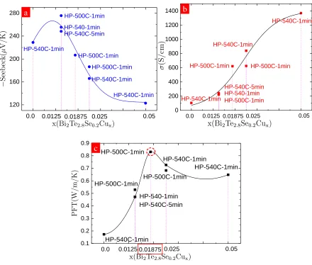
38 temperature with longer holding times. Using this knowledge, we found that the optimal recipe for our material is a Cu doping of x=0.01875 sintered at 500C for a soaking time of 1min.
y0 = 124.35596, xc = 0.08558 w = 0.22252, A = 39.64433 sigma = 0.11126, FWHM = 0.262
Height = 142.15223
HP-540C-1min HP-540-1min HP-540C-5min HP-500C-1min HP-500C-1min HP-540C-1min HP-500C-1min HP-540C-1min 0.05 0.025 0.01875 0.0125 0.0 120 160 200 240 280 HP-540C-1min HP-540-1min HP-540C-5min HP-500C-1min HP-500C-1min HP-540C-1min HP-500C-1min HP-540C-1min 0.05 0.025 0.01875 0.0125 0.0 0 200 400 600 800 1000 1200 1400
A1 = 12.45511, A2 = 1407.94849 LOGx0 = 0.23873, p = 5.6671 span = 1395.49338, EC20 = 1.35671
EC50 = 1.73271, EC80 = 2.21291
HP-540C-1min HP-540-1min HP-540C-5min HP-500C-1min HP-500C-1min HP-540C-1min HP-500C-1min HP-540C-1min 0.1 0.2 0.3 0.4 0.5 0.6 0.7 0.8 0.9 0.05 0.025 0.01875 0.0125 0.0
Figure 4.4: Room temperature data for different Cu doping and SPS temperature and their effects on a) Seebeck, b) electrical conductivity, and c) power factor of Bi2Te2.8Se0.2. The
peak power factor is for a copper concentration of 0.01875.
After the initial study on the optimal doping levels, the reproducibility of the material properties was evaluated. Bi2Te2.8Se0.2Cu0.01875 alloy was used since it showed the highest
power factor compared to other concentrations of Cu dopants. Three ingots of 10 grams each were prepared, and then 3 samples were sintered from each ingot. The resulting samples were
a b
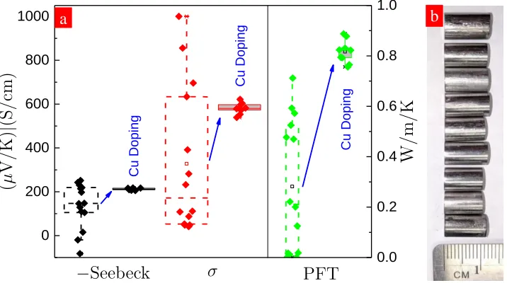
39 characterized, and the room temperature electronic properties were analyzed, as shown in Figure 4.5. The TE characteristics of Cu doped samples showed significant improvement in reproducibility compared to undoped samples. Furthermore, samples made from different ingots also showed similar properties. Since the only difference in the two sets of samples is the doping, the inclusion of Cu must be the cause of this improvement. Multiple studies [95,96,97] have shown that at lower concentrations, Cu atoms occupy interstitial positions in the lattice. Also known as intercalation, this results in the strengthening of the Te2-Te2 bond [90]. The result is a decrease in the fluctuation of Te vacancies (VTe) and, therefore, less
variance of charge carriers.
0 200 400 600 800 1000
Cu Dop
ing
Cu Dop
ing
Cu Dop
ing
0.0 0.2 0.4 0.6 0.8 1.0
Figure 4.5: a)Statistical data for all 9 ingots fabricated with a copper concentration of
0.01875. It is a significant improvement to undoped samples and shows a higher power factor compared to the undoped sample. b) The 9 samples used for this reproducibility study.
40
40 80 120 160 200
0.8 1.0 1.2
40 80 120 160 200
0.4 0.6 0.8 1.0 1.2 1.4
Figure 4.6: a) Thermal conductivity, b) zT values of Bi2Te2.8Se0.2Cu0.01875 alloy (black line)
Finally, the samples were characterized for their thermal properties (Figure 6.a). The lowest thermal conductivity was measured at a temperature around room temperature as 0.75 (W/mK). Besides, the calculated zT values showed a peak of 1.2 at room temperature (Figure 4.6.b). It’s worth noticing that the average zT of 0.88 was determined for the 9 samples at room temperature. Bi2Te2.8Se0.2 is more suitable for room temperature application compared
to Bi2Te2.7Se0.3 [90]when doped with copper since the peak zT is at room temperature. More
than 60 samples, of Bi2Te2.8Se0.2 and Bi2Te2.7Se0.3, were fabricated for this optimization
study. The lower charge carrier levels of Bi2Te2.8Se0.2 were found to be ideal for optimizing
the power factor to room temperature using copper doping. Compared to other studies, on n-type Bi2Te3, these are the best reported values for wearable applications.
41 Table 4.1: Comparison of room temperature properties of this study and other studies on
n-type Bi2Te3.
Composition κRT(W/m/K) zTRT Ref.
1 Bi2Te2.7Se0.3 1.15 0.9 [98]
2 Bi2Te2.79Se0.21 1.0 1.1 [99]
3 Bi2Te2.3Se0.7 1.2 0.85 [89]
4 Cu0.01Bi2Te2.7Se0.3 1.1 0.9 [90]
5 Bi2Te2.7Se0.3 0.9 0.8 [100]
6 Bi2Te2.7Se0.3 0.7 0.7 [88]
7 Bi2(TeSe)3 1.3 0.75 [101]
8 Bi2Te2.4Se0.6 1.5 0.9 [102]
9 Bi2Te2.7Se0.3 2.0 0.8 [103]
10 Cu0.05Bi2Te2.85Se0.15 1.2 0.8 [104]
11 Cu0.01875Bi2Te2.8Se0.2 0.75 1.2 This Work
To compare the properties of the nanocomposite materials and commercial materials, we prepared two thermoelectric generators. Figure 4.7 shows the experiment setup and an image of the fabricated TEG. One with nanocomposite n-type, using the materials
synthesized in this study, and p-type and the other with COTS materials. The TEGs were 1cm2 with 48 legs of 0.6mm x 0.6mm cross-section, 3mm length, and a fill-factor of 20%. The fabrication and characterization will be discussed in greater detail in a forthcoming paper. Some initial characterization data is shown in Table 4.2 for the two TEGs. Both were placed on a hotplate at 33C. The nanocomposite TEG was able to maintain a higher
42 be boosted to power circuits, they must be interfaced with boost converters. The efficiency of a boost converter is directly proportional to the input voltage, so the higher voltage generated by the nanocomposite TEG results in better overall efficiency.
Table 4.2: Comparison of TEGs made with nanocomposite and commercial legs.
Figure 4.7: a) Characterization setup of the device. The hotplate is set to 33C to mimic skin temperature. b) Images of TEGs with 48 legs.
4.4Conclusion
Bi2Te2.8Se0.2 was investigated as an n-type material for wearable applications. The
thermoelectric properties were optimized for the room temperature application by testing Cu doping levels of 0.0125, 0.01875, 0.025, and 0.05. These doping values were screened based on the binary search method, and the optimal level of copper was found to be 0.01875%. The material showed excellent reproducibility, which was attributed to the Cu doping. Cu
intercalation resulted in reducing the VTe fluctuation and, therefore, repeatable properties.
Also, SPS conditions were shown to impact on the dopant activation with higher a
43 temperatures and holding times, which provides higher activation. Characterization of
44
Chapter 5:
Experimental Synthesis and
Thermoelectric Characterization of Bi-Te-S
Compound
5.1Introduction
Since two-third of the energy in the world is wasted as heat, there is an economic and environmental benefit to recover this low-grade energy into the appropriate energy form such as electricity [105,106]. Thermoelectric (TE) compounds via interchanging the thermal energy into electricity open the opportunities to generate environmentally friendly energy. However, the required action must be taken to improve the efficiencies of the current TE products. Based on the dimensionless figure of merit, which assesses the performance of the TE material, several parameters and phenomena can modify the TE features [107,108].
In this field, several strategies have been employed in improving the TE factors, for example, nanostructuring to modify the Seebeck coefficient via the energy filtering or decreasing the thermal conductivities by providing more grain boundaries and phonon scattering [109, 110]. Also, the corresponding factors of the electrical conductivity can be modified via the manipulating the microstructure.
𝜎(𝐸) ≅ 𝑒2𝜏(𝐸)𝑉
𝑥2(𝐸)𝑛(𝐸) (−
𝜕𝑓𝑒𝑞
𝜕𝐸 ) (2)
𝜏(𝐸): nonequilibrium transport in the heterostructures
n(E): carrier pocket engineering
45 In this respect, modulation, via mixing two phases and making a mixed phase, has been studied to enhance the thermoelectric properties [111]. In this study, a new thermoelectric alloy was prepared and investigated by mixing two compounds of Bi2Te3 and Bi2S3.
Figure 5.1: Phase diagram of Bi-Te-S alloy [112]. 5.2Materials and method
Bismuth shots (Bi, 99.99%), tellurium chunks (Te, 99.99%), iodine chunks (I, 99.999%), and bismuth sulfide powders (Bi2S3, 99.99%) were weighed in the desired stoichiometry
46 inner diameter of 6mm and sintered in a custom hotpress in an argon environment. The samples were sintered at 540C for 5mins under a pressure of 220psi. This resulted in a rod of 6mm diameter and 12-14mm length with a density of 97-99% of the theoretical value. The rod was used directly for 4 point probe measurement to get electric conductivity and Seebeck coefficient using a Linseis Seebeck-3 tool. A disc of thickness 700um was cut using a CNC wire saw, from these samples for thermal diffusivity measurement using a Linseis LFA system. Thermal analyses were performed in the same direction as the electronic property measurement. A Rigaku benchtop (miniguidance600) was used for the XRD measurement of samples and powders during the optimization process.
5.3Results and discussion
X-ray diffraction (XRD) analysis of the five different compositions is shown in Figure 5.2. These compositions consist of different ratios of Bi2Te3-Bi2Te2S phases. The peak
47
20 40 60 80
Bi2Te2S1
Bi2Te3 Bi2Te2.75S0.25 Bi2Te2.5S0.5 Bi2Te2.25S0.75 Bi2Te2S1
Bi2Te3
Figure 5.2: XRD analysis of the 5 different compositions of the Bi-Te-S system showing two separate phases Bi2Te3 and Bi2Te2S1.
Figure 5.3 shows the thermoelectric properties of the different Bi-Te-S compositions. These compositions were directly measured from the ingot without any form of ball milling. Samples show a negative Seebeck coefficient, which shows that the samples were all n-type. A comparison of the sample with S=0 and S=0.25 shows that they are both extrinsic
48 Based on Bergman's theory[113], the zT of a composite material cannot be higher than the individual constituents. However, we show here that it is possible to make a material with greater zT compared to their parts. This is confirmed by the sample with S=0.25, which shows a much higher zT of 0.7 compared to its components. This indicates some form of nanostructure consisting of the two phases resulting in non-equilibrium transport. This is an exciting result and could be applied to other combinations of high conductivity-high Seebeck materials that don’t form an isomorphous solution.
40 80 120 160 200 240
0 200 400 600 800 1000
Bi2Te3
Bi2Te2.75S0.25
Bi2Te2.5S0.5
Bi2Te2.25S0.75
Bi2Te2S1
40 80 120 160 200 240
-220 -200 -180 -160 -140 -120 -100
40 80 120 160 200 240
0.0 0.2 0.4 0.6 0.8
0 50 100 150 200 250
0.6 0.8 1.0 1.2 1.4 1.6
49 The next study was focused on improving thermoelectric properties of the intrinsic composition with S=0.5, and the results are plotted in Figure 5.4. There were two
modifications to the original recipe- nanostructuring using ball milling to reduce thermal conductivity and Iodine doping to improve the power factor of the material. When comparing the thermal conductivity before and after ball milling, it remains the same. This indicates that there are already nanostructuring due to the quenching steps performed on the
nanocomposite. The nanostructure was frozen during this step, resulting in low phononic thermal conductivity. Doping of this material with iodine resulted in significant
50
40 80 120 160 200 240
0 200 400 600 800 1000 1200
1400 Bi2Te2.5S0.5
Bi2Te2.5S0.5-I0.005
Bi2Te2.5S0.5-I0.01
Bi2Te2.85S0.15
Bi2Te2.85S0.15-I0.005
Bi2Te2.85S0.15-I0.01
40 80 120 160 200 240
-250 -200 -150 -100 -50
40 80 120 160 200
0.0 0.1 0.2 0.3 0.4 0.5 0.6 0.7 0.8
0 50 100 150 200
0.6 0.8 1.0 1.2 1.4 1.6 1.8 2.0
Figure 5.4: Thermoelectric properties of samples with S=0.5 and 0.15 with different Iodine doping levels.
51 This value is also higher than its individual constituents, which confirms that it is possible to make materials with better efficiency than its constituents.
5.4Conclusions
The effects of sulfur dopants on the Bi2Te3 alloy were investigated. The sulfur element
52
Chapter 6:
Thermoelectric Generator Device
Fabrication
6.1Introduction
Material optimization is vital to achieving higher efficiency generators. However, material research alone isn’t enough for making peak energy conversion. Other factors, such as contact resistance, can play a significant role in the overall performance of a system. Since TEGs are electrically in series, bad contact resistance can add up and reduce the power output of a device. Body heat harvesting for wearable applications has additional challenges that require the optimization of material and devices collectively. Modeling done by
Francisco et al. [114] has shown that due to skin resistance and air resistance, the temperature difference across the thermoelectric material is only a few degrees. This limitation must be considered when designing leg geometries. Also, the emphasis on reducing thermal
conductivity is more significant than just increasing zT since the device is limited by the parasitic thermal resistances.
53 the small temperature difference implies that high aspect ratio legs are needed for wearable applications.
This chapter covers in detail a process for metalizing and dicing high aspect ratio legs from synthesized materials. The process is designed such that the legs geometry can be modified depending on the need of the use. Device fabrication steps are also discussed in detail followed by some characterization results of modular devices made by nano-composite materials.
6.2Design and Methodology
6.2.1 TEG Design
The TEG design parameters are listed in Table 6.1. The headers were custom
designed using SolidWorks and were manufactured by D. K. Thermals. They were designed to be modular to have the flexibility to connect as many in series depending on the power requirement. The material of the header was chosen to be an aluminum nitride, which, compared to alumina, has 10x higher thermal conductivity. This should improve heat rejection of the device compared to commercially available headers.
Table 6.1: Design parameters for a single TEG.
Parameter Value
Area 10mm x 10mm
Header thickness 0.25mm
Header material Aluminum Nitride Fill Factor 20%
No. of Legs 48 Leg length 3mm
54 The electric pad layout of the top and bottom header is illustrated in Figure 6.1 along with a scaled exploded view of a TEG device. Once soldered, the top and bottom headers form a series electric circuit of the n and p legs.
Figure 6.1: Top and bottom header with metal pads along with a scaled drawing of a device.
6.2.2 Sample preparation
55 extrinsic semiconductors. zT shows a rising trend with decreasing temperature. The thermal conductivity is lowest at room temperature. The nine samples prepared for this study are outlined in Figure 6.4.
300 400 500 0.6 0.8 1.0 1.2 1.4
Figure 6.2: Statistical data for the final 9 p-type samples used for device preparation.
0 50 100 150 200 250
0.2 0.4 0.6 0.8 1.0 1.2 0.8 1.0 1.2 1.4 1.6 1.8
0 50 100 150 200 250
240 260 280 300 320 340 360 380 140 160 180 200 220 240 260 280 300
56 Figure 6.4: The 9 p-type samples used for preparing devices.
6.2.3 Dicing, Surface preparation, and Metallization
Samples of length 13-14 mm, similar to ones in Figure 6.4, were consolidated for both n-type and p-type legs. These samples were then diced to 3 mm thick discs using a CNC wire saw. This thickness is going to be the final thickness of the legs and can be adjusted for the required dimensions. Different feed speeds and wire speeds were tested for optimum surface roughness. Faster feed speeds resulted in a highly rough surface but left deep
trenches. Slower speeds did not leave deep trenches but required further surface preparation. Without any surface preparation, diced discs showed poor adhesion to deposited metal. After the wire saw processing, the discs were cleaned with a sequence of 5-minute sonication in methanol, acetone, and isopropyl alcohol.
Figure 6.5: N and P-type discs after dicing and cleaning.
57 flaking. This could be attributed to under etching of the Bi-Te surface resulting in weak structures.
Interestingly, the same etching did not work for the p-type material. Different recipes of the bromine acid were used, but instead of increasing roughness, they became smooth. This could be due to the different composition of p-type material, which has a smaller amount of Bi2Te3. Thus, the p-type discs were treated using an 800-grit sandpaper polish.
Electroplating was initially used to metalize with copper, tin, and gold. Copper plating showed promise; however, it lacked good adhesion and uniformity. Furthermore, since more than 50 discs had to be metalized on both sides, electroplating was not a scalable option. Due to this, and amplified uniformity issues with larger batches of samples, alternative large area methods were explored. The second method considered was an e-beam deposition. This method improved on the scalability because an approximately 6” wafer area could be
uniformly coated. Test wafers were deposited with copper using an e-beam system. This also was not the ideal method to metalize the samples. Firstly, the rate of deposition was
prolonged, and the system would not be able to deposit >100nm necessary for proper contacts. Secondly, the adhesion of the deposited metal was inferior and would easily peel off following leg dicing steps. Finally, since the system could only deposit copper, it would require further metallization steps to deposit an inert metal with excellent adhesion to the solder, which added additional surface cleaning steps to the process.
The third method tested for metal deposition was DC sputtering. This is a standard method used by industry and has advantages such as faster deposition rates and
58 preparation using bromine acid chemical etch, and sandpaper physical etch. One of the tests is illustrated in Figure 6.6.
Figure 6.6: 6 n-type (top) and 6 p-type (bottom) samples loaded on a 4" silicon wafer using double-sided Kapton tape. The physical etch numbers represent sandpaper grit size.
Based on these tests, the optimal recipe was 2 min wet etch for n-type and an 800-grit polish for p-type material. Devices made from this recipe, however, displayed device
59 Figure 6.7: IR images of the top of the device. Hot spots indicate poor contact resistance.
![Figure 1.2: The Seebeck coefficient, which is +ve for p-type and -ve for n-type materials as a function of initial Te concentration [13]](https://thumb-us.123doks.com/thumbv2/123dok_us/1759775.1226164/19.612.146.490.72.325/figure-seebeck-coefficient-type-materials-function-initial-concentration.webp)