Gregory T. Brauns
Center for Communications and Signal Processing Electrical and Computer Engineering Department
North Carolina State University
BRAUNS, GREGORY T. ZSIM: A Table-Based Z-Domain Simulator For
Delta-Sigma Modulators (Under the direction of Dr. John J. Paulos, Dr. Michael B. Steer, and Dr. SasanH. Ardalan.)
Delta-sigma modulation is one of a class of systems which use oversampling
and L-bit quantization to achieve high resolution AID conversion at a lower rate. However, their implementation and wide-spread use is limited by the inadequacy of analytic and simulation tools. A peculiarity of the delta-sigma modulator is
that it contains a mix of continuous analog and sampled digital signals, as well as
strong nonlinearities, and requires thousands of simulation cycles for performance
evaluation.
The purpose of this work was to obtain a fast and accurate simulator for
delta-sigma modulators. Speed is achieved by modeling the circuit in block
diagram form and accuracy is achieved by the use of table models developed from
SPICE or CAzM device-level simulations. The use of table-based methods allows for simulation of nonidealities with increased speed over conventional device-level
simulators. Post-processing routines are included in ZSIM to perform digital signal processing for performance evaluation. The table-based simulator, which uses
linear interpolation routines, has been tested on idealized circuits represented by
difference equations and a second-order switched-capacitor circuit represented by
SPICE and CAzM table models. Results show that system performance is
IJIST OF TABLES v
LIST OF FIGURES VI
Chapter 1:DELTA-SIGMA MODULATION
u
u
oo...
1 Chapter 2: INTRODUCTION TO TABLE-BASED SIMULATION0..0...
6201 Motivation 0... 6
2.2 CAD Concept for Sampled Data Systems 0 I I 8
2.3 Development of an Efficient Simulator 11
Chapter 3: ZSIM: A NONLINEAR Z-DOMAIN SIMULATOR 15
3.1 Program Structure
0...
153.2 Input Features 19
3.2.1 Control Commands 19
3.2.2 Circuit Descriptions 21
3.2.3 Filtering Analysis 22
3.3 Tables Cl ••.O...•• O... 24
3.3.1 Set-up and Generation
0.00 •••••.••.••••••.••••••••••••••••• 0...
243.3.2 Interpolation 26
3.4 Output Features 28
3.5 Memory Requirement 33
3.5.1 TableStorage 33
3.5.2 Integrator Storage, Example of Modularity... 34
3.6 Computational Speed 37
Chapter 4: BENCHMARK SIMULATIONS 40
4.1 High-level Benchmark: Ideal Table vs. Difference Equation 41
4.1.1 Voice Band Circuit 41
4.1.2 Simulation Results 42
4.1.2.1 Baseband Spectrum 47
4.1.2.2 Signal-to-Distortion Ratio 90. 49
4.1.2.3 Interpolation Accuracy 52
4.2 Low-Level Benchmark: Device-Level vs. Difference Equation 53
4.2.1 ISDN Circuit 53
4.2.2 Table Generation .. 55
4.2.3 System Performance 65
Chapter 5: FUTUREINVESTIGATIONS 69
5.1 Tables and Interpolation 69
5.2 ZSIM Additions ~... 71
LIST OF REFERENCES 73
APPENDICES 76
A: ZSIM User'sManual 76
B: SPICESimulation Example 102
LIST OF TABLES
Table 3.1: Summary of control commands 20
Table 3.2: Run time comparison using tables, difference equations, and SPICE 38 Table 4.1: SDR summary for ideal table and difference equation simulations o o o o u o . " 49 Table 4.2: Summary of integrator simulation for cycle #249 ..0 0 0 . . 0 0 0 0 0 . . 52 Table 4.3: SDR summary for ideal table, SPICE table, and CAzM table
LIST OF FIGURES
Figure 1.1: Block diagram of a first-order delta-sigma modulator .. Figure 1.2: Sample set of signals for a first-order delta-sigma modulator . Figure 1.3: Block diagram of a first-order delta-sigma demodulator .. Figure 2.1: Flowchart of a CAD tool for delta-sigma modulators . Figure 2.2: Second-order delta-sigma modulator .. Figure 2.3: Second-order delta-sigma modulator with fictitious sample-and-holds
...
Figure 2.4: Second-order z-domain delta-sigma modulator ..
Figure 3.1: Simulation flowchart for ZSIM .
Figure 3.2: Details of the Table Generator Module .
Figure 3.3: Post-Processor Module flowchart .
Figure 3.4: A ZSIM integrator .
Figure 3.5: Format of a table for N=3 and M=2 ..
Figure 3.6: A planar view of table grid with interpolation points .. Figure 3.7: A sample collection of bins around the signal . Figure 4.1: Ideal delta-sigma modulator system for CODEC application ..
Figure 4.2: CODEC integrator
#1
ideal table .Figure 4.3: CODEC integrator #2 ideal table .
Figure 4.4: Graph representation of integrator
#1
.
Figure 4.5: Graph representation of integrator #2 . Figure 4.6: CODEC baseband spectrum for input= -
15 dB .. Figure 4.7: CODEC baseband spectrum for input = 0 dB .. Figure 4.8: SDR versus input amplitude for CODEC delta-sigma modulator .. Figure 4.9: SDR differences (difference equation - table) versus input amplitude...
Figure 4.10: Second-order delta-sigma switched-capacitor circuit .
Figure 4.11: ISDN integrator
#1
ideal table .Figure 4.12: ISDN integrator #2 ideal table .
Figure 4.13: ISDN integrator #1 table generated from SPICE .. Figure 4.14: ISDN integrator
#1
table generated from CAzM ..Figure 4.15: ISDN integrator #2 table generated from SPICE . Figure 4.16: ISDN integrator#2 table generated from CAzM . Figure 4.17: Circuit errors exhibited by SPICE and CAzM tables . Figure 4.18: SDR versus input amplitude for ISDN delta-sigma modulator . Figure 4.19: ISDN baseband spectrum for input
= -
10 dB .CHAPTER
1
10
DELTA-SIGMA MODULATION
Delta-sigma modulation [1,2] is one of a class of systems which use oversarn-pIing and I-bit quantization to achieve high-resolution AID conversion at a lower rate. Oversampling is attractive in that precise analog anti-alias filtering can be omitted. Instead, digital FIR lowpass filters, which are relatively insensitive to coefficient roundoff, are used after the modulator to perform decimation and anti-alias filtering. Decimation is required to achieve conventional Pulse Code Modula-tion (PCM) signals by reducing the sampling rate of the l-bit data stream gen-erated by the modulator. Another attraction is that delta-sigma modulators can be implemented with few precision circuits and precise component tolerances are not needed [3,4,5,6]. Delta-sigma modulators can be easily implemented in digital MOS IC technologies [3] through the use of switched-capacitor circuits. This approach has recently gained increased attention [3,7,8,9]. Digital MOS technol-ogy also lends itself to the implementation of complex decimating digital filters.
demodula-xft)
p(t)
Figure 1.1: Block diagram of a first-order delta-sigma modulator
tor. An example set of these signals is presented In Figure 1.2. The feedback works to minimize the error signal, e(t), given by
e(t)
=J
[x(t) - p(t)]dt.
(1.1)The error signal is quantized by a comparator which samples and holds the binary
code for one clock cycle in an attempt to track z
(t)
with p(t). Therefore, theout-put is driven so as to match the signal directly, at least in an integrated error
sense. The maximum encodable input signal is equal to the amplitude of the
out-put pulses [2]. Therefore, overloading of the system is independent of the signal
frequency and the system has no significant problems in tracking the signal.
One advantage of delta-sigma modulation is that the corresponding
demodu-lator is simple and does not require analog circuitry, as shown in Figure 1.3.
(a)
x(t)
(b)
z(t) -
P(t)
(c)
~(t)(d)
p(t)
I I I I I
-
-~~ ~
,.. ~
... ~
..
,......
....
- -
-
-
..
.-
..
--..
...
-...
...II ... ...
--
..
--
1 I I I IFigure 1.3: Block diagram of a delta-sigma demodulator
them through a lowpass filter. The lowpass filter reduces the effects of
quantiza-tion by removing the out-or-band noise and the signal images at multiples of the
clock frequency.
Although delta-sigma modulation is conceptually simple, the system is
difficult to analyze. The nature of the modulator's structure prohibits simple
analysis - the quantizer is a nonlinear device, the sample and hold function causes
the output pulses to be dependent on time and amplitude, and the feedback loop
introduces stability problems. Also, if a random input is applied to the system,
evaluation of the noise content in the output signal is difficult. Consequently, the
The following chapters will introduce and demonstrate a novel simulator for
delta-sigma modulators.
ZSIM
(a nonlinear Z-domain STh1ulator), uses table-basedmethods in a block-level configuration so that fast and accurate simulations can be
obtained. Chapter 2 discusses the need for a new circuit simulator of this type and
introduces the concept of table-based simulation for delta-sigma modulators.
Chapter 3 goes into the details of the program structure, describes the table data
structure, and presents computational speed comparisons of the table-based
simu-lator versus conventional device-level simulators. Some sample results are
presented in Chapter 4 which demonstrate the validity of the table method. Also
presented are simulated results of a complete circuit intended for use in ISDN.
CIfAPTER
2
2. INTRODUCTION TO· TABLE-BASED SIMULATION
2.1.
MOTIVATION
Delta-sigma modulators have been successfully used in voice-band CODECS
[6] and for the V-interface of an Integrated Services Digital Network (ISDN), where
monolithic high resolution AJD conversion is required for echo cancellation [5].
However, the implementation and wide-spread use of delta-sigma modulators is
partly limited by the inadequacy of analytic tools and simulation tools. A
pecu-liarity of the delta-sigma modulator is that it contains a mix of continuous analog
and sampled digital signals, as well as strong nonlinearities, which complicate the
development of analytic and numerical design aids.
Recent developments in analytic techniques for delta-sigma modulators
[10,11,12,13,14,15J have increased the understanding of the signal-to-distortion
ratio, quantization noise spectra and stability of these circuits. Unfortunately,
these techniques do not include circuit nonidealities. Only numerical simulations
can provide the required confidence in design, final optimization of system
perfor-mance, and investigation of novel circuit topologies. Until now numerical
eircuit-level simulators (e.g. SPICE [16]), and numerically efficient difference
equa-tion simulators, which cannot capture circuit phenomena
[17].
The speed ofsimu-lation is of overwhelming importance as the circuit must be simulated for a large
number of clock cycles, often tens of thousands. While being rapid, difference
equation simulations cannot easily include component effects such as slew-rate
lim-iting, noise, hysteresis, clock feed-through, and many types of nonlinearity
associ-ated with some types of comparators.
The problem of simulation speed has been solved in various ways. For
instance, utilizing a computer's full capabilities by writing machine dependent
code can improve simulation speed up to 20 times [18). Bypassing a simulation cycle, if little change occurs in the terminal voltages of a device, is another method of increasing simu.lation speed. Also, the addition of theoretical circuit predictions
aids in developing more efficient algorithms. Table look-up methods have also
been used recently in the speed-up of computer-aided analysis, especially in the area of MOSFET modeling [19,20,21]
Table look-up methods offer several advantages over other analytical and
numerical methods. Tables allow nonlinear as well as linear system equations to be
modeled and solved. Also, computation time is saved for every simulation once a
table is created and stored in memory. Tables allow for the re-use of data rather
than solving the same system of equations over and over for each time point or for
Table look-up methods are also economically practical. Todny's low cost
memory units allow for storage of virtually any number of tables of almost any
size. Even if secondary storage devices are used rather than the computer
semicon-ductor memory, the milliseconds of access time are still competitive with the
minutes of CPU time needed for other simulation methods.
The advantages of speed and accuracy with table-based simulation has
appealed to many researchers
[22].
Tables are being used for MOSFETs intransistor-level circuit simulation [19,20,21,23,24,25,26, 27J where more than half
of the total simulation time is often required for evaluation of the MOSFET
models. Microwave circuits are also being simulated with tables [28, 29]. The goal
of this work is to use tables to represent mixed-mode (analog and digital) feedback
sampled-data systems such as delta-sigma modulators.
2.2.
CAD CONCEPT FOR SAMPLED DATA SYSTEMS
The concept of integrating analytical tools, difference equation simulation and
table-based simulation, with appropriate postprocessing analysis is illustrated in
Figure 2.1. Using the analytical tools developed in [10,11,12,13,14], the pa~ame
ters of a candidate delta-sigma mod ulator are qu ickly derived for a given desired
system performance such as signal-to-noise or signal-to-distortion ratio. These
parameters include the oversarnpling ratio, the order of the modulator (first,
"
Analytical Tools
Difference Equation Simulation
Circuit-Level Simulation
...
...
Table GenerationTable-Based Difference
'-~~~I Equation Simulation
...
...
Post-Processing:Decimation and Baseband Filtering Signal to Distortion Calculation
Figure 2.1: Flowchart of a CAD tool for delta-sigma modulators
other parameters.
A13 an example, Ardalan and Paulos
[14]
have expressed the signal-to-noiseratio of a sinusoidally excited modulator as a function of input amplitude. In
addi-tion, the variance at various nodes in the circuit both for the signal component and
ampli-tude increases these variances rapidly increase leading to saturation in actual
cir-cuits. Analysis of these variances, in conjunction with algebraic expressions of the
specified performance requirements, can be used to determine the system
parame-ters of the modulator such as the oversampling ratio, the order of the modulator,
and the integrator gains. Using the expressions for the frequency response of the
decimation filters
[12],
it is then possible to compute the aliased noise in thebaseband and subsequent reduction in signal-to-noise-plus-distortion ratio
(S/(N+TlID)) for different weighting and tap lengths.
After the system parameters have been determined using the analytical tools,
difference equation simulations are combined with the actual decimation and
baseband filters to verify the performance of the modulator ignoring potential
cir-cuit limitations. At this stage, circir-cuit-level implementations are considered, and
tables are generated, using circuit-level simulators such as SPICE, for the
subsys-tems that make up the modulator. Tables are generated for the subsyssubsys-tems that
make up the modulator. Using these tables, ZSIM captures circuit-level
nonideali-ties but still achieves rapid simulation at the subsystem level.
During each stage of the design and simulation process the designer can
iterate between the simulation systems find ana lyt.ical tools to determine thp circuit
which is most appropriate in terms of complexity, technology, and other
2.3.
DEVELOPMENT OF AN EFFICIENT SIMULATOR
The simulation of delta-sigma circuits is complicated by oversampling and the
presence of both analog and digital signals. This results in time-domain
simula-tions being prohibitively time consuming. However, delta-sigma modulators are
sampled data systems, so it is possible to model the performance of individual
sub-systems of the modulator at the sampling intervals. Continuous-time information,
such as the circuit waveform between sampling intervals and the circuit state at
internal subsystem nodes, are not required for accurate system-level simulation.
Thus it is possible to use a z-domain description of the system. The utility of
difference equation simulators is that they operate in the linear z-domain and so
computations are kept to a minimum. Often, however, it is not possible to develop
sufficiently accurate difference equations for practical delta-sigma circuits because
of complex dependencies on nonlinearity, hysteresis, clock feed-through, slew-rate
limiting, and finite gain-bandwidth-product of the subsystems. ZSTh1, using table
methods, is a natural extension of difference equation simulation and enables these
effects to be modeled using a multi-dimensional table.
The development of ZSIM is analogous to that of the difference equation
method. A second-or.der delta-sigma modulator is shown in Figure 2.2. With the
addition of fictitious sample-and-holds, as in Figure 2.3, a delta-sigma modulator
can be represented in the z-domain as in Figure 2.4. This representation enables
the subsystems to be considered individually (although the input and output
imple-x(t)
Figure 2.2: Second-order delta-sigma modulator
p(t)
mentations of delta-sigma modulators use sampled data circuits and/or switched
capacitor circuits, the addition of fictitious sample and holds, if placed
appropri-ately, has no affect on circuit performance.
Consider the first integrator block of Figure 2.4. The output of this
subsys-tern can be linearly modeled by the product of its input and its transfer function,
as given by
y[z]
=
(XlHl[z] (x[z] - p[z])
where y
[k
1
is the integrator output and the transfer function is given by(2.1)
(2.2)
Since computer simulation uses discrete time steps, the function occurs in the form
of sequences. Converting the combination of Equation 2.1 and Equation 2.2 to a
x(t)
.:»:
f
s"r
p(t)-~
Figure 2.3: Second-order delta-sigma modulator with fictitious sample-and-holds
x[k]
Figure 2.4: Second-order z-domain delta-sigma modulator
Ie
y[k]
=
ellL
(x[n] - p[n])
n=-x
p[k]
(2.3)
k-l
y[k]
=
(XlL
(x[n] - p[n))+
Ql (x[k] - p[k))n=-oo
or
y[k]
=
y[k-I]
+
al (x[k] -p[k])
(2.5)Equation 2.5 represents the difference equation implementation of a simple
integra-tor used in most simulaintegra-tors. The limitation is that this function is linear. Physical
circuits may contain gain errors, saturation of the output, and comparator voltage
mismatches, which have no a linear relationship with the output. More generally,
x[k], y[k-I],
andp[k]
are independent variables foryrk]
with an unknownnon-linear relationship which can be described by
y[k]
=
T
(x[k], y[k-I], p[k])
(2.6)where
T
is a table look-up function. Subsystems in Z8IM are described byCHAPTER 3
3. ZSIM: A NONLINEAR Z-DOMAIN SIMULATOR
ZSIM is a nonlinear Z-domain SIMulator designed for simulation of sampled
data systems. ZSIM integrates analytic tools, a difference equation simulator, a
novel table-based nonlinear z-domain simulator, and digital signal postprocessing
into a workstation environment. The primary goal of ZSIM is development of an
accurate and fast simulator for delta-sigma modulators.
ZSIM has a user-friendly input format but lacks a totally stand alone topology
specification. Up to third order DSM's can be simulated using difference equations,
and first and second order DSM's can be simulated using table methods. Program
code is written in ANSI standard FORTRAN 77 and operation has been verified
on a DEC MICROVAX running either the Ultrix 1.2 or MICROVMS operating
system.
3.1. PROGRAM STRUCTURE
ZSIM is a completely modular program consisting of four major subdivisions
-an Input Module, a Table Generator Module, a Simulator Module, -and a
Post-Processor Module.
A
high level flowchart of the program is shown in Figure 3.1.cir-I
Input
--
- Table SimulatorPo~t-Generator
-
PrOCe!80rFigure 3.1: Simulation flowchart for ZSIM
cuit parameters) or variations of external parameters (such as clock rate or input
signal) in one computational run, as might be needed for a comparative analysis.
The Input Module's high level input capability allows for input to be taken
from the keyboard and/or from a disk file. Standard English commands are used
to diminish the need for a specific program environment language.
The Table Generator Module develops the tables that describe the
input-output characteristics of each subsystem. The functionality of the Table
Genera-tor Module is depicted in Figure 3.2. Basically, a decision is made whether to use a
difference equation representation of the circuit or a table representation of the
r---,
I create I
- -1
circuit-levelI table i
L- --J
create ideal table
y
N
read table or create difference
equation
Figure 3.2: Details of the Table Generator Module
presently a manual chore which has not as yet been automated. Automatic table
generation would involve running a circuit-level simulator, such as SPICE, for one clock cycle, extracting pertinent data, storing the data in a specific memory
loca-tion, and repeating the process until each position of the table contains simulated
data.
The Simulator Module performs simulations of the sampled data circuit using
table descriptions of individual subsystems or using difference equations for rapid
circuit investigations. Since topology specifications are currently ignored (except
order of the system. The topology is therefore fixed according to the order of the
modulator. The order of simulation for each subsystem at each clock cycle is as
follows: the input signal generator, the integrators in the order of signal
propaga-tion, and the comparator. The voltages at the input and output nodes of each
sub-system are stored in memory for processing during the next clock cycle.
The Post-Processor Module implements decimation and baseband filtering
and calculates system performance characteristics (in the frequency domain) in a
high-level fashion depicted in Figure 3.3. Flexibility is provided in that any
ele-ment of this module can be bypassed. For instance, an FFT may be performed on
the modulator bitstream before decimation occurs or baseband filtering may be
excluded completely. It is even possible to use parallel structures of these
ele-ments. For example, two different filters may be defined to operate on the output
of the decimator, with a different FFT analysis specified for each filter.
Baseband FFT,
Decimation
-
--
SystemFiltering
-Performance
A source file flowchart of the program can be found in the l.JSPT'R Manual
(Appendix A), with each routine separated into its corresponding module (Input,
Table Generator, Simulator, and Post-Processor). Note that all modules stem
from the file ZC~; ZC~ handles all commands in a modular fashion.
Addi-tional source code can be integrated into ZSIM by simply adding a command
recognition statement in ZCMD. Adding a new pre-processing or post-processing
subsystem, such as a digital filter, would be just one example of a modular
addi-tion. If a new subsystem, such as a multiplier, is desired for inclusion in the
Simu-lator Module, modification of the simulation command routine ZANA is also
required to add a new fixed topology option. The ZSIM source code is published in
[30], which may aid in the module addition process.
3.2.
INPUT FEATURES
3.2.1. Control Commands
Program organization and execution is controlled through the Input Module.
Two types of control commands exist: disk file input/output commands and circuit
control commands. The control commands are summarized in Table 3.1. Disk file
input/output commands are necessary to handle differences in interactive and
file-read executions of ZSIM. Flexibility is enhanced in that program overhead may be
included in the output, if so desired, with commands like ECHO ON, TITLE,
Table 3.1: Summary of control commands
Disk file
input/output Description
read open file for input
write open file for output
echo on/off echo input lines
eor close input data file
end temporarily close input data file title write line to output file
prompt write line to terminal
stop end ZSIM session
Circuit control Description
circuit define order of circuit
environment define external circuit parameters
init initialize quan tities
clear set all parameters to default
noise define Gaussian white noise at circuit nodes
dump store node values in a file
circuit and simulation parameters or specifications (CmCUIT, ENVIRONMENT,
INIT).
ENVIRON?v1ENT sets parameters such as sampling frequency and thenumber of clock cycles to execute. CLEAR is a user-friendly command which
resets all circuit parameters and subsystem definitions to default so that more than
one circuit can be simulated during one ZSIM session. NOISE is a Gaussian white
noise generator available to test system response for noise present at various circuit
nodes. Use of the generator has not been completely tested with respect to peak
noise values, i.e., the noise probability density function is not scaled to fit variable
may hr FFT bins or a time sequonreof voltages,
3.2.2. Circuit Descriptions
Delta-sigma modulator systems are defined by an input generator (GEN), an
integrator (SCINT), and a quantizer (QUANT). These subsystems are configured
to form the block delta-sigma modulator structure as previously depicted in Figure
2.4. With each subsystem definition, node numbers must be specified (although
circuit topology is hardwired) for memory allocation purposes.
Input signal types currently available include de, ramp, sinewave, and step
function. It is up to the user to insure that input signals do not exceed the circuit
power supplies. All parameters, such as amplitude, frequency, phase, delay, and
de
offset, are variables set by theGEN
definition statement.Since MOS Ie technology is generally used for delta-sigma modulators
[17],
the most common topology for the integrators will be a switched-capacitor integra-tor. Therefore, the switched-capacitor integrator (SCINT) command is used for ZSIM's integrator. For the purposes of simulation, the output of a SCINT is afunction of its inputs and its previous output and is described by a table. Each
SCINT command should be followed by a TABLE command when table
simula-tion is required. A discussion of tables will be presented in secsimula-tion 3.3.
Presently, the quantizer (QUANT), or comparator, is simulated as an ideal
circuit, i.e., tables are not used to describe the input-output transfer function of a
binary and is coded as +1 or -1. An offset may be specified for the eornparators
switching threshold.
Before a time consuming table generation is performed for a switch-capacitor
integrator, a difference equation model can be used. Simulation of the circuit with
this model can be used to validate the choice of integrator gains. To define a
difference equation model for the integrators, one EQUATION command replaces all SCINT , TABLE, and QUANT commands. Circuit topology is hardwired in equation mode; nodes are internally assigned numbers depending on the order of
the system. Parameters of the model include output saturation voltage, gain,
switched reference voltage, and finite-gain-bandwidth. See the User's Manual in
Appendix A for command usage.
3.2.3. Filtering Analysis
Filtering of the modulator output is included since in most applications the
oversampled data must be decimated to a workable frequency. Both FIR
decimat-ing filters and IIR baseband filters can be specified. FFT and other signal analysis
are available to measure SNR and SDR of the complete system, including
decima-tion and baseband filtering. The DECIMATE and SDR commands include the
specification of the circuit nodes which define a subsystem-like structure as
described earlier. This allows for flexibility of connections.
The DECIMATE command defines the type of FIR decimating filter and may
canonical tapped-delay line. Command inputs include a decimating factor
(INTDEC), the number of tapped delays (TAPS), and a windowing function
(WINDOW = uniform, triangular, or parabolic) which describes the tap weighting scheme. The weighting scheme is congruent to the impulse response of the filter.
Also, the decimation is performed by saving one sample out of every INTDEC
samples. The IIR baseband filter inputs include a decimating factor
(BBANDDEC), a special filter file (FILE), and the type of filter (TYPE
=
none,direct form, normalized lattice form, or cascade form). The special filter file is a
file that contains
1m
filter coefficients. Currently, these coefficients must begen-erated by the user through a separate routine that designs these IIR filters and
pro-duces the coefficient file (this routine is available from
ccsr-';
Version ZSIM:Oalincludes a file, VB.CAS, which specifies a cascade filter designed for decimation to
voiceband. VB.CAS has a 3.4 kHz rolloff for an 8 kHz sampling frequency.
The SDR command defines the digital signal post-processing. An SDR calcu-lation, which is based on the fast Fourier transform (FFT), may be performed on
any sequence of data as long as the number of bins in the sequence is a power of 2.
This criterion is necessary for the FFT simulation. Thus, an FFT may be
calcu-lated for the modulator bitstream or the decimated and filtered output. If
decima-tion is performed, the parameters in SDR must agree with those of DECllv1ATE.
This allows the SDR and DECIMATE routines to operate completely independent
of each other.
FOT an
son
calculation, the number of points (NFFT) needed fOT the FFTmust be specified. There is an NSKIP parameter that allows initial signal bins, which may represent transient circuit performance, to be ignored. Other
parame-ters are sampling frequency
(FS),
passband frequency(FB),
signal frequency(SIG-NAL), and FFT window type (FFTWINDOW = uniform, Hamming, or Blackman-Harris). Parameters that correspond to the decimation routine are the
number of FIR tapped delays (TAPS) and the decimation window (DECWIN-DOW). These two parameters are required to adjust signal frequencies and ampli-tudes which may be degraded by the filter. This problem is discussed later in the
"Output Features" section. Specifying DECWINDOW=ignore will let
SDR
assume that the filter has no degradation problems.
3.3.
TABLES
3.3.1. Set-up and Generation
The representation of circuit subsystems by tables allows discretization of
input/output data for linear and nonlinear regions of operation. Thus, all
time-domain circuit information is lost. Currently, Z8IM handles only
switched-capacitor integrator tables.
A block diagram of an integrator implemented in Z8IM is shown in Figure 3.4
where the output ismodeled by the following difference equation:
It is observed that the output of the integrator depends on three variables, denoted T (x,Y,p ): the input signal x [k] at the kt h clock cycle, the integrator output
y[k-l]
at the previous cycle, and the current comparator outputp[k).
Sincep[k]
is the output of a binary comparator, it can assume only two values. The signals
z
[k]
and y[k
-1],
however, may range between each power supply rail, althoughy
[k]
is generally limited by op-amp saturation and may not completely reach thepower supply voltages. Thus, if N discrete values are selected for x
[k]
and Mdiscrete values for y
[k
-1], a 2xNxM table will describe the operation of the integrator. Therefore, the table is essentially divided into two two-dimensionaltables, each representing one of the two possible values for
p[k).
A complete table contains definitions of the discretized inputs and the corresponding T(x,y,p) values. The inputs are in monotonic order. An example
x-~
ex
p
Figure 3.4: A ZSIMintegrator
showing the table format is given in Figure 3.5 for N=3 and M=2. Variable Xl i~ the input
x[k],
variableX2
is the previous integrator outputy[k-l],
and variableX3 is the comparator output p[k]. The arrangement of T(z,y,p) values is
equivalent to FORTRAN 77 memory allocation for array elements. Variable X3
varys the slowest while variable Xl varys the fastest. Each column corresponds to
constant Xl. Each row corresponds to constant X2 and X3.
3.3.2. Interpolation
Linear table interpolation is used in ZSTh1 and is considered to be adequate for
delta-sigma modulators where the system components should be designed to be
approximately linear. Linear interpolation introduces discontinuities only in the
derivatives of table values. This section describes the method of linear
• comment lines
·Xl=x[k] ,X2=y[k-l] ,X3=p[k]
Xl = xl (1), xl(2), X2 = x2(1), x2(2) X3 = x3(1), x3(2)
begin y[k] = T{x,y,p)
T(l,l,l) T(2,1,1)
T(1,2,1) T(2,2,1) T(1,1,2) T(2,1,2)
T(1,2,2) T(2,2,2)
done
xl(3)
T(3,1,1) T(3,2,1) T(3,1,2)
T(3,2,2)
interpolation for a multi-dimensional space.
Since the comparator output value is a binary discrete word, no interpolation
is needed between the
T(x,y,-l)
andT(x,y,+l)
planes. Therefore, an integratoroutput becomes a function of two variables,
T(
x,y),
and defines a plane as shownin Figure 3.6. Generally, the input values
(Xl)
and the previous output values(X2) will not coincide with the discrete graph points, so interpolation is necessary.
T(X2,Y2). Using the actual
x[k]
value, linear interpolation between T(xl'Yl) andT(Y2). Then linear interpolation of T(Yl) and T(Y2) given Y
[k
-1]
is performed to1)
1)
I
Lines of constant X2
..J
2)
(xl,y1) x(k) T(x2,y
T(yl)
y(k)
y(k-(xl,y2) T(y2) T(x2,y
T T
t__
Lines oft
constant Xl
obtain the desired approximation of
y[k].
The overall fOTT01Jla is nrrivf'n inAppendix
C.
A small error will occur at the output in nonlinear regions of theintegrator operation due to the use of linear interpolation. With more elaborate
interpolation routines and nonuniform interval tables, a more accurate model of
the linear and nonlinear regions could be obtained with fewer table points.
3.4. OUTPUT FEATURES
The ZSIM output is chosen
to
allow the user to evaluate both systemperfor-mance and simulator perforperfor-mance. Each output feature is tailored to aid in the
design process of the modulator. Thus output can be divided into three categories
as follows:
- program overhead data,
- subsystem (table) performance evaluation, and
- AID encoding performance evaluation.
where the program overhead data is primarily an echo of the input data.
The subsystem evaluation data summarizes the performance of a circuit
sub-system which is usually described by a table model. Information on the use of the
table data is provided to aid in better table design, and several measures of the vol-tage levels at the subsystem nodes are provided to aid in the evaluation of the
sub-systems in the context of the overall system. Specifically, the HISTOGRAM
com-mand outputs the history of a table in histogram form. Each data point of a
point. iR llRPO hy the interpolation routine. [since the interpolation formula reads
four
(4)
data points at a time, the sum of all table histogram amplitudes will befour times the number of clock cycles simulated). The histogram is displayed in
chart form (like the table itself) for each table subsystem of the last simulation.
The table designer can see which table points are used and which ones are not and,
therefore, create a more efficient table or omit some table simulatlons. It is
sug-gested that an ideal table be simulated for this purpose before the time consuming
circuit-level simulations are performed. Along with histogram output is the
sub-system external node voltage list, which is flagged by the PRINT P ARAlvfETERS command. The minimum and maximum voltage levels of each node (specified as
table input nodes) are recorded. This feature enables the designer to see if input overloading or output saturation has occured.
The last category of output features is the AID performance evaluation.
Evaluation of the delta-sigma modulator entails post-processing by decimation and
baseband filtering and Fourier analysis. Decimation and baseband filtering was
described earlier in Input Features: Post-Processing. It is the intent here to
describe the analysis of the filter output.
The filter output analysis is performed in the frequency domain. One result of
these computations is signal-to-distortion ratio (SDR), where distortion is defined
to be all energy not associated with the signal energy. SDR is important in that it
shows overall system performance. However, distortion may be divided into two
signal-t.o-harmonic noise ratio (STJID) is nlso calculated. SNR iA espeeially
impor-tant in voiceband applications, since the human ear can hear low levels of white
noise in conjuction with the signal. Switching problems and saturation problems
in the delta-sigma modulator are often identified by STHD performance. Calcula-tion of these three ratios (SDR, SNR, STHD) requires special care since no clear-cut method exists to separate harmonic and nonharmonic noise.
After a signal is modulated and filtered, it may be necessary to delete initial
samples of the signal to remove the initial transient response of the modulator or
filter, leaving only the steady-state response. After doing so, the signal is passed through a Fast Fourier Transform (FFT) routine to convert the time-domain sig-nal to a frequency-domain signal. At this point, signal equalization is necessary. Inherent in the FIR tapped-delay decimation filter are magnitude errors which
appear in the frequency spectrum. Equalization is performed to complement this
attenuation so that a flat response is attained. The filter attenuation is calculated
for each frequency bin of the FFT. At each frequency bin, the signal amplitude is
multiplied by the inverse of the corresponding attenuation factor to restore
(equal-ize) the signal content at that bin. Incorporated into 281M is equalization for
voice-band (up to 4 kflz) applications only.
Using the SDR command, the user must specify the sampling frequency, the
[31].
Presently, only signals that coincide with a bin are handled by the routine,which is named SDRSUB and is found in Appendix D. The location of the signal
bin, or integer bin counter (iiet), and the harmonic bins (harm) is calculated from
the different frequencies present in the system. Figure 3.7 is a sample collection of
bins that demonstrate part of the SDR calculation. First, the bins must be
separated into three categories: signal, white noise, and harmonic noise. This
pro-vides for the calculation of each of the three ratios mentioned earlier. Each bin
that falls between (iict - spread) and (iiet
+
spread) is considered as signal; eachbin that falls between (harm - spread) and (harm
+
spread) is considered ashar-monic noise; other bins are white noise. However, included in each
signal/harmonic accumulator is an average white noise level per bin. To insure
iict I
• I •
lipread I spreadharm
I
• I •
spread
I
spreadfreq
that all energy is accumulated in the appropria.te category, the average white noise
present in the signal region and each harmonic region is calculated individually for
each region. The average white noise is subtracted from the corresponding
signal/harmonic accumulator and added to the white noise accumulator. At this
point, the signal, white noise, and harmonic noise accumulators are complete.
In determining average white noise for each region, it is necessary to average
bins that are white noise only. Since no special detection routine is implemented
to determine the number of bins present between anyone harmonic and the next, special care is taken in simulating a system where white noise is present between
each harmonic. The bins used to calculate average white noise are the bins
adja-cent to both sides of the signal/harmonic energy region. The term
signal/harmonic energy region includes the harmonic bin and all bins falling in the
spread region. Therefore, the average white noise has units noise/bin. Thus,
aver-age white noise is calculated by the formula
average
=
bin ( iiet - spread-1l
+
bin ( iiet+
spread+
1l
white noise 2
(3.2)
for the signal bin. Replacing iict with harm calculates the corresponding average
white noise for each harmonic. A final adjustment to the distortion accumulator
and white noise accumulator is subtraction of the dc bins (the first two bins).
Ratios are then calculated for signal-to-noise, signal-to-harmonic noise, and
3.5.
MEMORY REQUIREMENT
3.5.1. Table Storage
A table is stored in a one-dimensional vector named tables (x), which contains every table read by the simulator in sequential order. Each individual table stack follows the order of Xl values, X2 values, to Xn values followed by the output values T(Xl,X2, ...,Xn) in FORTRANstorage order as earlier described in Section 3.3.1 "Tables: Set-Up and Generation".
Each subsystem of the modulator that is described by a table has a
corresponding three-dimensional array piable (/ bindz ,i,position) which is a table pointer to the tables array, defining memory addresses and/or number of memory
items. The / bindz dimension is the functional block index that determines if the table describes an integrator, comparator, or other subsystem. The index number
is located in a subsystem identification array such as scint or quant. The i
dimen-sion tells which functional block is considered, and position is an integer value
ranging from 1 to 9. Table information is arranged as follows: position=1
(number of table dimensions), position=2 (starting address in tables), position =3
(order of interpolating polynomial), pO$ifinn=4 (number of Xl variables),
posi-tion=5 (number of X2 variables), and so on, up to position=9 (number of X6
3.6.2. Integrator Storage, Example of Modularity
It is the purpose of this section to describe ZSIM in terms of variable names
and modular capability in the event that modules need to be added in the future.
Use of this section and the source code [30] is required for programming guidelines.
Emphasis is on an integrator module - storage arrays, special functions, and
nectivity to the main routine by subroutines. Memory allocation and circuit
con-nection information is analogous to the GENERATOR, QUANTIZER, and other
circuit subsystem modules to be added. Routines studied here are ZCMD,
INTGTR, ZANA, ASCINT, and POLATE. See User's Manual (Appendix A) for
the subroutine tree structure.
ZC11D, found in Appendix D, is the main routine for handling commands and
directing simulator execution. Adding new modules and their commands begins
with ZC11D, where all memory arrays are accessible. Each type of module has its
own set of memory arrays. Delta-sigma modulator subsystems, such as an
integra-tor, have three such storage arrays - subsystem identification, subsystem flags, and
subsystem table pointers.
From ZCMD, subroutine INTGTR is summoned to define an integrator
sub-system, initializing the storage arrays. Specific integrator storage arrays are as
fol-lows: identification by scini , flags by ini]19, and table pointers by ptable . During
the input process, the flag
I
in
acknowledges the absence of data and is usedthroughout the subroutine to ensure that sufficient data exists. Processing the
the initialization procedure begins. First, determine which integrator i~ llPing
defined (let i
=
integrator number) and check that the limits on the storage arraysare not exceeded, i.e., the maximum number of integrators
(mscint)
and/orsub-system blocks (mxblk) is not exceeded. If the integrator already exists
(intI
19(i) =true), then a replacement is necessary, but the old integrator information
(scint)
must be saved in case an error occurs during the input process. Integrator
infor-mation is then read into the identification array scini as follows: scint(i, 1)
=
typeof integrator (l:analog, 2:switched reference),
scint(
i,2) = functional block index(fbindx=l,
used for table selection),scint(i,3)
=
analog input (node 1),8cint(i,4)
=
output (node2),
andscint(i,5)
=
switch reference input (node 3).If the integrator is described by a table already present in memory, the table
pointer ptable is simply duplicated for that integrator. Note that piable values are
originally defined during a table read execution in the T ABLRD routine. The last
Qualification for the input sequence is to restore the old integrator data into scint if
an error occurred during input.
The next aspect of an integrator subsystem is simulation, which involves the
routines ZANA, ASCINT, and POLATE. ZANA is the topology routine which
simply calls the ASCINT subroutine. A special feature of ZANA is the node (k)
and nodep (k) arrays, which contain the voltage levels at node k for the present
and previous clock cycles, respectively. These special arrays are, in a sense,
com-mon blocks to be used by all subsystem simulation routines. ASCINT, along with
Since an integrator table is used, this procedure involves equating
Xl
to the analoginput, X2 to the previous output, and X3 to the present digital reference voltage.
The next step is to call the interpolation routine POLATE, passing the
Xl,
X2, X3,ptable , and tables variables. An integrator output value is returned from
POLATE.
It is also necessary to save special node values in nodep(k) for otherclock cycles that require circuit memory. Special features, such as noise and
vol-tage tracking, may also be added into a subsystem simulation. If noise is specified
for an integrator, subroutine GAUSS is summoned and returns an additive white
noise (in respective units) to the integrator output value. Also, the maximum and
minimum integrator output is stored in arrays mazoui (node) and minout (node ),
respectively.
The interpolation routine POLATE is somewhat complicated in structure yet
simplistic in application. POLATE is divided into two sections: a one-dimensional
system and a multi-dimensional system. A one-dimensional system is defined to
have an Xl input variable only, i.e., the x and y relationship is strictly one-to-one. All other x and y relationships are multi-dimensional. Polynomial interpolation up
to 6th order is possible for a one-dimensional system whereas linear interpolation is
required for a multi-dimensional system.
Since each scheme has a similar procedure for interpolation, only the
multi-dimensional system procedure will be reviewed. The first requirement is to use the
table pointer piable to locate both input and output table values in the vector
formula. The two
Xl
points are denoted s1 andf
1 and the two X2 points aredenoted s2 and f 2. The four output table points determined by
the
Xl and X2 limits are denoted by pt!, pt2, pt3, and pt4. Now the interpolation formuladerived in Appendix C is executed. The output is denoted by out.
A special feature of POLATE is to create a histogram of table usage.
Basi-cally, each table point has its own integer counter. Thus, for each interpolation,
four counters are updated and the sum of all counters is four times the number of
clock cycles simulated. This histogram is useful in that it shows which table points
are not used and need not be executed by a circuit-level simulator, thus reducing
execution time.
3.6. Computational Speed
The primary goal of ZSIM is the fast simulation of delta-sigma modulators.
Thus, the idea of table-based simulation is directed toward sampled-data systems
that require a large number of clock cycles for circuit evaluation. In this section,
simulation speed of ZSIM is compared to other simulation techniques (for a
DEC
MICROVAX II system running Ultrix 1.2 at about 1 MIP).
Table 3.2 presents a timing comparison between ZSI~1 and SPICE for a
signal-to-distortion ratio calculation of a first-order delta-sigma modulator with an
ideal quantizer. Simulation is for one input signal level and 216 clock cycles. First
notice that the total simulation time, when ZSIM reads a table from memory, is
disadvan-tage since t.he table simulation is more accurate and includes all circuit
nonlinearl-ties.
A 120 point table (2x6x10) is assumed for the integrator. Using the integrator
discussed later in Chapter 4, a SPICE simulation for one clock period takes 715
seconds. For 120 individual simulations, 1430 CPU minutes are required to
gen-erate a complete set of table values. ZSIM table simulation takes only 3 minutes
and the SDR calculation takes only 2 minutes. Total time for a first-run ZSIM evaluation is then 1435 minutes (approximately 1 day). The estimated SPICE
time is a prediction based on 715 seconds per clock cycle multiplied by the number
of clock cycles (2111) , or 780,790 minutes (approximately 1.5 years). (This estimated
time does not included the extra time required to simulate a complete circuit which
includes the comparator and the feedback path.) Therefore, the
ZSIM
simulationshows approximately 550 times speed-up over SPICE. Note that once a table for a
specific integrator is generated and stored in memory, additional simulations take
Table 3.2: Run time comparison using tables, difference equations, and SPICE
ZSIM SPICE
Table look-up Difference Circuit-level simulation equation simulation first run other runs simulation
generate table SPICE 1430 min - -
-read table - 1min -
-simulation 3min 3min 1 min 780,970 min
digital sign al 2 min 2 min 2 min 2 min
nrocessinz
only 6 minutes to evaluate the system. However, for each additional SPICE
simu-lation, another 1.5 years is needed. Therefore, each subsequent run using ZSIM
CHAPTER
4
4.
BENCHMARK SIMULATIONS
The purpose of this chapter is to demonstrate the program functionality and
to show the accuracy of ZSIM. For the case of a voiceband Coder-Decoder
(CODEC) delta-sigma modulator, an ideal table-based simulation is compared to a
direct difference equation simulation to prove that the table method retains
accu-racy and is a valid simulation tool. These results are presented as a high-level
benchmark in Section 4.1. An application to a real Integrated Services Digital
Network (ISDN) circuit is presented as a low-level benchmark in Section 4.2.
Tables are constructed using SPICE and CAzM (Circuit Analyzer with
Macrorno-deling) for each integrator of the ISDN delta-sigma modulator. These simulations
will show circuit dependencies related to noise and other circuit phenomena not
4.1.
HIGH-LEVEL BENCHMARK
4.1.1. Voice Band Circuit
This section will consider a delta-sigma modulator system for use in a
voice-band CODEC application. Figure 4.1 shows the connectivity of the system. A
second-order delta-sigma modulator is chosen with (Xl = 0.1, cx2 = 0.5, and ~l =
0.1. The sampling frequency is
I,
= 1.024 MHz. Assuming a 5 volt power supply,the comparator output is a binary ±2.5 V. The integrators are set to saturate
(hard limit) at ±1.5 V. The modulator input will be a 1 kHz sinewave.
The digital output of the modulator is fed into an FIR decimation filter
(tapped delay line) using parabolic weighting with 128 taps to provide the
sary out of hand noise rejection [12,32]. The sampling rate is reduced hy a factor of M = 32 down to 32 kHz, and these samples are then filtered using an IIR (cas-cade) baseband filter to further attenuate and shape the frequency response. The coefficients of this filter are found in the file VB.CAS (see User's Manual, Appendix A). After baseband filtering, the sampling rate is reduced from 32 kHz to 8 kHz.
4.1.2. Simulation Results
Simulation of the CODEC delta-sigma modulator was performed using both ZSIM's direct difference equation simulator and table-based simulator. All simula-tions were executed with 65,536 (216) clock cycles. The difference equation set-up
command is given by
EQ GAlNl=O.l GAIN2=O.5 SAT=1.5 DELTAl=2.5 DELTA2=O.25.
*
INTEGRATOR #1•
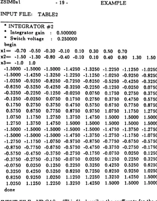
Integrator gain 0.1•
Switch voltage 2.5 beginxl= -2.5 -1.75 -1.0 -0.5 -0.1 0.1 0.5 1.0 1.75 2.5 x2= ..1.5 ..1.2 -0.9 -0.6 -0.3 0.3 0.6 0.9 1.2 1.5 x3= ..1 1
-1.5 -1.425 -1.35 -1.3 -1.26 -1.24 -1.2 -1.15 -1.075 -1.0 -1.2 -1.125 -1.05 -1.0 -0.96 -0.94 -0.9 -0.85 -0.775 -0.7 -0.9 -0.825 -0.75 -0.7 -0.66 -0.64 -0.6 -0.55 -0.475 -0.4 -0.6 -0.525 -0.45 -0.4 -0.36 -0.34 -0.3 -0.25 -0.175 -0.1 -0.3 -0.225 -0.15 -0.1 -0.06 -0.04 0.0 0.05 0.125 0.2 003 0.375 0.45 0.5 0.54 0.56 0.6 0.65 0.725 008 0.6 0.675 0.75 0.8 0.84 0.86 0.9 0.95 1.025 1.1 0.9 0.975 1.05 1.1 1.14 1.16 1.2 1.25 1.325 1.4 1.2 1.275 1.35 1.4 1.44 1.46 1.5 1.50 1.500 1.5 105 1.500 1.50 1.5 1.50 1.50 1.5 1.50 1.500 1.5 -1.5 -1.500 -1.50 ..1.5 -1.50 -1.50 ..1.5 -1.50 -1.500 ..1.5 -1.5 -1.500 -1.50 -1.5 -1.46 -1.44 -1.4 .,,1.35 ..1.275 -1.2 -1.4 -1.325 -1.25 -1.2 -1.16 -1.14 -1.1 ..1.05 -0.975 -0.9 -1.1 -1.025 -0.95 -0.9 -0.86 -0.84 -0.8 -0.75 -0.675 -0.6 -0.8 -0.725 -0.65 -0.6 -0.56 -0.54 -0.5 -0.45 -0.375 -0.3 -0.2 -0.125 -0.05 0.0 0.04 0.06 0.1 0.15 0.225 0.3 0.1 0.175 0.25 0.3 0.34 0.36 0.4 0.45 0.525 0.6 0.4 0.475 0.55 0.6 0.64 0.66 0.7 0.75 0.825 0.9 0.7 0.775 0.85 0.9 0.94 0.96 1.0 1.05 1.125 1.2 1.0 1.075 1.15 1.2 1.24 1.26 1.3 1.35 1.425 1.5 done
* INTEGRATOR # 2
•
Integrator gain 0.50* Switch voltage 0.25 begin
x1= -1.5 -1.2 -0.9 -0.6 -0.3 0.3 0.6 0.9 1.2 1.5
x2= -1.5 -1.2 -0.9 -0.6 -0.3 0.3 0.6 0.9 1.2 1.5
x3= -1 1
-1.500 -1.500 -1.500 -1.500 -1.500 -1.225 -1.075 -0.925 -0.775 -0.625
-1.500 -1.500 -1.500 -1.375 -1.225 -0.925 -0.775 -0.625 -0.475 -0.325 -1.500 -1.375 -1.225 -1.075 -0.925 -0.625 -0.475 -0.325 -0.175 -0.025
-1.225 -1.0i5 -0.925 -0.775 -0.625 -0.325 -0.175 -0.025 0.125 0.275 -0.925 -0.775 -0.625 -0.475 -0.325 -0.025 0.125 0.275 0.425 0.575
-0.325 -0.175 -0.025 0.125 0.275 0.575 0.725 0.875 1.025 1.175
0.025 0.125 0.275 0.425 0.575 0.875 1.025 1.175 1.325 1.475 0.275 0.425 0.575 0.725 0.875 1.175 1.325 1.475 1.500 1.500
0.575 0.725 0.875 1.025 1.175 1.475 1.500 1.500 1.500 1.500 0.875 1.025 1.175 1.325 1.475 1.500 1.500 1.500 1.500 1.500
-1.500 -1.500 -1.500 -1.500 -1.500 -1.475 -1.325 -1.175 -1.025 -0.875
-1.500 -1.500 -1.500 -1.500 -1.475 -1.175 -1.025 -0.875 -0.725 -0.575
-1.500 -1.500 -1.475 -1.325 -1.175 -0.875 -0.725 -0.575 -0.425 -0.275
-1.475 -1.325 -1.175 -1.025 -0.875 -0.575 -0.425 -0.275 -0.125 0.025
-1.175 -1.025 -0.875 -0.725 -0.575 -0.275 -0.125 0.025 0.175 0.325
-0.575 -0.425 -0.275 -0.125 0.025 0.325 0.475 0.625 0.775 0.925
-0.275 -0.125 0.025 0.175 0.325 0.625 0.775 0.925 1.075 1.225
0.025 0.175 0.325 0.475 0.625 0.925 1.075 1.225 1.375 1.500
0.325 0.475 0.625 0.775 0.925 1.225 1.375 1.500 1.500 1.500
0.625 0.775 0.925 1.075 1.225 1.500 1.500 1.500 1.500 1.500
done
Output
1.50
I
1.50
Input Value -2.5 -1.75 -1.0
-0.5 0001 0.1 0.5 1.0 1075 2.5
I
1.00
I
.500
I
o o
1.00
.500
-1.50~ I · i -+- ....-· t - - t
--1.50 -1.00 -.500
-1.00 -.500
1.50 1.00
.500
o
-.500 -1.00
o
1.00 1.50
.500
-1.00 -.500
-1 •50
+M-~====-~--1.50
Initial Value
1.50
Output
1.50
Input Value
-1.5
-1.2 -o.o
-0.6 -0.3 0.3
0.6
O.g
1.2
1.5
1.00
.500 o
-.500 -1.00
1.00
o
.500
-.500
-1.00
-1.50 ,...---.-::.;;,----'" -1.50
1.50
1.50 1.00
.500 o
-.500
-1.00
o
1.00
.500
-.500
-1.00
-1. 50 ~--==-'-'--
...
~----1.50
Initial Value
4.1.2.1. Baseband Spectrum
Simulations were performed for two cases - an input amplitude of -15 dB
(with respect to the comparator reference 2.5V) and the maximum amplitude of 0
dB. Operation of the integrators for -15 dB is basically in the linear region and no
limiting occurs. However, limiting does occur in the integrators for a 0 dB input
amplitude.
Figure 4.6 shows the baseband spectra for a -15 dB input amplitude. The
table method simulations closely match the results using a difference equation.
Spectrum,
dB
25.0
o
Difference Equation --- Table
-25.0
-50.0
,
\ \
\ . ,
,
,,..\ \
3.50 4.00 3.00
2.50 2.00
1.50
1.00
.500
-1OO~----:::t:-:---~-t-:---t:----+- -+- -+- ~_
_-':""-+-o
-75.0
Frequenc~,
KHz
The slight deviations may be due to the limited accuracy of the table storage. This
accuracy can be improved by extending the length of the precision of the data.
The baseband spectra for a 0 dB input amplitude is shown in Figure 4.7. The table result is close to the difference equation spectrum with some deviation in
power across the band. Distortion components are present in both methods, but
with some difference in level. The difference in levels can be attributed to pure hard limiting in the direct difference equation as compared to softer limiting in the tables. The latter is caused by interpolation between the linear and saturation
regions given a finite number of table points. Since a pure hard limiter does not
Spectrum~
dB
40.0
20.0
o
- - - Difference Equation
--- Table
\ \
\
-20.0
-40.0
-60.0
,
\
\-,-
.,
...--
,'-_...
.500 .1.:.00 1.50 2.00 2.50 3.00 3.50 4.00
Frequenc~ ~ KI--1z
4.1.2.2. Signal-to-Distortion Ratio
Table 4.1 compares the signal-to-distortion ratio (distortion includes noise
plus total harmonic distortion) for both methods of simulation. The
SnR
as afunction of input amplitude is plotted in Figure 4.8. Close agreement is obtained
at low signal levels whereas deviations at large signal levels occur due to integrator
saturation, as described earlier. Figure 4.9 is a plot of the differences in SDR for
the two simulation methods. Notice that this difference is highly random. The
slight differences are attributed to the accuracy of the interpolation routine and
the finite precision of the Fourier transform routine. Better accuracy can be
Table 4.1: SDR summary for ideal table and difference equation simulations
Diff. Ideal Diff. Ideal Diff. Ideal
Input Equat. Table Input Equat. Table Input Equat. Table
0 40.9661 40.5639 -11 71.8130 70.8580 -25 56.8837 57.6987
-1 65.5709 65.2184 -12 70.2594 70.4663 -28 53.0780 52.6831 -2 71.8916 72.8751 -13 67.6239 69.4333 -30 52.4806 53.3591
-3 73.1701 73.7618 -14 69.2771 68.6706 -33 48.6391 51.1124 -4 75.4289 74.4117 -15 67.3672 67.1737 -35 48.2805 47.3207
-5 72.8379 73.6041 -16 66.2523 66.5136 -38 44.9667 45.3714
-6 73.5745 74.7970 -17 67.1231 66.3335 -40 42.7303 43.0408
-7 74.9449 73.1008 -18 65.8062 64.4709 -45 36.2685 38.0489
80.0
dB
70.0
60.0
50.0
40.0
30.0 - - - Difference Equation
--- Table
o
-10.0 -20.0
-30.0 -40.0
-50.0
20. O'
-t---t---t---+---+---+---__
__+_
-60.0
Amplitude~
dB
o
-10.0 -20.0
-30.0 -40.0
-50;0 1.00
dB
2.00
-2. OO-+-- -+- --+- ---1 ~-.¥----_+_---__&_
-60.0 -1.00
Amplitude~
dB
Figure 4.9: SDR differences (difference equation-table) versus input amplitude
4.1.2.3. Interpolation Accuracy
The interpolation errors in the above example can be understood by consider-ing two cases with the integrator operatconsider-ing in the linear region and in the
satura-tion region. Table 4.2 is a summary of interpolation and difference equation results for a specific clock cycle during a simulation using an input signal level of 0 dB. The first integrator is operating in the linear region whereas the second integrator is operating in the saturation region. The interpolation output is taken directly from a node voltage listing and the difference equation output is calculated using Equation 3.1. Recall that the reference voltage is 2.5 V for the first
integra-tor and 0.25 V for the second integraintegra-tor. Notice that for the first integraintegra-tor the
interpolation routine generates an output value that is exactly as calculated by the
difference equation. This result is as expected since the integrator operation is
linear and the interpolation routine is linear. However, the interpolated result for
the second integrator is slightly different. The result given is the exact answer to
Table 4.2: Summary of integrator simulation for cycle #249
INTEGRATOR
#
1Interpolation formula Difference equation
INTEGRATOR
#2
Interpolation formula Difference equation
0.619197 0.619197
the difference oquntion, although a hard limit of 1.5 V was speeifled, ann 1.5 V
would be the actual result. For this specific cycle a 4.3
%
difference exists betweenthe table result and the difference equation saturation level. In effect, the
interpo-lation scheme sees the saturation earlier than it actually occurs. Therefore, a soft
limiting effect is introduced into the integrator. The overall performance of the
delta-sigma modulator is not degraded to a large extent, however, as shown in the
previous section.
402.
LOW-LEVEL BENCHMARK
4.2.1. ISDN Circuit
This section considers a delta-sigma modulator system for use in ISDN
appli-cations. The connectivity of the circuit is the same as in the previous example (see Figure 4.1) except that an IIR filter is not used. A second-order delta-sigma
modu-lator is chosen with <Xl
=
0.1 and <X2=
0.5 and ~l = 0.1. The selection of ~l insures that the range of voltages at both inputs of the second integrator areequivalent. The sampling frequency is f8
=
5.12MHz.
The decimation filter hasparabolic weighting with 128 taps, and the sampling rate is reduced by a factor of
M = 32 to 160 kHz with an 80 kHz baseband frequency. For the benchmark study, the modulator input is a 30 kHz sinewave.
Figure 4.10 shows the second-order switched-capacitor circuit designed to
3 pF
2pF
t1J, •3 pF «b•
~-rr
4>. 1 pF ~,r
3 PF-rT
Comparatorr
3pFclJ. .3 pF 4»,
-rT
4», .J pF 4tl
rT
In.erter Inverter FF
Clock
Figure 4.10: Second-order delta-sigma switched-capacitor circuit
insures that its transfer function is independent of parasitic capacitances between any node and ground [33,34]. The comparator is ideal whereas the operational
amplifiers are not; a class AB op-amp (schematic in Appendix B) is designed for a 1.0
urn
CMOS process. <lJ1 and <1>2 are nonoverlapping clocks, each with a duty cycle close to 50 percent. Integrator#1
's output is stable at the end of <1)1 andIntegrator #2's output is valid at the end of c)2. Note that the clock timing causes
the first integrator to be a summing integrator with negative gain and the second