complex modules in one chip. As number of modules per chip is increasing, number of transistors in a chip increases resulting in increase in area and power dissipation. Area and power dissipation problems can be most effectively addressed if the basic building blocks of the circuit are designed for lower power dissipation and occupy less space. Flip-Flop, which is basic building block, plays a major role in design of complex systems. From the open literature, C2MOS Flip-Flop and PowerPC 603 Flip-Flops are classic structures that dissipate less power. In this paper, two new low power dissipating Flip-Flop architecture are proposed and compared with conventional Flip-Flops. In the proposed Flip-Flop architectures, power dissipation is reduced up to 30% to 40% compared with conventional Flip-Flops and area is also reduced. Johnson counter is designed with the proposed Flip-Flops which exhibit low power dissipation. The simulation is done in MENTOR GRAPHICS, Schematic editor, Generic GDK, 130nm technology.
Keywords— Power dissipation, Flip-Flop, C2MOS, PowerPC 603, Johnson counter.
I. INTRODUCTION
With the widespread use of mobile devices in modern society, power efficiency and energy savings become extremely important issues for designers. CMOS has been the dominant technology for VLSI implementations. As VLSI circuits continue to grow and technologies evolve, the level of integration is increased and higher clock speeds are achieved. Higher clock speeds, increased levels of integration and technology scaling are causing unabated increases in power consumption. As a result, low power consumption [1-3] is becoming a critical issue for modern VLSI circuits. Furthermore, power dissipation, dynamic and static, has become a limiting factor for transistor performance, long term device reliability, and increasing integration.
Flip-Flops, which is a basic building block of many electronic circuits that stores a logical state of one or more data in response to a clock pulse. Flip-Flops are often used in computational circuits to operate in selected sequences during recurring clock intervals to receive and maintain data for a limited time period. At each rising orfalling edge of a clock signal, the data stored in Flip-Flops can be applied as inputs to other combinational or
been the integral part of many digital systems to construct the sequential part of it. To achieve low power dissipation along with area efficiency, two new D Flip-Flop architectures are proposed and are compared with the conventional Flip-Flops.
II. POWER DISSIPATION
The design of portable devices requires consideration for peak power consumption to ensure reliability and proper operation. However, the time averaged power is often more critical as it is linearly related to the battery life. There are four sources of power dissipation in digital CMOS circuits: switching power, short-circuit power, leakage power and static power. The following equation describes these four components of power:
Pavg = αCLVddVsfck+IscVdd + IleakageVdd + IstaticVdd (1)
Here Pstatic = αCLVddVsfck , Pdynamic = IscVdd ,
Pleakage= IscVdd
and Pshort-circuit = IstaticVdd .
III. CONVENTIONAL FLIP-FLOPS
A. C2MOS FLIP-FLOP
The C2MOS Flip-Flop [5] is a pseudo-static Flip-Flop, which is obtained by the addition of a weak C2MOS feedback at the outputs of the master and the slave latches in a dynamic C2MOS Flip-Flop as shown in the Fig. 1. When the clock is at logic ‘high’, the clocked inverter CLKI1 latches the input at D to an intermediate node N. The feedback consisting of clocked inverter CLKI2 and inverter I1 maintains this logic level at node N when clock is at logic ‘HIGH’. Similarly when CLK changes to logic ‘LOW’, the slave latches gets functional and clocked inverter CLKI4 and inverter I2 maintains this logic level at output Q when clock is grounded. There is no Vt-drop at
intermediate circuit nodes.
.
Fig. 1 C2MOS Flip-Flop
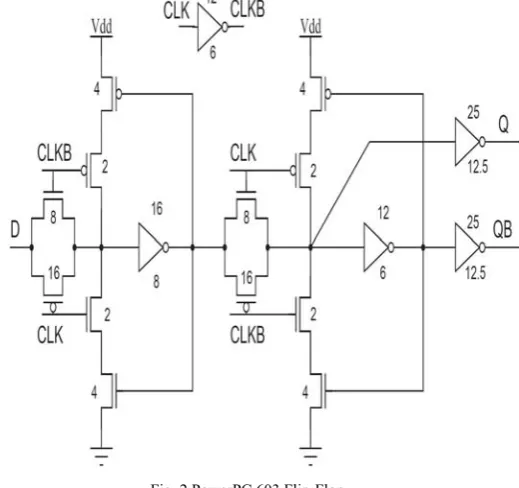
B. POWERPC 603 FLIP-FLOP
Power PC means Performance Optimization with Enhanced RISC Performance Computing. The power dissipation is low and also having low clock-to output (CLK-Q) delay. In synchronous systems, the latching elements have the delay overhead which is expressed by the data-to-output (D-Q) delay rather than CLK-Q delay. Here, D-Q delay is the combination of CLK-Q delay and the setup-time of the Flip-Flop. But the static designs lack the low D-Q delay due to their large positive setup-time, and also most of them are susceptible to flow through resulting from CLK overlap.
The PowerPC 603 master-slave [6] latch in Gerosa et al.’s experiment is shown in Fig. 2. It has the advantages of having a low-power keeper structure and a low latency direct path. It is one of the fastest classical structures and its main advantage is the short direct path and low power feedback. The large load on the clock will greatly affect the total power consumption of the Flip-Flop. This Flip-Flop is the transmission gate Flip-Flop, it has a fully static master– slave structure, which is constructed by cascading two identical pass gate latches and provides a short clock to output latency. It does have a worse data-to-output latency because of the positive setup time and its sensitivity to clock signal slopes and data feed through is another concern when using it. The large D-Q delay resulting from the positive setup time is one of the disadvantages of this design. Also, the large data and CLK node capacitances make the design inferior in performance. Despite all these shortcomings, static designs still remain as the low power solution when the speed is not a primary concern
.
Fig. 2 PowerPC 603 Flip-Flop
IV.PROPOSEDFLIP-FLOP ARCHITECTURES
A. Proposed model –I
The proposed model-I is the modified version of PowerPC 603 which acts like a static Flip-Flop as shown in the Fig. 3. It uses a low-power keeper [7] structure in the master and slave mode. In the proposed model- I the master mode is modified. Because of the drop due to the threshold of the transistors, PowerPC 603 suffers with short circuit power dissipation. An NMOS transistor with complemented clock signal is used to make feedback path functional only during OFF cycle of the clock. This reduces short circuit current during ON cycle. To reduce the number of transistor, only NMOS transistor is used in master latch as shown in Fig. 3. If PMOS transistor with clock signal is used in feedback, the logic level at the node X would be maintained when the clock is in the logic level ‘HIGH’ rather than the logic level ‘LOW’. Hence, when the clock is stopped (grounded), the circuit would show a dynamic behaviour instead of static behaviour. This limitation is overcome by using a NMOS transistor in feedback instead of PMOS transistor.
Fig. 3 Proposed Model-I Flip-Flop
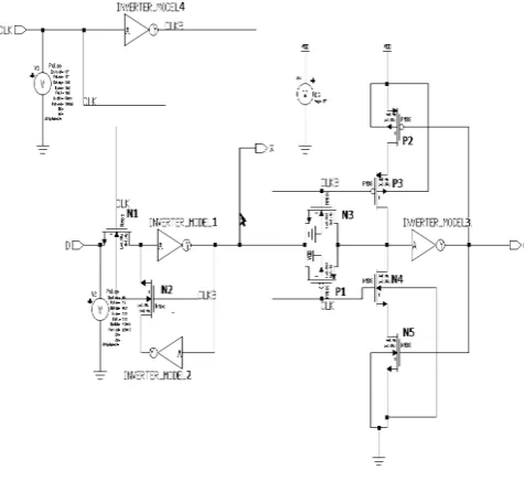
B. Proposed model –II
The proposed model-II is the modified version of proposed model-1. In the proposed model –II shown in Fig. 4, the transmission gate is replaced with nMOS. Since the circuit is operated as master-slave. The slave is disconnected from the master when the clock is high. By using nMOS (N3) as a path, the average power dissipation is improved by 20%. When the slave is disconnect from the master, the N4 and N5 in the power keeper provides the feedback and ensures that the data is retained till the next clock cycle.
In digital logic and computing, a counter is a device which stores the number of times a particular event or process has occurred, often in relationship to a clock. Among different types of counters, Johnson counter needs half the number of Flip-Flops.
Johnson counter requires a reset to initialize the count. So the proposed model-II is modified as shown in the Fig.5
Fig. 4 Proposed Model-II Flip-Flop
Fig. 5 Proposed Model-II Flip-Flop with reset
A Johnson up-down counter is designed with modified version of proposed model –II. The architecture of Johnson counter is shown below Fig. 6.
Fig. 6 Johnson up-down Counter architecture using Proposed model-II
V. RESULTS
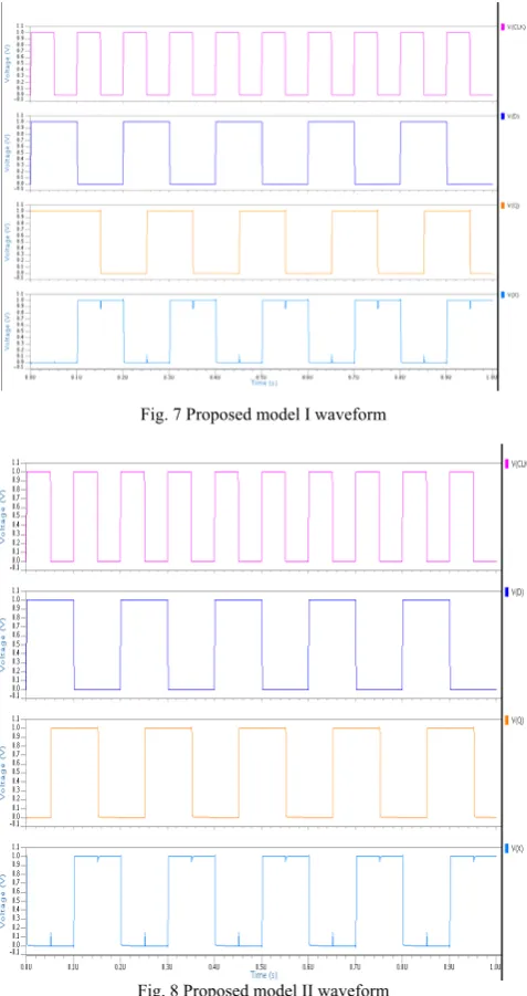
Simulation are carried out using MENTOR GRAPHICS, generic GDK, 130-nm CMOS technology at nominal conditions with clock frequency 10MHz. The simulated waveform of the Proposed Model –I Flip-Flop is shown in Fig. 7. As the circuit works like a master-slave Flip-Flop the data D is provided at the output Q only in the negative half cycle of the clock. This reduces the Race through problem. The average power dissipation and area required is reduced compared to PowerPC 603 Flip-Flop.
Fig. 7 Proposed model I waveform
Fig. 8 Proposed model II waveform
The performance comparisons of the Flip-Flops are given in the Table I.
TABLE –I
PERFORMANCECOMPARISONOFVARIOUSFLIP-FLOPS
Flip-Flop Power Dissipation(pW)
No. of transistors
C2MOS 815.0527 20
PowerPC 603 925.0929 18
Proposed model –I 763.7391 14
Proposed model-II 583.1645 13
Proposed model-II with reset 582.113 14
The proposed models exhibits up to 30% reduction in total power dissipation and area compared to C2MOS and PowerPC 603 Flip-Flop.
Since proposed model – II exhibits less power dissipation and area efficient, A Johnson counter [8] is designed with the Proposed Model-II, the waveform shown
Fig. 9 Johnson counter waveform designed with Proposed model II
The performance comparisons of the Johnson counter with conventional and proposed Flip-Flops are given in the table II.
TABLE-II
PERFORMANCE COMPARISON OF JOHNSON COUNTERS WITH DIFFERENT FLIP-FLOPS
Flip-Flop Power Dissipation(nW)
C2MOS 3.7
PowerPC 603 3.2
Proposed model –I 3.05
Proposed model-II (with reset) 2.547
VI.CONCLUSION
Sanchez, P. Ippolito, N. Tai, S. Litch, J. Eno, J. Golab, N. Vanderschaaf, and J. Kahle, “A 2.2 W, 80 MHz superscalar RISC microprocessor,” IEEE J. Solid-State Circuits, vol. 29, no. 12, pp. 1440–1452, Dec. 1994.
[7] J. Kao and A. Chandrakasan, "MTCMOS sequential circuits," Proceedings of European Solid State Circuits Conference, pp 332- 335, September 2001.
[8] Low-power dual dynamic node pulsed hybrid Flip-Flop featuring efficient embedded logic ,kalarikkal absel, lijo manuel, and R. K. Kavitha, member, IEEE, IEEE transactions on very large scale integration (vlsi) systems, vol. 21, no. 9, September 2013.
[9] Peiyi Zhao, Jason McNeely, WeidongKuang, Nan Wang, and Zhongfeng Wang “Design of Sequential Elements for Low Power Clocking System” IEEEtransactions on Very Large Scale Integration (VLSI) systems, vol. 19, no. 5, May 2011