Reseeding LFSR for Test Patterns
Generation
Injeti Salomi1,S. Ashok Reddy2
1
P.G. Scholar, 2Head of the Department, M.Tech.,
1,2
Electronics and Communication Engineering
1,2
Geethanjali College of Engineering and Technologies ( Formerly AVR & SVR Engineering College ) Email: [email protected], [email protected]
Abstract
Testing of circuits got troublesome as the size of coordination is expanding as said in Moore's Law. Ordinary testing approach isn't adequate with the development of gadget tallies and thickness. Testing causes the designer to examine shortcomings and blunder present in created circuit which serves to lessen time require to test and in this manner diminishes odds of getting fizzled during activity. Test time is one of the most significant boundaries in advanced circuit testing which impacts the generally speaking procedure of testing. Diminishing the test time of the test design age is one of the most affected answer for the process. Reseeding LFSR is one of the strategies to produce the test designs for testing. In this paper, pseudo-arbitrary test designs are created to test circuit utilizing reseeding LFSR method. This assists with decreasing the test design required to be put away for testing. This method can be applied with the standards which are required for low force just as low test data volume. Issue inclusion of proposed circuit is determined utilizing
ISCAS'89 benchmark circuits. The
procedure is coordinated with the
benchmark circuits and examination is finished in view of the exhibition and asset
usage. Proposed model lessens the
requirement for memory to store seed esteem and the power usage. Reseeding can basically be applied for BIST which targets total issue inclusion and minimization of the
test length. Data pressure for lessening the test design required for testing will in a roundabout way lessen the time required to check the circuits. Future work is to lessen time required for the test design age. Hamming separation can be applied to ascertain the quantity of bits changing during the test designs progress. Hamming separation approach can be executed to lessen the boundary.
Keywords: Index Terms—Automatic Test Pattern Generation, Reseeding LFSR, Circuit Under Test, Fault Coverage.
INTRODUCTION
platform based approach. For example, the platform FPGAs such as Xilinx Virtex II Pro and Altera Excalibur include custom designed fixed programmable processor cores together with millions of gates of reconfigurable logic devices. In addition to this, the development of Intellectual0 Property (IP) cores for the FPGAs for a variety of standard functions including processors, enables a multimillion gate .FPGA to be configured to contain all the components of a platform based FPGA. Development tools such as the Altera System-On-Programmable Chip (SOPC) builder enable the integration of IP cores and the user designed custom blocks with the Nios II soft-core processor. Soft-core processors are far more flexible than the hard-core processors and they can be enhanced with custom hardware to optimize them for specific application. Power dissipation is a challenging problem for today’s System-on-Chips (SOCs) design and test. In general, the power dissipation of a system in test mode is more than in normal mode. Four reasons are blamed for power increase during test.
• High switching activity due to nature of test patterns
• Parallel activation of internal cores during test
• Power consumed by extra design-for-test(DFT) circuitry
• Low correlation among test vectors
This extra average and peak power consumption can create problems such as instantaneous power surge that cause circuit damage, formation of hot spots, difficulty in performance verification, and reduction of the product field and life time[4]. Thus special care must be taken to ensure that the power rating of circuits is not exceeded during test application. Different types of techniques are presented in the literature to control the power consumption. These
mainly includes algorithms for test
scheduling with minimum power,
techniques to reduce average and peak power, techniques for reducing power during scan testing and
BIST(built-in-selftest) technique. Since off-chip
communication between the FPGA and a processor is bound to be slower than onchip communication, in order to minimize the time required for adjustment of the parameters, the built in self test approach using design for testability technique is proposed for this case.
LITERATURE SURVEY
Different techniques are available to reduce the switching activities of test pattern, which reduce the power in test mode. For linear feedback shift register (LFSR), Giard proposed a modified clock scheme in which only half of the D flip-flops works, thus only half of the test pattern can be switched. S.K. Guptha proposed a BIST TPG for low switching activity in which there is d-times clock frequency between slow LFSR and normal LFSR and thus the test pattern generated by original LFSR is rearranged to reduce the switch frequency. LT-TPG is proposed to reduce the average and peak power of a circuit during test. The above said techniques can reduce the average power compared to traditional linear feedback shift register (LFSR). A better low power can be achieved by using single input change pattern generators. It is proposed that the combination of LFSR and scan shift register is used to generate random single input charge sequences. it is proposed that (2m-1) single input change test vectors can be inserted between two adjustment vectors generated by LFSR, m is length of LFSR. it is proposed that 2m single input changing data is inserted between two neighboring seeds. The average and peak power are reduced by using the above techniques. Still, the switching activities will be large when clock frequency is high.
In CMOS technology, the power dissipation can be classified into static and dynamic. Static power dissipation is mainly due to the leakage current. Dynamic power dissipation is due to switching transient current and
charging and discharging of load
capacitances. Some significant parameters for evaluating the power consumption of CMOS circuits are discussed below.
Ei = 1/2Vdd2C0FiSi (1)
Where Vdd is the supply voltage, C0 is the load capacitance. The product of Fi and Si is called weighted switching activity of internal circuit node i. The average power consumption of internal circuit node I can be given by,
Pi =1/2 Vdd2C0FiSi f (2)
f is the clock frequency .The summary of Pi of all the nodes is named as average power consumption. It can be observed from (1) and (2) that the energy and power consumption mainly depends on the switching activities, clock frequency and supply voltage. This paper reduces the switching activity at the inputs of the circuit under test (CUT) as low as possible.
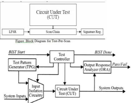
BIST approach: INTRODUCTION
The various test structures are proposed for BIST techniques. A typical structure used for gene-ration of pseudo-random test sets is the linear feedback shift register (LFSR). The BIST techniques have wide application in testing whole devices and embedded components. Built-in self-test (BIST) is a
set of structured-test techniques for
combinational and sequential logic,
memories, multipliers, and other embedded logic blocks. In each case the principle is to generate test vectors, apply them to the circuit under test (CUT) or device under test (DUT), and then check the response [27]. BIST USING LFSR AND SIGNATURE ANALYZER
At the heart of this BIST approach, lie a pseudo-random binary sequence (PRBS) generator and a signature register. The PRBS generator is most easily implemented using a linear feedback shift register
(LFSR). A PRBS generator allows us to generate all (well, almost all) of the required binary patterns for the circuit under test. The LFSR can be used to both generate the test sequence for the design that is to
incorporate BIST and with slight
modification can be used to capture the response of the design and generate a signature (the bit pattern held in the signature register).One approach for built-in self-test (BIST) of circuits with scan is to use a linear feedback shift register (LFSR) to shift a pseudo-random sequence of bits into the scan chain. When a pattern has been shifted intothe scan chain, it is applied to the circuit-under-test (CUT) and the response is loaded back into the scan chain and shifted out into a signature register for compaction as the next pattern is shifted into the scan chain.
controller provides a control signal to activate all the blocks.
BIST has some major drawbacks where architecture is based on the linear feedback shift register[LFSR].The circuit introduces more switching activities in the circuit under test (CUT)during test than that during normal operation. It causes excessive power dissipation and results in delay penalty into the design.
Classification of test strategies:
1.Weighted Pseudorandom: Testing:
In weighted pseudorandom testing, pseudorandom patterns are applied with certain 0s and 1s distribution in
order to handle the random pattern resistant fault undetectable by the pseudorandom testing. Thus, the test length can be effectively shortened.
2.Pseudo exhaustive Testing:
Pseudo exhaustive testing divides the
CUT into several smaller sub circuits and tests each of them exhaustively. All detectable flaws within the sub circuits can be detected. However, such a method involves extra design effort to partition the circuits and deliver the test patterns and test responses. BIST is a set of
structured-test techniques for
combinational and sequential logic,
memories, multipliers, and other
embedded logic blocks. BIST is the commonly used design technique for self testing of circuits.
3.Pseudorandom Testing:
Pseudorandom testing involves the
application of certain length of test patterns that have certain randomness property. The test patterns are sequenced in a deterministic order. The test length and the contents of the patterns are used to impart fault coverage.
4.Exhaustive Testing:
Exhaustive testing involves the
application of all possible input
combinations to the circuit under test (CUT). It guarantees that all detectable faults that divert from the sequential behavior will be detected. The strategies
are often applied to complex and well isolated small modules such as PLAs.
5.Stored Patterns:
Stored-pattern approach tracks the
pregenerated test patterns to achieve certain test goals. It is used to enhance system level testing such as the power-on
self test of a computer and
microprocessor functional testing using micro programs
BLOCK DIAGRAM FOR BIST:
It shows the block diagram for BIST using 10-bit maximal length LFSR and 10-bit signature register. Here clock is available all the time for the circuit operation .Here if reset is “1” the circuit stay in its previous state, however if reset is “0” then it start operation.
CIRCUIT DIAGRAM:
Reseeding LFSR
LFSR (Linear Feedback Shift Register) one type of shift register whose input is linear function of its previous bit. Some of the applications of LFSR are, counters, pseudo random pattern generation, pseudo-noise sequences and whitening sequences. Implementation of LFSR also includes the XOR gates connected in series with series of D flipflops or XOR connected externally. The XOR connected externally called as type 1 LFSR and XOR connected internally called type 2 LFSR. Single bit linear shift register is XOR shift register whose input bits are guided by the exclusive or (XOR) which flops the overall register value. Basic value applied to LFSR is called as seed and thus the value givenby the shift register is completely determined. Seed value is used to generate required test patterns and required test cubes. Basic idea of LFSR is to generate different test cases by changing seed value. A seed is a basic state of the LFSR that is expanded while running the LFSR in sovereign mode. Periodic sequence generated from the LFSR should start from non-zero state. Maximum length of seed value given by formulae: 2n-1.
Consider AND gate which has n input lines which is given in Fig. 2. The probability of getting bit 1 at the output of the AND gate is 0.5n when unbiased random inputs are applied.
It becomes impossible to determine the stuck at 0 fault if 0 is applied at the input
side. It is not possible to recognize the stuck -at 0 faults present in the circuit or AND gate. So, it is difficult to detect the such type of fault from the test pattern generated. Such a fault is called a RPRF (Random Pattern Resistant Fault).
A. Pseudo Random Number Generator
LFSR uses random numbers and used widely for random process. George Marsaglia’s Diehard tests are used to generate pseudo random numbers.
Randomness means that the next value which is generated is unpredictable. Encryption algorithms and security protocols are based on random number generators. The system uses the primitive polynomial to generate random sequence. Primitive polynomial used in the proposed system is of degree 4:
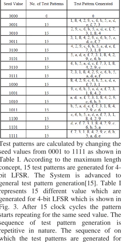
Test patterns are calculated by changing the seed values from 0001 to 1111 as shown in Table I. According to the maximum length concept, 15 test patterns are generated for 4- bit LFSR. The System is advanced to general test pattern generation[15]. Table I represents 15 different value which are generated for 4-bit LFSR which is shown in Fig. 3. After 15 clock cycles the pattern starts repeating for the same seed value. The sequence of test pattern generation is repetitive in nature. The sequence of on which the test patterns are generated for seed values are same only the starting value will be different.
The architecture is used to test circuits using less storage and time. Architecture consist of reseeding LFSR and counter. Counter will count till the required value for which the user wants to generate test patterns. For example, for generating test patterns for n bit inputs the counter should count the value till 2n-1 according to the maximum length formulae which are used to produce the automatic generation of seed continuously which are fed to reseeding
LFSR to generate required pseudo-random test patterns which will be provided to circuit under test. The output of the CUT will be compared with the output of the
correctly tested circuits which are stored in ROM called as golden signature using signature analysis. Fig.4. shows the proposed architecture which consist of counter and reseeding LFSR. Counter is used in the system to produce the seed value. The seed value generated should be stable for 2n-1 clock cycle. In the proposed system the circuit can work up to 32 bits [4]. The system can accept the input value up to 32 bits. So, one value of the counter should be stable for 232-1 number of clock cycle. Counter 1 and counter 2 is compressed in single block named counter as shown in Fig 4.
LFSR and are given to CUT. The schematic diagram of the proposed system is shown in Fig. 5. The time required to generate test patterns are calculated as shown in Fig. 6. The setup slack is 1.801ns and hold slack is -0.535ns is observed from the simulated proposed circuit time report shown in Fig. 6. System consumes about 0.248W power generated from the Xillinx Vivado tool.
The proposed method is completed using verilog code simulated in Questa Sim and it is tested with ISCAS’89 benchmark circuits scan based design. Consider 1010 as the initial value given to LFSR register. More faults are likely to be detected with the circuits. To get shorter test which is given by test length, highest time response is achieved for the unspecified values on scanned chain such that it is not specified on unscanned state variable.
INTRODUCTION TO VLSI
Very-large-scale integration (VLSI) is the process of creating integrated circuits by combining thousands of transistor-based circuits into a single chip. VLSI began in the 1970s when complex semiconductor and communication technologies were being developed. The microprocessor is a VLSI device. The term is no longer as common as it once was, as chips have increased in complexity into the hundreds of millions of transistors.
5.1 Overview:
The first semiconductor chips held one transistor each. Subsequent advances added more and more transistors, and, as a consequence, more individual functions or systems were integrated over time. The first integrated circuits held only a few devices, perhaps as many as ten diodes, transistors, resistors and capacitors, making it possible to fabricate one or more logic gates on a single device. Now known retrospectively
as "small-scale integration" (SSI),
improvements in technique led to devices
with hundreds of logic gates, known as large-scale integration (LSI), i.e. systems with at least a thousand logic gates. Current technology has moved far past this mark and today's microprocessors have many millions of gates and hundreds of millions of individual transistors.
At one time, there was an effort to name and calibrate various levels of large-scale integration above VLSI. Terms like Ultra-large-scale Integration (ULSI) were used. But the huge number of gates and transistors available on common devices has rendered such fine distinctions moot.
Terms suggesting greater than VLSI levels of integration are no longer in widespread use. Even VLSI is now somewhat quaint, given the common assumption that all microprocessors are VLSI or better.
As of early 2008, billion-transistor processors are commercially available, an example of which is Intel's Montecito Itanium chip. This is expected to
become more commonplace as
semiconductor fabrication moves from the current generation of 65 nm processes to the next 45 nm generations (while experiencing new challenges such as increased variation across process corners). Another notable example is NVIDIA’s 280 series GPU.
This microprocessor is
unique in the fact that its 1.4 Billion transistor count, capable of a teraflop of performance, is almost entirely dedicated to logic (Itanium's transistor count is largely due to the 24MB L3 cache). Current designs, as opposed to the earliest devices, use extensive design automation and automated logic synthesis to lay out the transistors, enabling higher levels of
complexity in the resulting logic
functionality. Certain high-performance
breaking established design rules to obtain the last bit of performance by trading stability).
What is VLSI?
1.1. VLSI stands for "Very Large Scale Integration". This is the field which involves packing more and more logic devices into smaller and smaller areas.
VLSI
Simply we say Integrated circuit is many transistors on one chip.
Design/manufacturing of extremely
small, complex circuitry using
modified semiconductor material
Integrated circuit (IC) may contain
millions of transistors, each a few mm in size
Applications wide ranging: most
electronic logic devices
2.5.3 History of Scale Integration:
late 40s Transistor invented at Bell
Labs
late 50s First IC (JK-FF by Jack Kilby
at TI)
early 60s Small Scale Integration (SSI)
10s of transistors on a chip
late 60s Medium Scale
Integration (MSI)
100s of transistors on a chip
early 70s Large Scale Integration (LSI)
1000s of transistor on a chip
early 80s VLSI 10,000s of transistors
on a
chip (later 100,000s & now 1,000,000s)
Ultra LSI is sometimes used for
1,000,000s
SSI - Small-Scale Integration (0-102)
MSI - Medium-Scale Integration
(102-103)
LSI - Large-Scale Integration (103-105)
VLSI - Very Large-Scale Integration
(105-107)
ULSI - Ultra Large-Scale Integration
(>=107)
Advantages of ICs over discrete
components:
While we will concentrate on
integrated circuits , the properties of integrated circuits-what we can and cannot efficiently put in an integrated circuit-largely determine the architecture of the entire system. Integrated circuits improve system characteristics in several critical ways. ICs have three key advantages over
digital circuits built from discrete
components:
Size. Integrated circuits are much
smaller-both transistors and wires are shrunk to micrometer sizes, compared to the millimeter or centimeter scales of discrete components. Small size leads to advantages in speed and power consumption, since smaller components have smaller parasitic resistances, capacitances, and inductances.
Speed. Signals can be switched
between logic 0 and logic 1 much quicker within a chip than they can between chips. Communication within a chip can occur hundreds of times faster than communication between chips on a printed circuit board. The high speed of circuits on-chip is due to their small size-smaller components and wires have smaller parasitic capacitances to slow down the signal.
Power consumption. Logic operations
within a chip also take much less power. Once again, lower power consumption is largely due to the small size of circuits on the chip-smaller parasitic capacitances and resistances require less power to drive them.
5.5 VLSI and systems:
Smaller physical size. Smallness is often an advantage in itself-consider portable televisions or handheld cellular telephones.
Lower power consumption. Replacing a
handful of standard parts with a single chip reduces total power consumption. Reducing power consumption has a ripple effect on the rest of the system: a smaller, cheaper power supply can be used; since less power consumption means less heat, a fan may no longer be necessary; a simpler cabinet with less shielding for electromagnetic shielding may be feasible, too.
Reduced cost. Reducing the number of
components, the power supply
requirements, cabinet costs, and so on, will inevitably reduce system cost. The ripple effect of integration is such that the cost of a system built from custom ICs can be less, even though the individual ICs cost more than the standard parts they replace.
Understanding why integrated circuit technology has such profound influence on the design of digital systems requires understanding both the technology of IC manufacturing and the economics of ICs and digital systems.
Applications
Electronic system in cars.
Digital electronics control VCRs
Transaction processing system, ATM
Personal computers and Workstations
Medical electronic systems.
Etc….
Applications of VLSI:
Electronic systems now
perform a wide variety of tasks in daily life. Electronic systems in some cases have
replaced mechanisms that operated
mechanically, hydraulically, or by other means; electronics are usually smaller, more flexible, and easier to service. In other cases electronic systems have created totally new
applications. Electronic systems perform a variety of tasks, some of them visible, some more hidden:
Personal entertainment systems such as
portable MP3 players and DVD players perform sophisticated algorithms with remarkably little energy.
Electronic systems in cars operate
stereo systems and displays; they also control fuel injection systems, adjust suspensions to varying terrain, and perform the control functions required for anti-lock braking (ABS) systems.
Digital electronics compress and
decompress video, even at high-definition data rates, on-the-fly in consumer electronics.
Low-cost terminals for Web browsing
still require sophisticated electronics, despite their dedicated function.
Personal computers and workstations
provide word-processing, financial
analysis, and games. Computers include both central processing units (CPUs) and special-purpose hardware for disk access, faster screen display, etc.
Medical electronic systems measure
bodily functions and perform complex processing algorithms to warn about unusual conditions. The availability of
these complex systems, far from
overwhelming consumers, only creates demand for even more complex systems.
customers continue to test the limits of design and manufacturing
ASIC:
An Application-Specific Integrated Circuit (ASIC) is an integrated circuit (IC) customized for a particular use, rather than intended for general-purpose use. For example, a chip designed solely to run a cell phone is an ASIC. Intermediate between ASICs and industry standard integrated circuits, like the 7400 or the 4000 series, are application specific standard products (ASSPs).
As feature sizes have shrunk and design tools improved over the years, the
maximum complexity (and hence
functionality) possible in an ASIC has grown from 5,000 gates to over 100 million. Modern ASICs often include entire 32-bit processors, memory blocks including ROM, RAM, EEPROM, Flash and other large building blocks. Such an ASIC is often termed a SoC (system-on-a-chip). Designers of digital ASICs use a hardware description language (HDL), such as Verilog or VHDL, to describe the functionality of ASICs.
Field-programmable gate arrays (FPGA) are the modern-day technology for building a breadboard or prototype from standard parts; programmable logic blocks and programmable interconnects allow the same FPGA to be used in many different applications. For smaller designs and/or lower production volumes, FPGAs may be more cost effective than an ASIC design even in production.
An application-specific integrated circuit
(ASIC) is an integrated circuit (IC) customized for a particular use, rather than intended for general-purpose use.
A Structured ASIC falls between an FPGA and a Standard Cell-based ASIC
Structured ASIC’s are used mainly for
mid-volume level design. The design task for structured ASIC’s is to map the
circuit into a fixed arrangement of known cells.
A SIMPLE BIST EXAMPLE:
We can combine the PRBS generator of (Figure5.14) together with the signature register to form the simple BIST structure shown in (Figure 5.16) LFSR1
generates a maximal-length (2 3 – 1 = 7 cycles) PRBS. LFSR2 computes the signature ('011' for the good circuit) of the CUT. LFSR1 is initialized to '100' (Q0 = 1, Q1 = 0, Q2 = 0) and LFSR2 is initialized to '000'. The schematic in shows the bit sequences in the circuit, both for a good circuit and for a bad circuit with a stuck-at-1 fault.
System Tasks:
System tasks are available to handle simple I/O, and various design measurement functions. All system tasks are prefixed
with $ to distinguish them from user tasks
and functions. This section presents a short list of the most often used tasks. It is by no means a comprehensive list.
$display - Print to screen a line
followed by an automatic newline.
$write - Write to screen a line without
the newline.
$swrite - Print to variable a line without
the newline.
$sscanf - Read from variable a
format-specified string. (*Verilog-2001)
$fopen - Open a handle to a file (read or
write)
$fdisplay - Write to file a line followed
by an automatic newline.
$fwrite - Write to file a line without the
newline.
$fscanf - Read from file a
format-specified string. (*Verilog-2001)
$fclose - Close and release an open file
$readmemh - Read hex file content into a memory array.
$readmemb - Read binary file content
into a memory array.
$monitor - Print out all the listed
variables when any change value.
$time - Value of current simulation
time.
$dumpfile - Declare the VCD (Value
Change Dump) format output file name.
$dumpvars - Turn on and dump the
variables.
$dumpports - Turn on and dump the
variables in Extended-VCD format.
$random - Return a random value.
CONCLUSION
Reseeding is one of the techniques for decreasing test data. This paper speaks to a procedure to create test design reasonable for circuits with Random Pattern Resistant Fault (RPRF). The procedure can be extended to fulfill the requirement for low power, low time prerequisite and low volume of test data. Reseeding can for the most part be applied for BIST which targets minimization of the test length and complete deficiency inclusion. Data time pressure for the test design required for testing will in a roundabout way decrease the complete time required to check the circuits From the watched report the power utilization is 0.248W. Timing required for each test design progress time per clock cycle is determined. The arrangement slack is 1.801ns and hold slack is - 0.535ns is seen in the circuit time report. Examination of flaw inclusion is gotten utilizing ISCAS'89 benchmark circuits. Decreased memory space and diminished clock advances are the boundaries which are effectively accomplished by the proposed plan. The proposed framework can be actualized in BIST design. On chip testing framework can be worked for
better region inclusion and decreased memory utilization. BIST design have
various kinds of BIST test design age one of the strategies is utilizing LFSR. A similar circuit can be actualized in BIST to diminish the capacity zone and to produce more deficiency free circuit with 100 percent exactness. Hamming distance can be utilized to limit the time required to create a similar test design in a set number of times. Hamming distance is applied to compute the number of bits which are changing during the test designs progress. For every one of the clock cycle the test designs are evolving as needs be the hamming distance esteem. It is seen that the for-seed esteem the hamming distance values are moreover dreary in nature. This work is kept on decreasing the time required for the test design age.
REFERENCES
[1] BalwinderSingh, Arun khosla and Sukhleen Bindra “Power Optimization of linear feedback shift register(LFSR) for low power BIST” , 2009 IEEE
international Advance computing
conference(IACC 2009) Patiala,India 6-7 March 2009.
[2] Y.Zorian, “A Distributed BIST control scheme for complex VLSI devices,” Proc. VLSI Test Symp., P.4-9,1993. [3] P.Girard,” survey of low-power testing
of VLSI circuits,” IEEE design and test of computers, Vol. 19,no.3,PP 80-90,May-June 2002.
[4] Mechrdad Nourani,”Low-transition test pattern generation for BIST-Based Applications”, IEEE TRANSACTIONS
ON COMPUTERS, Vol 57,No.3
,March 2008.
[5] BOYE and Tian-Wang Li,” A novel BIST scheme for low power testing,” 2010 IEEE.
[6] R.S.Katti,X.Y.Ruan , and H.Khattri,” Multiple-Output Low-Power Linear feedback shift register design,” IEEE Trans.circuitsSyst.I,Vol.53,No.7,pp-1487-1495,July 2006.
[7] P.Girard, L.Guiller, C.Landrault,
H.J.Wunderlich,” A modified clock scheme for a low power BIST test pattern generator,” 19th IEEE proc. VLSI test Symp.,CA,pp-306- 311,Apr-May 2001.
[8] S.Wang and S.K.Gupta,” DS-LFSR: a BIST TPG for low switching activity,” IEEE Trans. computer-aided design of Integrated circuits and systems, Vol. 21,No.7,pp.842-851,July 2002.
[9] I.Voyiatzis,A.paschalis,D.Nikolos and C.Halatsis, ”An efficient built-in self test method for robust path delay fault testing,” Journal of electronic testing: Theory and applications Vol.8,No.2,pp-219-222,Apr-1996.
[10] S.C.Lei, J.Guo, L.Cao, Z.Ye.Liu, and X.M.Wang,”SACSR: A low power BIST method for sequential circuits,: Academic Journal of XI’AN jiaotong university(English Edition), Vol.20, no.3,pp.155- 159,2008.
[11] R.H.He,X.W.Li and Y.Z.Gong,” A scheme for low power BIST test pattern
generator,” micro electronics &
computer,no.2,pp.36-39 Feb.2003. [12] S.C. Lei, X.Y.Hou ,Z.B.Shao and
F.Liang,” A class of SIC circuits: theory and application in BIST design,”
IEEE trans. circuits syst. II,