Analysis of various Methods for Time to
Digital Conversion
Gunjan Patel1, Rachna Jani2
M.Tech (Embedded Systems & VLSI Design), Dept. of ECE, CSPIT, CHARUSAT Campus, Changa, Gujarat, India1
Associate Professor, Dept. of ECE, CSPIT, CHARUSAT Campus, Changa, Gujarat, India 2
ABSTRACT:Time to Digital Conversion (TDC) techniques are most important for the digitalization of analog and mixed signal performance in CMOS mechanism. In this paper, brief analysis of TDC is given. We compare the various methods like delay line TDC, Pulse shrinking TDC and Interpolation based TDC in terms of power and resolution.
KEYWORDS:Delay line TDC, Pulse shrinking TDC, Interpolation TDC.
I. INTRODUCTION
The Time to Digital conversion techniques has been generally used in various applications, e.g. Time of Flight (TOF) measurements, Clock and data recovery techniques, laser range finder etc. This derives from the scaling of analog and mixed signal circuits in deep submicron technology: while voltage level decreases, the noise does not scale and signal to noise (SNR) ratio decreases. The analog performance decreases remarkably under 100nm technology node. Since most application have tough performance in terms of resolution and power.
II. VARIOUS METHODS OF TIME TO DIGITAL CONVERTERS
A. BASIC OPERATION OF TDC
As shown in figure 1, the basic operation of TDC is to counting the time delay between a start and a stop signal to provide a digital representation. The difference between a TDC and a simple counter is the high resolution in the terms of picoseconds. Counters can count time delay by counting the number of clock cycles in corresponding time interval. With increasing resolution, the clock frequency should be un-necessary high with respect to power consumption [1].
B. Delay line TDC
The cycle time of clock can be divided into shorter time periods with a delay line. As shown in figure 2, the time interval measurement method with a counter and a delay line which divides with one reference clock cycle tref into eight pieces, each length of t1.
Fig.2. Delay Line Interpolation structure
The signal propagation speed of digital gates may vary with some parameter changes like temperature, voltage etc. [5]. To bypass this problem, a DLL is used to fix the delay in delay line, the length is matched to the reference clock cycle with phase detector and charged pump based loop filter as shown figure 2. The DLL set the delay with control voltage Vctrl until the phase detector sees timing signal [2].
C. Pulse shrinking TDC
Fig.3 (a) Block diagram of Pulse shrinking TDC
The structure of Pulse shrinking TDC is as shown in figure 3(a). The test input rotating in feedback structure. Assume for the reference input Tref and n, the counter counts N. and for this test interval Tin,
= Tref
(1)
Fig. 3 (b) Circuit of Series connected pulse shrinking delay element (PSDE) TDC
As shown in figure 3 (b), two stable states. Vo=Vi=Vout=LOW and Vo=Vi=Vout=HIGH. Where Vi is the output of the ithelement in delay line. Circuit must settle in proper stable state Vo=Vi=Vout=LOW from power on and RESET pin also must add for external control as shown in figure 3(b) .The degree of shrinking is adjusted by bias voltage Vbias which over 102 or much more cycle for reference period Tref be increase [3].
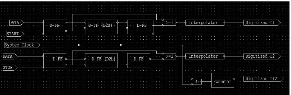
D. Interpolation Based TDC
The digitized time interval is measured in three parts as shown in fig.4. The main part T12 is synchronous with reference
to system clock and digitized by counter clock pulses. With a counter and a 100MHz clock a single shot measurement resolution of 10ns is achieved. The measurement time increased. So, to improve the single shot resolution with the interpolators.
The time interval T1, T2 and T12 are shown in fig.4. At the rising edge of start (stop) pulse, the erroneous measurement is possible due to excess delay line in flip-flop D2a (D2b). To reduce this possibility, T1 (T2) is not taken from the first but second clock pulse following the start (stop). Thus if flip-flop settle in less than one clock period the measurement is not affected[4].
Fig 4: Block diagram and Operating Principle of TDC
Fig 5: Principle of Interpolator
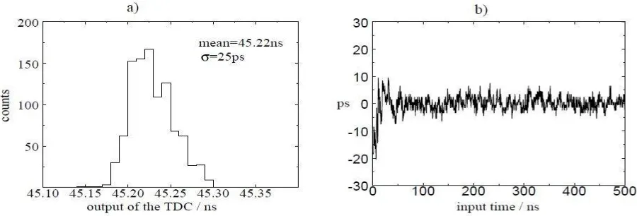
The single Shot resolution of TDC was measured by value for constant time interval. One pulse give the START input of TDC and other pulse delay to coaxial cable and then fed into STOP input. Thus, approximately jitter free input time interval was created. Fifteen different time interval measured from 5ns to 140ns. The measured worst case
value was 25ps as shown in fig. 6(a).
COMPARISON OF VARIOUS DESIGN METHODS OF TDC
Delay line TDC Pulse Shrinking TDC Interpolation Based TDC
Ref. [2] [3] [1]
Technology[nm] 90 800 90
Resolution[ps] 20 37.5 4.7
Single shot Precision - 0.7 LSB 0.7 LSB
Normalized Power 157 - 14
Area [mm2] 0.01 0.105 0.02
III. CONCLUSION
As the Scaling of time resolution is preferable to voltage resolution, the need for high resolution TDCs will absolutely increase. However high precision TDC are not simply digital circuits which can be synthesis automatically. So, the design is more preferable in full custom i.e. analog waveforms, signal synchronization, etc., and keeping analog criteria like noise, power supply and impedance matching. Also technology aspects variation in analog circuits.
REFERENCES
[1] Stephen Henzler,SiegmarKoeppe,Dominik Lorentz, Winpriedkamp, Ronald kuenemund, Doris Schmitt - landsiedel “A Local Passive Time Interpolation Concept for Variation-Tolerant High-Resolution ,” IEEE J. Solid-State Circuits, vol. 43, no. 7, pp. 1666–1676, July 2008.
[2] J.-P. Jansson, A. Mäntyniemi, and J. Kostamovaara, “A CMOS time-to-digital converter with better than 10 ps single-shot-precision,” IEEE J. Solid-State Circuits, vol. 41, no. 6, pp. 1286–1296, Jun. 2006.
[3] Pokichen,Shen-luanliu and Jingsgown “A Low Power High accuracy CMOS time to Digital Converter” IEEE symposium on circuits and systems,pp.281-284 , June 1997
[4] E. Raisanen-Ruotsalainen, T. Rahkonen, and J. Kostamovaara, “A high resolution time-to-digital converter based on time-to-voltage interpolation,” in Proc. 23rd European Solid-State Circuits Conf. (ESSCIRC), 1997, pp. 332–335.
[5] Timo E .Rahkomer, juha T. kostamovaara “The Use of Stabilized CMOS Delay Lines for the Digitization of Short Time,” IEEE J. Solid-State Circuits, vol. 28, no. 8, pp. 1666–1676, August 1993.