Optical loss suppression in long-wavelength semiconductor lasers at
elevated temperatures by high doping of the n-waveguide.
Boris S. Ryvkin
1,2, Eugene A.Avrutin
3, and Juha T.Kostamovaara
11 Dept of Electrical and Information Engineering, University of Oulu, Oulu, Finland 2A F Ioffe Physico-Technical Institute, St.Petersburg, Russia
3 Dept of Electronic Engineering, University of York, York, UK; corresponding author
Abstract: We show that strong n-doping of the n-waveguide layer substantially decreases the thermal carrier leakage from the active layer and the associated optical losses in III-V semiconductor lasers. The effect is particularly pronounced in devices operating at the wavelength region where the free hole absorption cross-section is much greater than that of free electrons. This is predicted to decrease the threshold current and improve the output efficiency of the lasers. An example of a bulk InGaAsP/ InP pulsed lasers is used to demonstrate that lasers with highly doped n-InGaAsP side of the waveguide can retain high output powers at ambient temperatures substantially above room temperature.
1. Introduction:
Long-wavelength (>~ 1.3 μm) semiconductor lasers find a host of applications, ranging from the traditional ones in optical communications to the more recent ones such as eye-safe optical radars. The latter application can also use devices operating at the shorter wavelength range of <~ 1 μm, though the longer-wavelength design has the advantage of being eye safe. It has to be noted that power characteristics of long-wavelength lasers tend to be substantially more modest than those of shorter-wavelength devices. This is due to a number of factors, the most important of which are the higher Auger recombination and the substantially larger cross-sections of intervalence band absorption (IVBA) by free holes, compared to the~1 μm devices. For that reason, the waveguides in high-power lasers tend to have a broad optical waveguide (optical confinement layer, OCL), in order to minimise the mode overlap with the p-cladding that contains equilibrium holes due to doping and is thus inherently lossy. The remaining holes, the source of IVBA, are then the nonequilibrium carriers. These come from the active layer and any carriers accumulated at high currents in the broad OCL itself. The accumulation of nonequilibrium carriers (both electrons and holes) in the OCL is due to the carrier transport through the OCL and the carrier generation by two-photon absorption at very high current densities, both of which result in inhomogeneous spatial carrier distribution, and the thermal escape of carriers from the active layer, which creates a spatially homogeneous “background”. The inhomogeneously distributed carriers are important at room temperature at very high injection current densities (pulsed operating regime) whereas the carriers generated by the
-thermal escape is likely to dominate at more modest currents and elevated temperatures (CW regime). The accumulation of spatially inhomogeneous carriers is strongly reduced by using a waveguide structure in which the active layer is positioned asymmetrically, near the p-emitter [1] [2], [3, 4] [5] [6]. In this case, the p-side of the OCL (the part between the active layer and the p-emitter, see inset to Figure 1), in which the inhomogeneous carriers accumulate more easily [7], is narrow, in extreme cases almost non-existent. In the previous paper [8], we have shown that the effect of the remaining inhomogeneously distributed carriers in the very wide n-OCL in the case of long-wavelength lasers, where the cross-section of IVBA by holes σh is much greater than the free electron absorption
cross-section σe, can be reduced further by strong n-doping of the n-part of the OCL, improving the laser
performance in the pulsed operating regime at room temperature (300K).
In the current paper, we shall show how the same method (high levels of n-doping of the n-OCL) can also reduce the spatially homogeneous density of electrons and holes in the (n-)OCL generated by thermal escape, and thus the corresponding optical losses, substantially improving the performance of the laser, particularly at elevated temperature (T>300K), but possibly at modest operating currents - a very different operating regime from that considered in [8], as will be explained in the next section.
2. The structure considered and calculations of the OCL hole density
Following the previous work, we analyse a strongly asymmetric laser structure, for either communications or radar applications. The basis of the analysis will be the calculation of the density of thermally activated OCL holes in the structure of interest. The “basis” structure considered here (shown in the Inset of Fig.1), intended for generation of 1.5 μm light at elevated temperatures, is very similar to that considered in the previous paper [8]. The structure involves a strongly asymmetric waveguide with the active layer located very close to the p-cladding. Such a design has been previously shown to enable lasing in a single transverse mode for any stripe width, with a narrow far field in the vertical direction [3] (for the structure of Figure 1, calculations give a far field of approximately 17° full width at half maximum) and to retain low optical losses up to high injection levels [7] [2, 4] as well as low electrical resistance [2], both contributing to highly efficient laser operation in either CW or pulsed regime [2]. Specifically in the case of CW operation, the structure has an additional advantage of having a lower thermal resistance (assuming p-side down mounting) than any design with the active laser location far from p-cladding. This additional advantage (particularly significant in InGaAsP materials with their relatively low thermal conductivity [9]) leads to decreased self-heating , contributing to power output and helping reduce the risk of Catastrophic Optical Degradation (the latter improvement is also aided by the relatively small confinement factor in such a structure). Still, in applications such as an automotive laser radar, operating at elevated temperatures, either through self-heating or because of the ambient conditions, remains probable [10]. Operating temperature limits are thus an important specification of a laser, so operating at elevated temperature will be considered here.
We note to begin with that very different physical mechanisms determine the losses in the laser in the elevated temperature case at moderate currents, compared to room-temperature, but very high current
-operation considered in [8]. The main absorption mechanism considered in [8], where the consideration was largely restricted to room temperature operation, was free carrier absorption by carriers accumulated in the OCL because of transport phenomena and distributed unevenly across the OCL depth. In contrast, the dominant absorption mechanism in the case of elevated temperature is that associated with carriers excited thermally from the AL into the OCL and distributed homogeneously across the OCL. Their density (negligible under the room-temperature conditions treated in [8]) must, and will, thus be accurately evaluated in the present study.
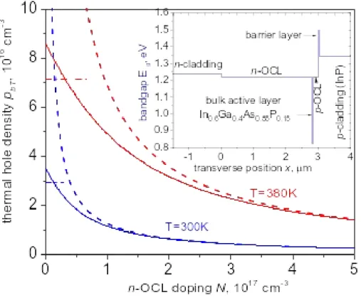
Figure 1..Thermally activated hole density in the OCL as function of the n-OCL doping at room and elevated temperatures. Solid: accurate calculation from Eq.(1) , dash – high-doping limit of Eq.(3) with
the carrier density dependence of bandgaps neglected , dash-dot – undoped material limit of Eq.(2). Inset: schematic of the structure used.
The structure still uses a bulk, relatively thick active layer (~ 500 A). We can assume quasineutrality both in the active layer and the surrounding waveguide layers. Together with the condition for continuity of the electron and hole quasi Fermi levels across the structure, this gives the condition for the thermally excited hole density pbT in the n-OCL in the form
(1a)
where
(1b)
and
(1c)
are the absolute quasi Fermi level separations in the n-OCL and the active layer respectively.
Furthermore, in (1), and are the electron and hole quasi Fermi levels in the n-OCL measured from the conduction band edge upwards and from the valence band edge downwards
respectively; and are the corresponding values in the active layer calculated
from the carrier density Na(i) in this layer (i being the injection current); is the density of
(ionised) donors in the n-OCL; and and are the OCL and active layer bandgaps, respectively, with temperature dependence and renormalisation due to carrier densities taken into account.
Generally speaking, Equation (1a) is a transcendental, if quite straightforward to solve, equation for pbT To our knowledge, this is the first reported use of the equation in this general form for
systematically investigating the thermal carrier excitation from the AC to the OCL. However Eq. (1) can be seen as a generalisation of two closed-form, analytical formulae found in the literature and constituting asymptotic solutions of (1) in the limiting cases of very weak and very strong doping.
Firstly, in the case of a weakly doped n-OCL (when < pbT), (1a) gives the formula [11]
(2)
where and stand for the equivalent electron and hole densities of states in the OCL.
Secondly, in the opposite case of a strongly doped n-OCL ( >>pbT), when the thermally
activated holes are the minority carriers in this layer, the activation formula similar to that originally used for minority electron escape into the p-cladding by [12] [13] and later adapted for minority hole escape from the AL into the n-OCL [8] is recovered from (1):
(3)
Both equations (2) and (3) are closed-form ones if the nonequilibrium carrier density dependences of the badgaps can be neglected. The difference between the expressions (2) and (3) reflects the different nature of carrier escape processes in the cases of undoped and strongly doped OCL. The
-formula (2) describes the bipolar escape of both electrons and holes into the undoped OCL. The expression (3) describes the case when holes (minority carriers in the n-OCL) are thermally activated from the active layer into the n-OCL; hence only the hole equivalent density of states features in the formula for this unipolar case.
An important feature of Eq. (1a), seen most clearly in the high-doping asymptotic form (3), is that the barrier seen by the holes is increased by substantial doping of the n-OCL which increases the
activation energy in (3), mainly due to , monotonically increasing with ND.
Figure 1 shows the calculated dependence of the n-OCL hole density on the n-OCL doping ND for
two values of temperature. Τhe limiting cases (2) and (3) are shown as dashed lines.
As can be expected, the increase in the hole activation energy with doping leads to the value of equation for pbT falling substantially with doping, similarly to the situation discussed in [12] [13] for
leakage of electrons from the active layer into the p-cladding.
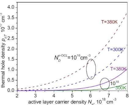
The value of the n-OCL hole density pbT is also dependent on the density of carriers Na in the active
layer, which determines the electron quasi Fermi level in (1). Figure 2 shows the dependences of pbT
on Na for two different temperatures, for the cases of undoped and strongly doped n-OCL.
Figure 2. Thermally activated hole density in the OCL as function of active layer carrier density at room and elevated temperatures.
As expected, the dependences are monotonically growing. Τhe value of pbT for the highly doped
n-OCL always stays below that for the (nearly) undoped case, the difference being particularly significant in the case of either high temperature and/or high values of Na.
3. Calculations of the optical characteristics of the laser.
The knowledge of the thermally escaped carrier densities makes it possible to calculate the internal absorption in the structure considered, which is determined mainly by free carrier absorption. It consists
of the built-in constant absorption by equilibrium carriers in the p-doped layers (p-cladding and p-side of the OCL), and absorption by the nonequlibrium carriers (mainly holes, since σh>>σe ), which
in turn includes absorption by the injected carriers in the active layer, the absorption
by the homogeneously distributed nonequilibrium carriers thermally activated
from the active layer into the n-OCL, and, lastly, the absorption by the inhomogeneously distributed nonequlibrium carriers supplied by the current flow and considered in [8]
(4)
Where, similarly to [8], the built-in optical absorption in the waveguide is calculated neglecting the small contribution of the n-cladding
(5)
(6)
(7)
As in the previous work [8], the parameters , , and are the waveguide mode overlaps with the corresponding layers (the contribution of the n-cladding is usually negligible). The
analytical expressions for the contribution in the case of low n-OCL doping can be found in [7]. In the case of arbitrary doping, the carrier distribution across the n-OCL is found as a
transcendental equation [14] and for calculating the absorption , simple numerical integration is required [8]. In both cases, the electron diffusion coefficient is the major parameter determining the carrier density distribution; the values we used are shown in Table 1.
Τhe major new features in equation (4) compared to the analysis conducted in the previous study [8]
are, firsrly, that the thermal contribution to the n-OCL loss, neglected in [8], is
-included in (4). In fact, it will be shown in the analysis below that it can be more important (at a high
temperature and in a non-optimised structure) than the non-thermal contribution
that was the focus of analysis in [8]. On the other hand, the direct and indirect
effects of two-photon absorption, which were considered for a similar structure but at extremely high
injection current densities in [8], do not need to be taken into account in the current study and are not
included in equation (4), because of the substantially lower values of intracavity power studied here
compared with those analysed in [8]. The second new feature in the analysis here, and hence in
equation (4), is that investigation of operation at elevated temperatures necessitates the inclusion of
temperature dependences of the parameters involved. In particular, the temperature dependence of
the free carrier absorption cross-sections was approximated as a linear dependence
the temperature dependences of other important parameters will be discussed later.
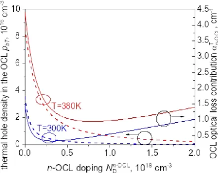
The calculated values of the n-OCL absorption are shown in Figure 3 as functions of the n-OCL doping (solid lines).
Figure 3. n-OCL doping dependence of the thermally activated hole density in the OCL (dashed) and the OCL optical loss (solid) for room and elevated temperatures.
It is clearly seen that at low doping levels, the value of is dominated by the thermally excited holes, whose density pbT is shown as dashed lines for reference. The absorption thus decays with
doping, as does pbT.. At high doping levels, however, the density of ionised donors, and hence of
equilibrium electrons, becomes so high that their absorption outweighs that of holes despite the fact that σh>>σe. The n-OCL absorption this slowly increases with ND at high doping layers. A broad minimum
-in is seen at ND of the order of 1017cm-3(the exact position of the minimum depends strongly on
the temperature, as seen in the figure)
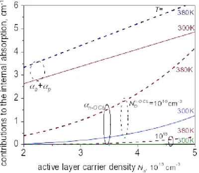
Figure 4 shows the major contributions to the internal absorption as functions of the active layer density that feature in Eq. (4).
Figure 4. Contributions to the optical absorption in the active structure of Figure 1 for the temperature of 300 K (solid curves) and 380 K (dashed curves) as function of carrier density
To analyse the threshold behaviour of a laser, we use the standard ABC model to describe the dependence of the carrier recombination rate Rrec on Na and thus relate the threshold value of the
carrier density to threshold current density jth.. At steady state, below the threshold of laser operation
(8)
The monomolecular recombination is assumed to be slow and so the temperature dependence of the recombination time nr~10-7 s can be ignored; the temperature dependence of the spontaneous
recombination coefficient B is described by a formula [15], and that of the Auger recombination coefficient C, as [16]
(9)
where the value of the thermal threshold (activation) energy was ≈ 60 meV [16]. The room-temperature values of B and C are given in Table 1.
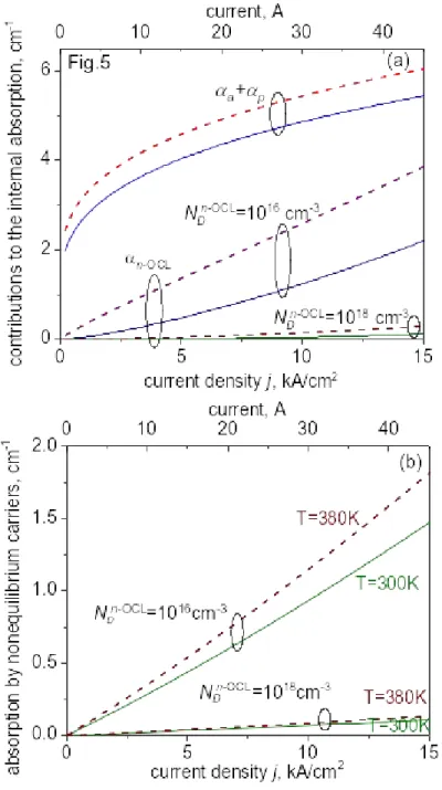
-Figure 5 shows the contributions to the internal absorption as functions of the injection current densities. Figure 5a presents the terms of Eq.(4) shown in Figure 4, with the carrier density recalculated into current density using Eq. (8) neglecting the stimulated emission. The figure this relates to an optical amplifier, or in the case of small current densities, a laser below threshold.
Figure 5b provides more detail on the absorption in the n-OCL by showing the current density dependence of absorption only by nonuniformly distributed nonequlibrium carriers in the (extremely wide) n-OCL [7]; the temperature dependence of the hole mobility and hence of the diffusion coefficient was calculated as described in [17]. These results are not affected by the threshold of laser operation and are thus valid at any injection current densities for both an SOA structure and a laser.
Figure 5. Contributions to the optical absorption in the active structure of Figure 1 for the temperature of 300 K (solid curves) and 380 K (dashed curves) as function of current density: (a) the major terms in Eq.(4); (b) the nonequilibrium carrier part of the loss in the n-OCL. The total values of current shown correspond to a stripe width of 100 µm and a resonator length of 3 mm.
-The characteristics of a practical device (the threshold current and the efficiency) are determined by the balance the internal losses calculated above and the gain provided by the active layer of the laser.
To implement the carrier density and temperature dependence of gain, we start with the linear relation
gm= σg(N-Ntr) with experimentally validated parameters for bulk InGaAsP at room temperature
(σg=3.1310-16 cm2, Ntr =6.51017 cm-3 [18]). This experimentally validated dependence was fitted, by
adjusting the scaling coefficient g0 at room temperature, to the simple semi-microscopic formula
obtained in the early paper by R.F.Kazarinov [19]:
(10)
where Nc and Nv are the effective densities of states in the conduction and valence band respectively.
The value of g0=2000 cm-1 was found to give a good agreement with room temperature data of [18]
within a broad range of carrier densities (1.5 – 6 ×1018 cm-3). The expression (10) was then used for
both room and elevated temperatures.
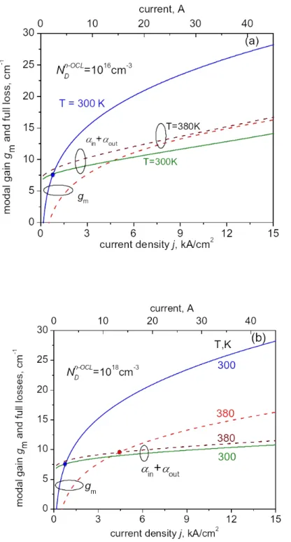
Figure 6 shows the carrier density dependences of the modal gain Гag (the active layer confinement
factor in our structure being Γa=0.0184) on injection current density for two temperatures. As in
Figure 5, stimulated emission is not taken into account, so the figure effectively shows unsaturated (small-signal) gain in an optical amplifier, or in the case of small current densities, gain in a laser below threshold. It is seen that in the low-doped structure (Figure 6a), the losses at elevated temperatures can rise so much with current that the gain cannot overcome them, meaning the absence of lasing at this temperature value (note that the value shown, 380 K, is very close to the critical temperature value (378 K) above which the laser ceases to switch on). This picture is in line with the well-established [20] [21] understanding of the role of OCL carrier accumulation in impeding, and ultimately preventing, lasing in quaternary III-V lasers at high temperatures. In contrast, in the structure with the highly doped n-OCL as proposed here, the (unsaturated) modal gain substantially exceeds the losses in a broad range of currents (above the intersection point shown as a bold dot on the curves), for both room and elevated temperature (Figure 6b), meaning successful laser operation at elevated temperatures. This will be confirmed more explicitly by the results shown in the following figures.
.
Figure 6. modal gain gm and total optical losses in the active structure of Figure 1 for the temperature
of 300 K (solid curves) and 380 K (dashed curves) in the case of low (a) and high (b) doping of the n-OCL. The output loss in both cases is αout= 5 cm-1. The total values of current shown correspond to a
stripe width of 100 µm and a resonator length of 3 mm.
The carrier density corresponding to the threshold of laser operation can be evaluated using the gain and losses as defined above substituted into the usual threshold condition
(11)
, where the threshold current density is evaluated from using Eq. (8).
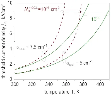
The resulting value of jth is shown in Figure 7 as function of temperature for high and low n-OCL
doping levels and two values of the output losses . It is seen that the increase in the threshold current with temperature, which is a well-known property of all laser diodes, is substantially less pronounced for the design with the high n-OCL doping.
Figure 7. Threshold of laser operation as function of the temperature for low-doped (dashed lines) and highly doped (solid lines) n-OCL designs.
We proceed then to calculate the light-current curves at different temperatures. Since in the design considered here, the cavity is short enough [6], and the AR facet reflectance is high enough [22] for the effect of the spatial hole burning to be rather weak, we use the usual lumped-model expression
(12)
Here is calculated from the current density j and the carrier density Na(j,T)in the active layer
using Eq. (4), the effective threshold current density is found from Na(j,T) using Eq. (8);
and the carrier density Na(j,T)> as function of current is evaluated self-consistently from the
modified version of (11) with the internal losses calculated at the current value j:
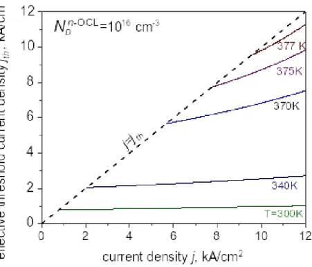
-Figure 8 shows schematically the increase in the effective threshold current density with current for the case of low doping (in the case of high doping, the effect is weak, so the corresponding lines are virtually horizontal at all temperatures within the range of currents studied). For low to modest temperature excess above the room temperature level (T = 300 and 340 K), the effective threshold increase is not strong either; however as seen from the figure, at high ambient temperature of 375-377 K
even a modest excess current above threshold leads to a situation of increasing almost at the same rate as j, which can be expected to result in extremely low powers. At higher temperatures, the laser does not switch on at all as shown in Figure 7, mainly due to the increased thermal excitation of
carriers and the associated optical losses .
Figure 8. Increase in the effective threshold current density with current for the low doping case of
= 1016 cm-3 The output loss is α
out= 5 cm-1.
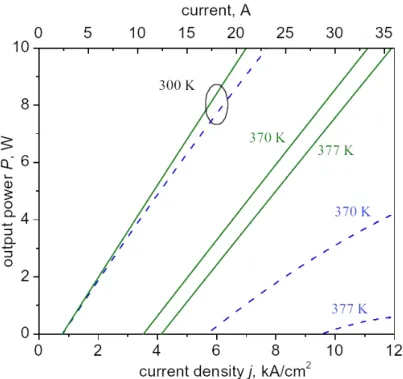
The calculated power output values are shown schematically in Figure 9. It is clearly seen that the high n-OCL doping is providing some improvement of the light-current characteristics at all operating temperatures. At room temperatures, however, the curves of Figure 8 are essentially the low-power sections of those presented in [8] and so the magnitude of the effect is modest. The advantage of the high n-OCL doping is more significant at elevated temperatures, when both the threshold and the output efficiency are substantially impoved by the reduced carrier accumulation in the OCL afforded by doping. At the highest temperatures shown (370-377 K), the laser with a low n-OCL doping level reaches saturation with extremely modest powers, in agreement with the results shown in Figure 8, whereas a similar design with a high n-OCL doping can yield substantial power output, albeit at an increased current compared to room temperature operation.
-Figure 9. Calculated light-current curves for a laser with = 1018 cm-3 (solid curves) and 1016
cm-3 (dashed curves) at room and elevated temperatures. The output loss in both cases is α
out= 5 cm-1.
The total values of current shown correspond to a stripe width of 100 µm and a resonator length of 3 mm, as in Figure 6.
It has to be noted that all calculations here have treated the temperature T as ambient temperature, which can be important, for example, in a Lidar for automotive applications, as mentioned above. However the results make it highly probable that the deterioration of the efficiency and power output of the laser due to the self-heating under true CW operation will also be reduced in the design proposed. Quantitative treatment of this effect requires knowledge of the thermal properties of the laser and its mount and is reserved for future work.
We note finally that the same strategy (high n-doping of the n-OCL) can also be expected to be beneficial in a stripe laser structure with a stongly asymmetric active layer position (near the p-cladding) but an otherwise symmetric waveguide, such as a slab-coupled optical waveguide laser (SCOWL; see e.g. [23]).
To conclude, we have presented a semi-analytical model of the effect of n-doping in the n-OCL on the output of a long-wavelength laser diode with a broad n-OCL at relatively modest injection/output power levels, but at an elevated temperature. It has been shown that the increase in the effective barrier for
-thermal excitation of holes from the active layer into the (n-)OCL due to doping leads to a significant reduction in the thermal accumulation of highly absorbing holes in the n-OCL, improving both the
slope efficiency and the threshold current density of the laser, and thus leading to a substantial improvement in the power output.
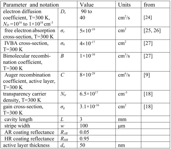
-Table 1. The main parameters in the calculations.
Parameter and notation
Value
Units
from
electron diffusion
coefficient,
T=300 K,
N
D=10
16to 1×10
18cm
-3D
e90 to
40
cm
2/s
[24]free electron
absorption
cross-section, T=300 K
σ
e5
10
-19cm
2[25, 26]
IVBA cross-section,
T=300 K
σ
h4
10
-17cm
2[27]
Bimolecular
recombi-nation coefficient,
T=300 K
B
1×10
-10cm
3/s
[27]
Auger recombination
coefficient, active layer,
T=300 K
C
8×10
-29cm
6/s
[9]
transparency carrier
density, T=300 K
N
tr6.5×10
17cm
-3[18]
gain cross-section,
T=300 K
σ
g3.1×10
-16cm
2[18]
cavity length
L
3
mm
stripe width
w
100
μm
AR coating reflectance
R
AR0.05
HR coating reflectance
R
HR0.95
active layer thickness
d
a50
nm
-References
[1] B. Ryvkin, E. A. Avrutin, and J. T. Kostamovaara, "Asymmetric-Waveguide Laser Diode for High-Power Optical Pulse Generation by Gain Switching," Journal of Lightwave Technology,
vol. 27, no. 12, pp. 2125-2131, Jun 2009.
[2] P. Crump et al., "Efficient High-Power Laser Diodes," IEEE Journal of Selected Topics in Quantum Electronics, vol. 19, no. 4, Jul-Aug 2013, Art. no. 1501211.
[3] B. Lanz, B. S. Ryvkin, E. A. Avrutin, and J. T. Kostamovaara, "Performance improvement by a saturable absorber in gain-switched asymmetric-waveguide laser diodes," Optics Express,
vol. 21, no. 24, pp. 29780-29791, Dec 2013.
[4] K. H. Hasler et al., "Comparative theoretical and experimental studies of two designs of high-power diode lasers," Semiconductor Science and Technology, vol. 29, no. 4, p. 045010, Apr 2014, Art. no. 045010.
[5] Y. Kaifuchi, Y. Yamagata, R. Nogawa, R. Morohashi, Y. Yamada, and M. Yamaguchi, "Ultimate high power operation of 9xx-nm single emitter broad stripe laser diodes," in High-Power Diode Laser Technology Xv, vol. 10086, M. S. Zediker, Ed. (Proceedings of SPIE, 2017.
[6] T. Kaul, G. Erbert, A. Maassdorf, S. Knigge, and P. Crump, "Suppressed power saturation due to optimized optical confinement in 9xx nm high-power diode lasers that use extreme double asymmetric vertical designs," Semiconductor Science and Technology, Article vol. 33, no. 3, p. 9, Mar 2018, Art. no. 035005.
[7] B. S. Ryvkin and E. A. Avrutin, "Asymmetric, nonbroadened large optical cavity waveguide structures for high-power long-wavelength semiconductor lasers," Journal of Applied Physics, vol. 97, no. 12, p. 123103, Jun 2005, Art. no. 123103.
[8] B. S. Ryvkin, E. A. Avrutin, and J. T. Kostamovaara, "Strong doping of the n-optical confinement layer for increasing output power of high-power pulsed laser diodes in the eye safe wavelength range," Semiconductor Science and Technology, vol. 32, no. 12, Dec 2017, Art. no. 125008.
[9] L. A. Coldren, S. W. Corzine, and M. K. Mashanovitch, Diode Lasers and Photonic Integrated Circuits, 2nd ed. NY: Wiley, 2012.
[10] G. Refai-Ahmed, H. Do, A. Raghupathy, R. Kadam, J. Gillis, and Ieee, Thermal Design of Monocular Vision System used in Automotive Application (2017 18th International Conference on Thermal, Mechanical and Multi-Physics Simulation and Experiments in Microelectronics and Microsystems). New York: Ieee, 2017.
[11] G. W. Taylor and P. R. Claisse, "Transport solitions for the SCH Quantum Well laser diode,"
IEEE Journal of Quantum Electronics, Article vol. 31, no. 12, pp. 2133-2141, Dec 1995.
[12] G. P. Agrawal and N. K. Dutta, Long-wavelength semiconductor lasers. New York: Van Nostrand Reinhold, 1986.
[13] P. M. Smowton et al., "The effect of cladding layer thickness on large optical cavity 650-nm lasers," IEEE Journal of Quantum Electronics, vol. 38, no. 3, pp. 285-290, Mar 2002, Art. no. Pii s0018-9197(02)01752-9.
[14] E. A. Avrutin and B. S. Ryvkin, "Dember type voltage and nonlinear series resistance of the optical confinement layer of a high-power diode laser," Journal of Applied Physics, vol. 113, no. 11, Mar 2013, Art. no. 113108.
[15] B. L. Gelmont and G. G. Zegrya, "Temperature dependence of the threshold current density of an injection heterolaser," Soviet Physics Semiconductors-Ussr, vol. 25, no. 11, pp. 1216-1218, Nov 1991.
[16] V. N. Abakumov, V. I. Perel, and I. N. Yassievich, Nonradiative Recombination in Semiconductors. North Holland.
[17] B. L. Gelmont, M. Shur, and M. Stroscio, "Polar optical-phonon scattering in 3-dimesional and 2-dimensional electron gases," Journal of Applied Physics, vol. 77, no. 2, pp. 657-660, Jan 1995.
[18] J. Leuthold, M. Mayer, J. Eckner, G. Guekos, H. Melchior, and C. Zellweger, "Material gain of bulk 1.55 mu m InGaAsP/InP semiconductor optical amplifiers approximated by a polynomial model," Journal of Applied Physics, vol. 87, no. 1, pp. 618-620, Jan 2000.
-[19] R. F. Kazarinov, "Maximum reduction of threshold current density in double heterostructio injeciton lasers," Soviet Physics Semiconductors-USSR, vol. 7, no. 4, pp. 525-531, 1973. [20] H. Temkin et al., "High-temperature characteristics of InGaAsP/InP laser structures," Applied
Physics Letters, vol. 62, no. 19, pp. 2402-2404, May 1993.
[21] S. Seki, H. Oohasi, H. Sugiura, T. Hirono, and K. Yokoyama, "Dominant mechanism for limiting the maximum operating temperature of InP-based multiple-quantum-well lasers," Journal of Applied Physics, vol. 79, no. 5, pp. 2192-2197, Mar 1996.
[22] F. Rinner, J. Rogg, P. Friedmann, M. Mikulla, G. Weimann, and R. Poprawe, "Longitudinal carrier density measurement of high power broad area laser diodes," Applied Physics Letters,
vol. 80, no. 1, pp. 19-21, Jan 2002.
[23] J. J. Plant, P. W. Juodawlkis, R. K. Huang, J. P. Donnelly, L. J. Missaggia, and K. G. Ray, "1.5-mu m InGaAsP-InP slab-coupled optical waveguide lasers," IEEE Photonics Technology Letters,
Article vol. 17, no. 4, pp. 735-737, Apr 2005.
[24] M. Levinshtein, S. Rumyantsev, and M. Shur, Eds. Semiconductor Parameters: Ternary And Quaternary III-V Compounds Singapore: World Scientific, 1996.
[25] S. Krishnamurthy, Z. G. Yu, L. P. Gonzalez, and S. Guha, "Temperature- and wavelength-dependent two-photon and free-carrier absorption in GaAs, InP, GaInAs, and InAsP," Journal of Applied Physics, vol. 109, no. 3, Feb 2011, Art. no. 033102.
[26] G. Kyritsis and N. Zakhleniuk, "Performance of Widely Tunable MultiQuantum-Well and Bulk Laser Diodes and the Main Limiting Factors," IEEE Journal of Quantum Electronics, vol. 53, no. 3, 2017, Art. no. 2500216.
[27] J. Piprek, Semiconductor Optoelectronic Devices: Introduction to Physics and Simulation. San Diego, CA: Academic Press, 2003.