Ultra Sharp Photonic Bends: A Review
Mohit Chawla
1, Jyoti Kedia
2P.G.Student, Dept. of Electronics and Communication Engineering, PEC University of Technology, Chandigarh, India1
Assistant Professor, Dept. of Electronics and Communication Engineering, PEC University of Technology,
Chandigarh, India2
ABSTRACT: The information carrying capacity of Electronics circuits is of the order of GHz whereas the optical waveguides on integrated circuits can carry the information using light (Optoelectronic) i.e. using a frequency of the order of THz. Thus optical waveguides can be used to carry the information in VLSI circuit e.g. Microprocessors at the speed of light. The optical waveguide empowers not only an enormous bandwidth increase i.e. in the range of multiple terabits per second, but causes a decrease in power consumption, reduced immunity to temperature variations, immunity to electromagnetic noise interference, etc. Hence the design and investigation of high transmission and low bending loss by photonic crystal waveguide has been a subject of strong interest in the past decade. In this paper different technique used for designing optical waveguide bends, the different bending angles along with their transmission efficiency through the bend at various frequencies have been discussed and compared. From the tabular comparison it can be observed that the material is to be chosen with a high refractive index contrast and by adjusting the position, size, structure and refractive index of the holes at the bend to maximize the overall transmission efficiency.
KEYWORDS: Photonic Integrated Circuit, Photonic Crystal waveguide, Bending radius, Transmission efficiency, Bandwidth.
I. PHOTONICS INTRODUCTION
ISSN(Online): 2319-8753 ISSN (Print): 2347-6710
I
nternational
J
ournal of
I
nnovative
R
esearch in
S
cience,
E
ngineering and
T
echnology
(A High Impact Factor, Monthly Peer Reviewed Journal)
Vol. 5, Issue 1, Januray 2016
paper the concentration is basically on the bending losses incur by the waveguides at different bending angles. The different techniques and materials for a waveguide which are used to enhance the transmission efficiency at different frequencies are also studied and depicted in a tabular form.
II. SILICON PHOTONICS
Silicon has been for many years the base material for microelectronic devices. Silicon photonics is the study and application of photonic systems which use silicon for optical switching and optical waveguide for data transfer. Silicon photonic devices are considered because Si is abundantly available and devices can be made using existing semiconductor fabrication techniques. An additional advantage for using Si is the high refractive index which is helpful in attaining high refractive index contrast for the confinement of light within the waveguide as shown in Fig.1 so to utilize the advantages of both hybrid devices are used.
Fig.1 Refractive indexes of materials employed to build optical waveguides
III.BENDING LOSSES
The different types of losses in an optical waveguide can be absorption loss, coupling loss, waveguide loss, bending loss and insertion loss. All the losses mentioned can be minimized. Absorption loss can be minimized by changing the material used for the waveguide, coupling loss by increasing the cross-section of the waveguide, waveguide loss by taking care at the time of manufacturing to reduce the material imperfection and insertion loss by using the material of some other type. But the Bending Loss cannot be much reduced so it contributes a large percent of loss. That’s the reason why bending losses need to be studied.
To establish a connection between two components (i.e. through routing) in a Photonic Integrated Circuit (PIC) there are two possibilities:
One can imagine a series of straight waveguide joined together at the junction abruptly but there would be losses at each abrupt junction.
Second method is to introduce a curved waveguide between two straight waveguides which allows a gradual transition from one direction to other and reduce the losses. Along the bend in order to maintain phase relationship across the mode, the light at outer arc of the bend moves quicker as compared to the one travelling along the inner arc of the bend. But the material within the circular waveguide is same so light cannot travel at two different velocities in same refractive index material.
This is the main reason for losses at the bend [3].
IV.OPTICAL WAVEGUIDES
A waveguide used at optical frequencies is an optical waveguide. It can be developed through two most profound techniques, which are:
1. Rectangular Dielectric Waveguide
Fig.2 Types of Rectangular Waveguides
A buried channel waveguide (also known as overlayer waveguide) is formed with a high-index wave guiding core buried in a low-index surrounding medium.
A strip waveguide has a structure that looks like a strip/wire/ridge waveguide. Strip on top of the planar structure has a high refractive index and is actually the wave guiding core. A strip waveguide has a strong optical confinement because it is surrounded on three sides by low-index air (or cladding material).
A rib waveguide has it’s structure similar to that of a wire or strip or ridge waveguide, but the strip has the same index as the high index planar layer beneath it and is part of the wave guiding core [4].
Of these three waveguides, Rib waveguide has larger cross-section as compared to the other two waveguides so it provides high coupling efficiency but on the contrary it requires the larger area hence the chip density decreases so overall performance decreases. This is the main reason why rib waveguide is not used and other two waveguides are mainly taken into consideration.
In the recent past, various methods were proposed by different authors to determine the bending loss. The authors present a low loss, hybrid silicon waveguide consisting of a straight rib section and compact photonic wire bends. The rib and wire waveguides are both single mode and are connected through a short double-etched linear taper section. Due to the introduction of spline much improvement in bending losses comes forth for first 10o spline angles and bending radius less than 3.5 µm [5]. Another authors determined the bending loss in hybrid (Rib/wire) waveguide where bend rib section and straight wire section is used. In this paper transmission efficiency is increased to 90% but the bending radius also increases [6]. All the observations from different papers are depicted in the tabular form in Table.1
2. Photonic Crystal Waveguide
A major drawback of conventional dielectric waveguides is that their bending radii are limited to several millimeters due to the degradation of total internal reflection. Since the guiding of light in a PC defect waveguides is not given through total internal reflection but the photonic bandgap (PBG) effect they can provide bending within the sub-wavelength range.
Photonic crystals are periodic structures with large refractive index contrast and the lattice prohibits the propagation of certain EM waves due to the gaps in the energy band structure of the crystal, i.e. the electrons are forbidden to propagate with certain energies in certain directions. If the potential is strong enough, the gap can extend for all directions in some energies (or frequencies), resulting in a complete band gap, called Photonic Band Gap (PBG) or Electromagnetic Band Gap (EBG). This is much similar to the semiconductors theory where the valence band and the conduction band are separated by the band gap.
One can consider it as an array of elements with high dielectric constant immerses a low dielectric constant media or in other words the holes with low dielectric constant in a high dielectric constant media.
ISSN(Online): 2319-8753 ISSN (Print): 2347-6710
I
nternational
J
ournal of
I
nnovative
R
esearch in
S
cience,
E
ngineering and
T
echnology
(A High Impact Factor, Monthly Peer Reviewed Journal)
Vol. 5, Issue 1, Januray 2016
Different authors stressed on various materials to decimate the bending radius and thereby the bending loss at distinct bending angles to enhance the transmission efficiency shown in Table 1.
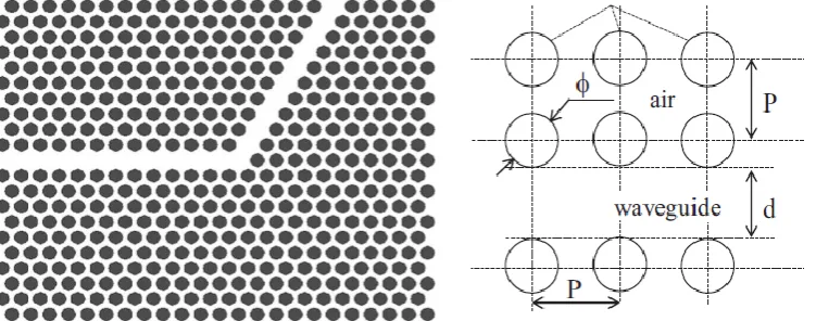
Fig.3Schematic view of the simple 2-D photonic crystal Fig.4 Top view of fundamental square lattice and
waveguide bends photonic crystal waveguide
Schematic view of a Square lattice 2D photonic crystal waveguide with 60o bend is shown in Fig.3 [8]. The same figure in magnified form is shown in Fig.4 [9] in which we can see holes or rods in a cluster forms a photonic crystal. These rods can be of different materials which are contained in a substrate. The difference between two rods is P i.e. lattice constant. Generally the transmission efficiency for a photonic crystal waveguide is 90% for entire C band. To enhance the efficiency various steps can be taken like choosing a proper guided mode in the bend waveguide, which has a mode pattern similar to the guided mode in the straight waveguide. Then, alter the band structure of the waveguide bend by adjusting the size and position of the air holes near the bend corner in order to have a wider frequency region. In this region, the wave number of the mode in the bend waveguide matches that of the straight waveguide. The Optimized waveguide is shown in Fig.5 [8].
Fig.5 Schematic view of the optimized 2-D Photonic Crystal waveguide bend
By adjusting the size and the position of rods/holes at the bend corner affects the transmission efficiency.
The positions of holes need to be changed such that the wave number of the mode in the bend waveguide matches that of the straight waveguide. In other sense the field intensity of both the straight and the bend waveguide should overlap hence the difference between their peaks to be equal to the shift in the lattice points [10].
Fig.6 Layout of the drop hole used for structure tuning in the Fig.7 Schematic drawing of 180° bend waveguide 180° waveguide bends
Normalized transmission as high as 99.4% is achieved at 1550 nm optical wavelength and it is greater than 94% for nearly the entire optical C-band. Such a high transmission efficiency can be attained for large frequency band but drop holes is rarely used because it is difficult to fabricate. Hence the structure of the rods at the bend must be an easy one to fabricate.
Different losses are experienced by varying the material of rods. Two distinct photonic crystal structure consisting of dielectric (i.e. ceramic) and metallic (i.e. aluminium) rods are compared with respective straight waveguides and the efficiency is computed [9]. This shows that the transmission efficiency varies with the material of the rods.
Implicitly single line defect is taken to make a waveguide but with the increase in the number of lines of defect the overall efficiency also increases. The improvement in the efficiency is greater if the number of holes displaced at the bend corner increases [12].
The Photonic crystal waveguide because of its large area cannot be used as both straight and bend waveguide so it can only be used at the bends and for the straight waveguides there is need for some other waveguide As nano-wire waveguide offers less propagation loss for straight waveguides so a hybrid waveguide consisting of bend photonic crystal waveguide and straight nano-wire waveguide designed with low index trenches is presented in the Fig.8 [13].
ISSN(Online): 2319-8753 ISSN (Print): 2347-6710
I
nternational
J
ournal of
I
nnovative
R
esearch in
S
cience,
E
ngineering and
T
echnology
(A High Impact Factor, Monthly Peer Reviewed Journal)
Vol. 5, Issue 1, Januray 2016
TABLE1.COMPARATIVE ANALYSIS OF DIFFERENT TECHNIQUES
Material Technique
Bending Radius
(µm)
Angle Bending Loss
(dB/90o)
Efficiency (%) SOI Hybrid (Rib/Wire) waveguide [5]
Double etched taper (Spline)
5 90
o
α=20o 0.0273
_
3 90
o
α=10o 0.037
SOI Hybrid [6]
Asymmetric Rib structure with and without outer
slab region
200
90o
1.15 90%
800 4.7 60%
SOS (Wire) waveguide [14] _ 1700 90o 10.34 _
2550 2
4500 0
SOI (Wire) waveguide
[14]
10
90o
1.233
20 0.072
30 0.004
Silicon Oxynitride
(SiON) [15]
Wire waveguide 2 90o 0.086 _
Si based [16]
Photonic Crystal
Waveguide _ 90
o _ 90.9%
GaAs substrate & Al0.9Ga0.1As
(vertical confinement)
[17]
Photonic Crystal Slab 1.5 60o _ 90%
SOI Hybrid (Photonic crystal
and nano-wire) waveguide
[13]
Hybrid waveguide with
Low Index Trenches _ 120
V. CONCLUSION
This review paper is giving a precise knowledge of optical waveguides bends. Dielectric Waveguide experiences large losses at the bend whereas the Photonic Crystal Waveguide incurs less loss at the bend and is also a suitable choice to get sharper bendsso chip density increases.The material of the waveguide is to be chosen with a high refractive index contrast (preferably Si as abundantly available) and by adjusting the position, size, structure and
SOI [18]
Cubic Photonic Crystal (Adding 3 holes at
corners)
_ 90o _ 96.8%
Si substrate [11]
Photonic crystal slab with
3 Drop Holes 1 180
o _
99.4%
> 94% for entire C band
Ga(Al)As [8]
Photonic crystal (Mode pattern and wave
no. match)
_ 60o _ > 90% for entire C
band InGaAsP (guiding layer) n+ InP (substrate) [19] Photonic crystal
waveguide _ 60
o _ 96.8%
GaInAsP (guiding layer) InP (substrate) [12] Photonic crystal (More than 1 line defect
+ Displacing 3 holes)
_ Double 60o _ 99%
Si substrate [9] Photonic crystal Dielectric (Ceramic) & Metallic (Aluminium) rods _ Double 90o Crankshaped bend _ 89% 65% Si substrate [10] Photonic crystal overlapping fields of
straight and bend waveguide
_
60o
_
72.7 - 87.5%
ISSN(Online): 2319-8753 ISSN (Print): 2347-6710
I
nternational
J
ournal of
I
nnovative
R
esearch in
S
cience,
E
ngineering and
T
echnology
(A High Impact Factor, Monthly Peer Reviewed Journal)
Vol. 5, Issue 1, Januray 2016
crystal waveguide the transmission efficiency of 94% (for entire C band) and approximately 99% for particular frequencies can be obtained. The Photonic crystal waveguide cannot be used as both straight and bend waveguide because of its large area so it can only be used at the bends and for the straight waveguides there is need of some other waveguide to get a Hybrid waveguide. Finally, it can be concluded that a serious research work in the field of hybrid optical waveguide is going on to enhance the efficiency of transmission, bandwidth with low bending loss at different bending angles for different waveguide materials.
REFERENCES
[1] Nikolaos Bamiedakis, Richard V. Penty, “Compact Multimode Polymer Waveguide Bends for Board-Level Optical Interconnects “27-28 December, 2013, BIAM Foundation.
[2] Michele Petracca, Keren Bergman, Luca P. Carloni,” Photonic Networks-on-Chip: Opportunities and Challenges”, J. Sel. Topics Quantum Electron., 978-1-4244-1684-4/08,pp.2789-2792, 2008 IEEE.
[3] L. Pavesi, G. Guillot ”Optical Interconnects –The Silicon Approach “Book published by Springer in 2006.
[4] Isha Gulati,” Design And Comparison Of Waveguides For Photonic Integrated Circuits ”M.E Thesis, PEC University of Technology.
[5] W. Bogaerts and S. K. Selvaraja,” Compact Single-Mode Silicon Hybrid Rib/Strip Waveguide with Adiabatic Bends” Photonics Journal, pp. 422-432, 2011_IEEE.
[6] Rupesh Kumar Navalakhe, Nandita Dasgupta and Bijoy Krishna Das, “Design of Low-Loss Compact 90° Bend Optical Waveguide for Photonic Circuit Applications in SOI Platform”, IEEE Region 10 Colloquium and the Third ICIIS, Kharagpur, pp. 1-5,IEEE 2008.
[7] T. P. Pasetto, A.S.B. Sombra, V.F.Rodríguez Esquerre and H.E. Hernández Figueroa “Pedagogical Microwave Design of Photonic Crystal Waveguides”, pp. 932-936, 2011 IEEE.
[8] Gang Ren, Wanhua Zheng, Yejin Zhang, Ke Wang, Xiaoyu Du, Mingxin Xing and Lianghui Chen, “ Mode Analysis and Design of a Low-Loss Photonic Crystal 60o Waveguide Bend", Journal Of Lightwave Technology, Vol. 26, No. 14, pp. 2215-2218, 2008 IEEE.
[9] Hiroshi Maeda, Kiyotoshi Yasumoto, “Bending Loss in Two Dimensional Photonic Crystal Waveguide”, 9th International Conference on Complex, Intelligent, and Software Intensive Systems, pp. 24-27, 2015 IEEE.
[10] Ming-Feng Lu, Yu-Lin Yang, and Yang-Tung Huang, “Numerical Study of Transmission Improvement in a Photonic Crystal Waveguide Bend by Mode-Matching Technique”, Photonics Technology Letters, Vol. 20, No. 24,pp. 2114-2116, 2008 IEEE.
[11] Din Chai Tee, Yu Gang Shee, Nizam Tamchek, and Faisal Rafiq Mahamd Adikan, “Structure Tuned, High Transmission 180º Waveguide Bend in 2-D Planar Photonic Crystal”, PHOTONICS TECHNOLOGY LETTERS, VOL. 25, No. 15, pp. 1443-1446, 2013 IEEE.
[12] A.Talneau , L.Le Gouezigou, N.Bouadma, “Very efficient ultra-short bends on 2D Photonic-crystal waveguide on InP substrate”, Proc. 27th Eur. Conf. on Opt. Comm., pp. 588-589, 2001.
[13] S. H. Tao, M. B. Yu, Q. Fang, J. F. Song, R. Yang, G. Q. Lo, and D. L. Kwong, “High Transmission Photonic Crystal Line-defect Bend with Double Low-index Trenches”, pp. 154-156, 2007 IEEE.
[14] Imran Khan and Md. Mostafizur Rahman, “Bending Loss Analysis of Optical Waveguide for SOI & SOS Material System towards Photonic Integration”BIAM Foundation 27-28 December, pp. 1-8, 2013.
[15] Yurii A. Vlasov and Sharee J. McNab, “Losses in single-mode silicon-on-insulator strip waveguides and bends”, Optics Express, Vol. 12, No. 8, pp. 1622-1631, 2014 Optical Society of America.
[16] A. Vukovic, P. Sewell, T. M. Benson, “Optimised Compact 90o Optical Waveguide Bend”, 12th International Conference in Electromagnetic
Theory, pp. 130-132, 2008 IEEE.
[17] E. K.C. Chow, S.Y. Lin, S.G. Johnson, J.D. Joannopoulos, J. Bur and P.R. Villeneuve,“Demonstration of high waveguide bending efficiency (>90%) in a photonic-crystal slab at 1.5μm wavelengths” Physics and Simulation of Optoelectronic Devices IXProceedings of SPIE, Vol. 4283, pp. 453-461, 2001.
[18] Yih-Bin Lin, Jia-Sheng Lin, Rei-Shin Chen, and Cheng-Ru Li, “Design of High Transmission Broadband 90-Degree Bend by Reducing Field Mismatch at Corner for Two Dimensional Cubic Photonic Crystals”, 2008 Optical Society Of America.
[19] K. Rauscher, D. Erni, J. Smajic, Ch. Hafner, “Improved Transmission for 60° Photonic Crystal Waveguide Bends”, Electromagnetic Research Symposium, pp. 25-28, 2004 Pisa, Italy.
[20] D. C. Tee, N. Tamchek, M. H. Abu Bakar, F. R. Mahamd Adikan, “High-Transmission-Efficiency 120o Photonic Crystal Waveguide Bend by