Structural TEM study of nonpolar
a
-plane gallium nitride grown on
„
112
¯
0
…
4
H
-SiC
by organometallic vapor phase epitaxy
Dmitri N. Zakharov*and Zuzanna Liliental-Weber
Materials Sciences Division, Lawrence Berkeley National Laboratory, 1 Cyclotron Road, Mail Stop 62-203, Berkeley, California 94720-8253, USA
Brian Wagner, Zachary J. Reitmeier, Edward A. Preble, and Robert F. Davis Materials Science and Engineering Department, North Carolina State University, 2401 Stinson Drive,
Raleigh, North Carolina 27695-7907, USA
共Received 21 June 2004; revised manuscript received 27 April 2005; published 30 June 2005兲
Conventional and high-resolution electron microscopy have been applied for studying lattice defects in nonpolar a-plane GaN grown on a 4H-SiC substrate with an AlN buffer layer. Samples in plan-view and cross-sectional configurations have been investigated. Basal and prismatic stacking faults together with Frank and Shockley partial dislocations were found to be the main defects in the GaN layers. High-resolution electron microscopy in combination with image simulation supported Drum’s model for the prismatic stacking faults. The density of basal stacking faults was measured to be⬃1.6⫻106cm−1. The densities of partial dislocations
terminating I1and I2 types of intrinsic basal stacking faults were⬃4.0⫻1010cm−2and ⬃0.4⫻1010cm−2,
respectively. The energy of the I2 stacking fault in GaN was estimated to be共40± 4兲erg/ cm2based on the
separation of Shockley partial dislocations.
DOI: 10.1103/PhysRevB.71.235334 PACS number共s兲: 68.55.Jk, 61.72.Nn, 68.37.Lp
I. INTRODUCTION
Wurtzite III-nitride heterostructures have been shown to be promising materials for laser and light-emitting diodes. They are usually grown on共0001兲 Al2O3, 6H-SiC, or free-standing GaN substrates.1–3In devices based on such mate-rials, active GaN-based heterostructural epilayers have the polarcaxis of the hexagonal structure perpendicular to the sample surface and to the interfaces of the active layers. Since Ga and N atoms are arranged on top of each other along the polar关0001兴 crystallographic direction, this leads to nonzero spontaneous polarization. In addition, in hetero-structures, stress applied along the same axis can also give rise to piezoelectric polarization. The total polarization, which is the sum of spontaneous and piezoelectric polariza-tions, is aligned along the 关0001兴 direction of the wurtzite III-nitride heterostructures. The change in the total polariza-tion across the heterolayers results in high interface charge densities and spatial separation of the electron and hole wave functions, redshifting the photoluminescence peak and de-creasing the peak intensity.4–6One of the possible solutions to eliminate these undesirable effects is to grow GaN-based epilayers in nonpolar orientations. Recently, nonpolar m-plane and a-plane GaN/ AlGaN multiple quantum well structures have been grown on 共100兲 ␥-LiAlO2 and 共11¯02兲 r-plane Al2O3 substrates, respectively. These layers show a lack of redshift and an improved photoluminescence intensity.7–10Investigations of similar layers by transmission electron microscopy revealed high densities of basal stacking faults and threading dislocations.11,12
共112¯0兲4H-SiC is an alternative substrate suitable for a-plane GaN-based layer growth. In this paper growth of a-plane GaN layers on the共112¯0兲surface of a 4H-SiC
sub-strate by organometallic vapor phase epitaxy is reported. Be-cause the optoelectronic properties of the layers depend on structural quality, systematic studies of the layers grown in the nonpolar direction were performed by conventional and high-resolution electron microscopy.
II. DEFECTS IN THE WURTZITE STRUCTURE
GaN exists in two different polytypes, namely, wurtzite and sphalerite. The wurtzite structure consists of two hex-agonal close-packed sublattices共Ga and N兲shifted by 0.377c along 关0001兴. In both sublattices 共0002兲 planes are close packed. Stacking these basal 共0002兲 planes in the …A␣BA␣BA␣B…sequence forms the wurtzite struc-ture, in which the atoms are tetrahedrally coordinated. Here capital letters correspond to Ga layers and the Greek letters to N layers. For simplicity the GaN molecule can be taken as a stacking unit. In this case the Greek letters can be omitted. Thus the hexagonal stacking sequence will further be re-ferred to as …ABABAB…, where capital letters represent Ga-N atomic bilayers. In the above notation the sphalerite structure can be represented as an…ABCABCABC… stack-ing sequence along the关111兴direction.
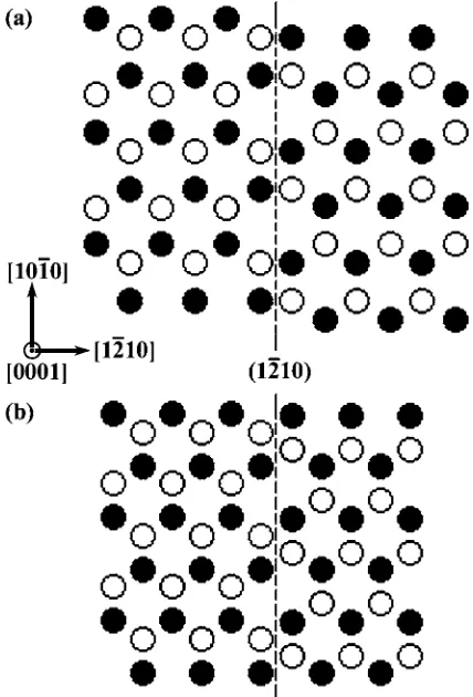
Basal plane stacking faults共BSFs兲 in the wurtzite struc-ture can be treated as planar defects forming locally the ABC cubic structure within the usual…ABABAB…stacking se-quence. Three types of BSFs can exist in a wurtzite structure: two intrinsic共I1 andI2兲and one extrinsic 共E兲13The I
1 type BSF is formed either by removal or insertion of a basal plane with further 1 / 3具11¯00典 slip of one part of a crystal with respect to the other to decrease the fault energy. This changes the perfect stacking sequence of …ABABABAB… to one with …ABABABCBCBC… 关Fig. 1共a兲兴. The single cubic
stacking ABC is in bold. Such a fault has to be bounded by a sessile Frank-Shockley dislocation with Burgers vector b= 1 / 6具202¯3典. The I2 type fault having the …ABABABCACACA… 关Fig. 1共b兲兴 stacking sequence can be formed by 1 / 3具11¯00典 shear of one part of a crystal with respect to the other or by dissociation of a perfect dislocation
共b= 1 / 3具112¯0典兲 into two Shockley partials with b = 1 / 3具11¯00典. The E-type BSF with a stacking sequence …ABABABCABABAB…关Fig. 1共c兲兴appears due to inser-tion of an extra basal plane. This type of fault is bounded by Frank partials withb= 1 / 2关0001兴.
The energy of BSFs ␥ is proportional to the number of cubic bilayers in the particular fault. As described I1-, I2-, andE-type defects consist of one, two, and three cubic bi-layers, respectively, and their energy to a first approximation is␥E⬇
3
2␥I2⬇3␥I1. Although theI1-type BSF has the lowest energy, its formation requires removal of a basal bilayer in addition to the basal shear of 1 / 3具11¯00典. This means that the I1 BSF is likely to be formed during the growth process. Deformation caused by stress during or after growth can cause formation of theI2-type BSF by movement of a glissile
Shockley partial dislocation in the basal plane. The high-energy E-type BSF is formed by precipitation of point de-fects on the basal plane. This type of fault is always sur-rounded by a dislocation loop. If 1 / 3具11¯00典shear occurs on the basal plane, such a high-energy fault can be converted into a low-energyI1fault.14
One more type of intrinsic BSF in which one of the A or B bilayers occupies the “wrong” C position was predicted theoretically by Stampfl and Van de Walle.15Such a fault would, for example, have a stacking sequence …ABABABCBABAB…关Fig. 1共d兲兴. The authors calculated that this fault would have the second-lowest formation en-ergy afterI1.
Stacking faults are also possible on planes other than thec plane. Faults formed on prismatic兵¯121¯0其planes were iden-tified by Drum.16 in AlN crystals关Fig. 2共a兲兴. From the dif-fraction conditions under which defect contrast vanishes in TEM micrographs, it was deduced that these prismatic stack-ing faults共PSFs兲 on the共¯121¯0兲 plane have the fault vector
R= 1 / 2关101¯1兴. PFSs were found to terminate BSFs. Stair-rod dislocations were observed at the intersections of PSFs and BSFs, since the intersecting faults had different fault vectors. The faults on prismatic planes in wurtzite ZnS have been reported by Amelinckx’s group.14The structural model
FIG. 1. Atomic models of basal stacking faults共BSFs兲within the wurtzite structure projected onto the共112¯0兲 plane:共a兲 I1type, 共b兲I2type,共c兲Etype共d兲I3type. Stacking sequences are indicated. Large and small circles represent Ga and N atoms, respectively.
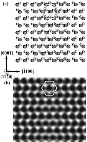
FIG. 2. Atomic models of共a兲a共12¯10兲prismatic stacking fault
of these defects, often called in the literature a stacking mis-match boundary 共SMB兲 with R= 1 / 6关202¯3兴, has been proposed,14 as shown in Fig. 2共b兲. It was noted that SMBs never end inside the crystal but rather constitute folded ar-rangements with BSFs. In this case stair-rod dislocations are not observed because SMBs have the same fault vectors as BSFs. High-resolution electron microscopy studies of AlN and AlGaN layers grown on 共0001兲 6H-SiC and sapphire substrates17,18 showed that more than 90% of the faults formed on prismatic planes had the structure proposed by Drum.16 Calculations of atomic structure for PSFs indicated that there are no wrong or broken bonds, but because of large distortions from the tetrahedral bonding the formation energy was estimated to be 72 meV/ Å2 共i.e., 1153 erg/ cm2兲.19 It was found that the PSF model proposed by Drum16is ener-getically more favorable than the SMB model proposed by Amelinckx.14
III. EXPERIMENT
The AlN buffer layer and the GaN epilayer were sequen-tially grown on a 12 mm⫻12 mm square 4H-SiC共112¯0兲 substrate in a cold-walled, vertical, pancake-style organome-tallic vapor phase epitaxy共OMVPE兲system.20 The 100 nm thick AlN buffer layer and the 1m thick undoped GaN layer were grown at 20 Torr at temperatures of 1100 °C and 1015 °C, respectively. The precursor species of trimethylalu-minum, triethylgallium, and ammonia with mass flow rates of 5.4mol/ min, 101mol/ min, and 0.14 mol/ min, re-spectively, were mixed with high-purityH2共3 slm兲in a 2 in. internal diameter sleeve located 2 in. above the substrate.
Samples were studied by conventional transmission elec-tron microscopy共TEM兲and high-resolution electron micros-copy 共HREM兲 using JEOL 3010 and JEOL ARM micro-scopes operated at 300 kV and 800 kV, respectively. The JEOL 3010 and the JEOL ARM microscopes had point-to-point resolutions of 2.1 Å and 1.5 Å, respectively, and a tilting capability ±40°. Other microscope parameters were as follows: spherical aberration Cs= 1.4 mm and Cs= 2.0 mm, chromatic aberrationCc= 2.2 mm andCc= 3.0 mm, spread of focus⬃100 Å and⬃120 Å, beam convergence angle⬃0.65 and⬃0.85 mrad, and Scherzer defocus −63.5 and −52.5 nm respectively. Cross-sectional and plan-view samples for these studies were prepared by mechanical polishing followed by dimpling down to 10m and Ar ion milling at 5 kV until perforation occurred.
HREM images were recorded near Scherzer defocus in order to compare them to simulated ones. Crystal kit and
MACTEMPAS software were used for high-resolution image simulation utilizing the multislice method.21 Tables of HREM images, including defocus versus thickness, were cal-culated in order to obtain the best matching with the experi-mental images.
IV. RESULTS AND DISCUSSION
A. Epitaxial relationships
The epitaxial relationships between the deposited GaN/ AlN layers and 4H-SiC substrate were studied by
cross-sectional TEM. Selected area electron-diffraction
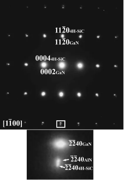
共SAED兲 patterns recorded at the 关11¯00兴 zone axis show that the AlN and GaN layers have the same orientation as the substrate. Epitaxial relationships can be written as follows: 共112¯0兲GaN储共112¯0兲AlN储共112¯0兲4H-SiC and关11¯00兴GaN储关11¯00兴AlN储关11¯00兴4H-SiC共Fig. 3兲.
B. Basal stacking faults and dislocation density
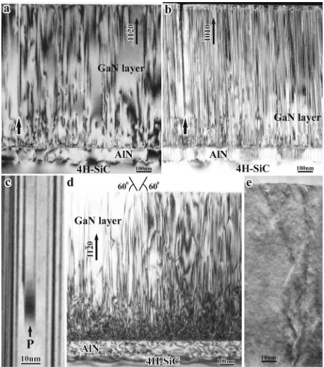
A bright field image of a cross-sectional sample 关Fig. 4共a兲兴recorded for two beam conditions with g-vector 112¯0 close to the 关11¯00兴 zone axis shows dislocations with Bur-gers vector components parallel to关112¯0兴. These are partial dislocations withb= 1 / 3关101¯0兴and b= 1 / 3关011¯0兴 terminat-ing BSFs. In order to brterminat-ing BSFs into strong contrast it is necessary to tilt the specimen in thecplane by +30° or −30° from关11¯00兴toward关¯2110兴or关12¯10兴zone axis, respectively, so thatg= 011¯0 org= 1¯010. For the image obtained under the g= 1¯010 diffraction condition关Fig. 4共b兲兴the contrast typical for BSFs共defects arranged perpendicular to the substrate兲is clearly seen. The majority of BSFs are nucleated at the 4H− SiC/ AlN interface and propagate through the AlN and the GaN layers to the sample surface.
TEM 共112¯0兲 plan-view samples have also been investi-gated in order to measure dislocation density. The plan-view
FIG. 3. Selected area electron diffraction pattern recorded from a cross-sectional sample along the关11¯00兴 zone axis, showing the epitaxial relationship between GaN layer and the SiC substrate.
configuration is also more suitable for HREM structural studies of BSFs with the关112¯0兴 zone axis, since these de-fects are in edge-on configuration and tilting of the specimen by a large angle is not required. For this zone axis, configu-ration BSFs are visible as thin lines parallel toc planes of GaN when bright field images were obtained under a two beam condition withg= 11¯00关Fig. 5共a兲兴. The measured den-sity of the BSFs was⬃1.6⫻106cm−1. Such a high density of BSFs results in streaking of diffraction spots in the关0001兴 direction on selected area electron-diffraction patterns re-corded along the 关112¯0兴 zone axis 关Fig. 6共a兲兴. Some of the BSFs continue through the whole field of view, while others are terminated by partial dislocations. Some of such termi-nations are marked by black and white arrows关Figs. 5共a兲and 5共d兲and, 5共e兲兴. The image on Fig. 5共b兲, obtained under the two-beam condition forg= 0002, is taken from the same area of the sample as the image on Fig. 5共a兲. Black and white arrows on Fig. 5共b兲point to the same BSF terminations as on
Fig. 5共a兲. Stacking faults are out of contrast for two beam imaging conditions withg= 0002, therefore we can observe different contrast behavior of partial dislocations marked by black and white arrows. Namely, partial dislocations bound-ing BSFs marked with black arrows are in contrast on Fig. 5共b兲, whereas dislocations marked with white arrows are out of contrast on the same image 关also see an enlargement in Fig. 5共g兲and Fig. 5共h兲兴. Under the above imaging conditions one can draw a conclusion that two types of dislocations are present in the sample: the first one, which has a component of Burgers vector parallel to关0001兴 共black arrows兲, and the second one, which has no component of Burgers vector along关0001兴. As it will be shown in the next paragraph the first type of dislocations are bounding I1 BSFs and the sec-ond type are boundingI2BSFs. The densities of these dislo-cations are⬃4.0⫻1010 cm−2and⬃0.4⫻1010cm−2, respec-tively.
Figure 7 shows characteristic HREM images of BSFs re-vealed in the sample. According to the observed stacking sequences the first two images关Figs. 7共a兲and 7共b兲兴represent
FIG. 4. Cross-sectional TEM images:共a兲bright field image共g
= 112¯0兲 showing distribution of dislocations with Burgers vector components parallel to 关112¯0兴. 共b兲 Dark field image 共g= 1¯010兲 showing that basal stacking faults nucleate at the 4H-SiC/ AlN in-terface and propagate through the GaN to the sample surface. A crack formed approximately 100 nm from the AlN buffer layer is marked by an arrow.共c兲Bright field image共g= 1¯010兲of an inclined prismatic stacking fault共P兲bounded by two basal stacking faults.
共d兲 Bright field image 共g= 112¯0兲 taken close to the 关0001兴 zone axis. Prismatic stacking faults formed in共2¯110兲or共12¯10兲 are vis-ible as thin lines coming to the sample surface at a 60° angle.共e兲 Higher magnification image recorded under a many beam diffrac-tion condidiffrac-tion showing zigzaglike configuradiffrac-tion of a prismatic stacking fault, which results in an almost vertical propagation of the latter from substrate to the sample surface.
FIG. 5. Bright field TEM images of a plan-view sample ob-tained with two perpendicularg-vectors:共a兲g= 11¯00; parallel lines represent stacking faults formed on the basal plane of GaN.共b兲 g
I1-type BSFs with the sequences…ABABABCBCBC…and …ABABACACAC…, respectively. These I1-type BSFs are formed due to removal关Fig. 7共a兲兴or insertion关Fig. 7共b兲兴of a basal plane followed by 1 / 3关11¯00兴or 1 / 3关1¯100兴slip of the upper part of the GaN crystal with respect to the lower part and are bounded by sessile Frank partial dislocations. By placing a Burgers circuit around the end of the fault one can find that the Frank partial dislocation terminating the BSF has the vectorb= 1 / 6关22¯03兴when a basal plane is removed. The fault with the opposite sign of the Burgers vector b = 1 / 6关¯2203¯兴will appear when a basal plane is inserted. The I2-type BSF with the sequence of…ABABABCACACA… was also revealed关Fig. 7共c兲兴. This type of BSF is necessarily bounded by two glissile Shockley partial dislocations with opposite Burgers vectors 共b= 1 / 3具11¯00典兲 关see also Fig. 9共c兲兴.22
Figure 7共d兲 shows an I3-type BSF characterized by the
…ABABABCBABAB… stacking sequence, where one of
the A or B bilayers is “switched” to the C position. This type of fault can also be treated as twoI1BSFs forming a nanot-win of a cubic structure. The incorporation of the firstI1BSF into the wurtzite structure would change the stacking se-quence from the original …ABAB… into …BCBC…, but the second I1 BSF would immediately revert the stacking sequence back to the original configuration. It is important to recall the theoretical prediction that only the I1 fault has lower energy than theI3 fault.15We have not observed any termination by partial dislocations for this kind of BSF. These faults are also responsible for the appearance of extra diffraction spots on the关112¯0兴zone axis SAED关Fig. 6共b兲兴. These diffraction spots correspond to a double GaN unit cell in the关0001兴direction.
It should be noted at this point that noE-type BSFs were observed in this sample. This absence can be ascribed to the fact that the formation energy for theE-type BSF is higher than that of the other fault types.
C. Prismatic stacking faults
Partial dislocations are not the only way to terminate BSFs. Earlier studies14,16 showed that BSFs can be termi-nated by PSFs. An example of such termination within the GaN layer is shown in Fig. 4共c兲. Imaging conditions are set for BSFs to be in a strong contrast. The area “P” between two BSFs has a characteristic contrast of a PSF inclined at some angle to the image plane. These PSFs are visible in edge-on configuration in bright field images obtained for g = 112¯0 close to 关0001兴as thin lines intersecting the sample surface at a 60° angle关Fig. 4共d兲兴. Some of PSFs propagate to the sample surface. Under higher magnification关Fig. 4共e兲兴it is possible to see that PSFs formed on 共¯2110兲 and 共12¯10兲 planes exhibit a zigzaglike structure because of severe face-ting on共¯2110兲/共12¯10兲planes. It is assumed that such zigza-glike behavior, which results in an almost vertical propaga-tion of the PSFs from substrate to the sample surface, decreases the total energy of the above PSFs.
In addition to cross-sectional images, PSFs are also re-vealed in view images. Areas marked by circles in plan-view images关Figs. 5共a兲, 5共b兲, 5共f兲, and 5共h兲兴represent PSFs formed on共¯2110兲and共12¯10兲planes intersecting the sample surface at a 60° angle. The estimated density of the PSFs from plan-view bright field images is⬃0.7⫻102cm−1. Each of their boundaries in thec planes acts as a termination or nucleation site for a basal stacking fault 关Fig. 5共a兲兴. The separation between two BSFs terminated at a 共¯2110兲 or
共12¯10兲PSFs usually does not exceed 6–7 nm, which gives us the characteristic size of a PSF in the关0001兴direction.
A characteristic high-resolution image of a 共¯2110兲 PSF obtained near the Scherzer defocus is shown on Fig. 8共a兲. In
FIG. 7. High-resolution images of a plan-view sample showing typical basal stacking faults observed:共a兲 removal of basal plane followed by 1 / 3关11¯00兴 slip generates the I1 basal stacking fault
bounded by a sessile Frank partial dislocation with the Burger vec-torb= 1 / 6关22¯03兴.共b兲 Insertion of an extra basal plane also results in generation of the low-energyI1basal stacking fault bounded by a sessile Frank partial dislocation withb= 1 / 6关2¯203¯兴.共c兲Shear dis-placement in the关11¯00兴direction leads to formation of theI2basal stacking fault, which is bounded by a glissile Shockley partial dis-location.共d兲“Switching” of A or B bilayer to the C position results in formation of theI3basal stacking fault. Stacking sequences for
each basal stacking fault is shown at the left. FIG. 6. 共a兲 Selected area electron diffraction pattern recorded
from a plan-view sample along the关112¯0兴zone axis. Streaking of diffraction spots along the关0001兴direction arises due to the large number of basal stacking faults.共b兲Enlarged part of the diffraction pattern showing additional spots arising from doubled c unit lattice of GaN共marked by white arrows兲.
order to determine the atomic structure of the defect experi-mental and simulated HREM images were compared. Two models, one of a prismatic stacking fault 共PSF兲 关Fig. 2共a兲兴 and one of a stacking mismatch boundary共SMB兲 关Fig. 2共b兲兴, were calculated. Since size of PSFs in the关0001兴 direction does not exceed 6–7 nm, as was measured from plan-view images, simulations were done near Scherzer defocus for sample thicknesses up to 7 nm. Simulated HREM images of PSF and SMB calculated for defocus of −45 nm and sample thickness of 4.7 nm are shown in Figs. 8共b兲and 8共c兲, respec-tively. The simulated image关Fig. 8共b兲兴of PSF shown on Fig. 2共a兲has the closest match to the experimental HREM image shown on Fig. 8共a兲. The same model of PSF 共earlier pro-posed by Drum16was calculated by Northrup19who showed that the PSF is energetically more favorable than the SMB.
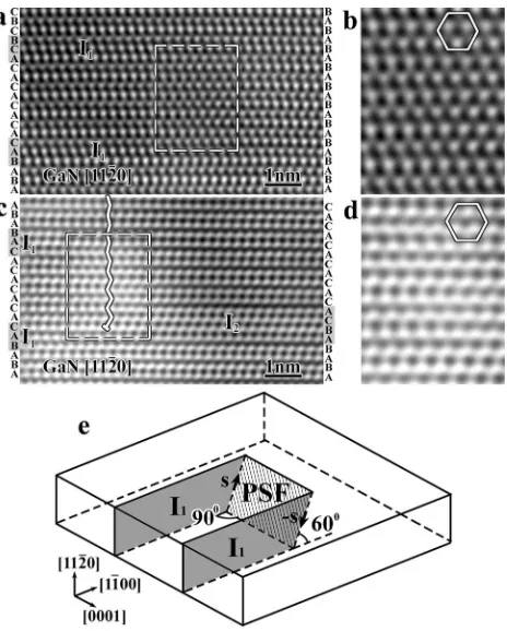
A HREM image of a PSF formed on 共¯2110兲 or 共12¯10兲 planes intersecting the共112¯0兲sample surface at a 60° angle is shown in Fig. 9共a兲. The inclined defect reveals itself in hexagonal-like contrast 关Fig. 9共b兲兴 extending over approxi-mately six共11¯00兲interplanar distances between twoI1-type BSFs 关the area marked by a dashed box on Fig. 9共a兲兴. We arbitrarily assigned …ABAB…, as the perfect hexagonal stacking sequence, to atomic columns to the left and right sides of the PSF at the bottom part of the image, where the undisturbed structure is revealed关see the assigned letters on both sides of Fig. 9共a兲兴. As soon as the firstI1-type BSF is introduced, it changes the perfect stacking to …ACAC…
FIG. 8. 共a兲 High-resolution image recorded down to the
关0001兴GaNzone axis of a prismatic stacking fault formed in共¯2110兲 or 共12¯10兲. 共b, c兲 High-resolution image simulations 共defocus −45.0 nm; thickness 4.7 nm兲:共b兲based on Drum’s prismatic stack-ing fault model关Fig. 2共a兲兴, and共c兲 based on Amelinkx’s stacking mismatch boundary关Fig. 2共b兲兴.
FIG. 9. 共a兲Plan-view high-resolution image of an inclined pris-matic stacking fault共PSF兲 共inside dashed box兲 projected onto the
共112¯0兲plane revealing hexagonal-like contrast. The PFS terminates twoI1basal stacking faults. Stacking sequences on the right and left
sides of the image show the 1 / 2关0001兴shift induced by the inclined PSF. The firstI1changes the stacking sequence from…ABAB…to
…ACAC…. This sequence is preserved until the second I1 BSF converts it to…BCBC….共b兲Magnified area inside dashed box in
共a兲.共c兲 Plan-view HREM image of PSF, which terminates twoI1
BSFs. Stacking sequences on the right and left sides are shown. No net displacement in关11¯00兴induced by BSFs is observed. Although the initial …ABAB… stacking sequence changes to …CACA… when crossing the firstI1boundary, the secondI1boundary restores the initial…ABAB…stacking sequence. A Shockley partial dislo-cation 共1 / 3具11¯00典兲, which arises from the termination of the I2
basal stacking fault, is also marked. A second dislocation with an opposite Burgers vector is located to the right, outside the image frame.共d兲Magnified area inside dashed box in 共c兲. 共e兲 Schematic representation of termination of two I1 BSFs by PSF, s and −s
关left-hand side of Fig. 9共a兲兴. This stacking sequence is kept in the region between twoI1-type BSFs bounding the PSF. To the left side of the PSF there is an …ACAC… sequence, while the stacking sequence to the right of the same defect is …ABAB…. This is an indication of a 1 / 2关0001兴 shift be-tween the left and right parts of the crystal separated by the PSF characterized by a displacement vector R= 1 / 2具101¯1典
关see Figs. 2共a兲, 8共a兲, and 8共b兲兴.
In order to calculate the contrast on a HREM image pro-duced by such a defect, image simulations have been carried out using super cells of an inclined PSF lying at a 60° angle to the共112¯0兲sample surface plane关Fig. 10共a兲兴. Because of a shift between the upper and lower parts of the crystal sepa-rated by the PSF, atoms in the overlaying region are pro-jected in a hexagonal-like way, which gives rise to a hexagonal-like contrast visible on the simulated HREM im-age关Fig. 10共b兲兴calculated with a defocus value of −57.5 nm and foil thickness of 3 nm. This correlates well with the experimental image shown in Fig. 9共a兲. The foil thickness on this experimental HREM image can be estimated from a simple geometry as
t=xtg共60 °兲, 共1兲
wherexis the PSF projection width on the共112¯0兲plane. As mentioned earlier, the PSF projection width extends over ap-proximately six 共11¯00兲 interplanar distances. Inserting x
=6d11¯00, whered11¯00= 0.28 nm is the lattice interplanal dis-tance in the 关11¯00兴 direction, into Eq. 共1兲, we obtain t = 2.9 nm for the experimental sample thickness.
The same type of hexagonal-like contrast is revealed be-tween twoI1BSFs in Fig. 9共c兲. The area of the inclined PSF is marked by a dashed box and shown magnified in Fig. 9共d兲 with superimposed hexagon illustrating hexagonal-like be-havior of the observed contrast. Note, that the Shockley par-tial dislocation shown on the Fig. 9共c兲terminates theI2-type BSF. Another Shockley partial with the opposite Burgers vector terminates theI2somewhere on the right, outside the image frame.
D. Stair-rod dislocations
Since the displacement vectors ofI1BSF and PSF are not the same, a stair-rod dislocation is expected at the intersec-tion of these two faults. Furthermore, the I1 BSF is able to assume any one of the possible 1 / 3具11¯00典displacement vec-tors that alters the stacking sequence of the lattice.
Figure 9共a兲 shows a plan-view HREM image of a PSF terminated by twoI1BSFs. As it was shown earlier the pres-ence of the inclined PSF, which comes to the共112¯0兲sample surface at a 60° angle, reveals itself in a hexagonal-like con-trast at the center of the image outlined by the dashed box. Let us assume that of the possible two sets of planes, namely,
共12¯10兲 and共¯2110兲, PSF formed on the 共12¯10兲 plane. Then the displacement vector for this PSF will be 1 / 2关101¯1兴. Fol-lowing the HREM lattice image on Fig. 9共a兲from the bottom to the top, it is seen that the stacking sequence begins as …ABAB… below the PSF. Past the first I1 boundary the sequence changes to…CACA within the region spanning the PSF关marked on the left-hand side of Fig. 9共a兲; compare to the sequence on the right-hand side兴. The difference between anI1 displacement vector 1 / 6关202¯3兴and the PSF displace-ment vector 1 / 2关101¯1兴 forms the Burgers vector b = 1 / 6关101¯0兴 for the stair-rod dislocation in the screw orien-tation. That is,
1/2关101¯1兴= 1/6关202¯3兴+ 1/6关101¯0兴.
Moving past the secondI1boundary and above the PSF, the lattice image follows the …BCBC… stacking sequence
关Fig. 9共a兲兴. In order to change the…CACA…sequence into the …BCBC…, the displacement vector for the second I1 BSF must be 1 / 6关02¯23兴. Then the stair-rod dislocation at the intersection of the PSF withR= 1 / 2关101¯0兴 with the second I1共1 / 6关02¯23兴兲 should be 1 / 6关3210兴. This stair-rod disloca-tion will fulfill the equadisloca-tion
1/2关101¯1兴= 1/6关02¯23兴+ 1/6关3210兴.
This stair-rod has mixed character with 1 / 6关101¯0兴screw and 1 / 6关22¯00兴 edge components. The 1 / 3关11¯00兴 edge compo-nent is responsible for accommodation of different sequences above the PSF.
FIG. 10. 共a兲 Drum’s atomic model 关Fig. 2共a兲兴 of a prismatic stacking fault formed in共¯2110兲or共12¯10兲planes projected onto the
共112¯0兲plane of GaN.共b兲Simulated high-resolution image共defocus −57.5 nm; thickness 3 nm兲 of inclined prismatic stacking fault based on Drum’s models shown in共a兲.
The defect geometry described above, however, is not the only possible configuration. There is another possibility when the two I1 BSFs have displacement vectors that are equal and opposite, so that no net displacement results from the presence of two such I1 BSFs bounding the PSF. This case corresponds to Fig. 9共c兲, where stacking sequence is preserved. Although the initial …ABAB… stacking se-quence changes to …CACA… when crossing the first I1 boundary, the second I1 boundary returns the initial …ABAB…stacking sequence共compare stacking sequences on the left- and right-hand sides of the micrograph兲. In this case we can write equations for displacement vectors at first and secondI1boundaries as
1/2关101¯1兴= 1/6关202¯3兴+ 1/6关101¯0兴, and
1/2关101¯1兴= 1/6关¯2023兴+ 1/6关505¯0兴, respectively.
The displacement vector 1 / 6关505¯0兴 of the stair rod is equivalent to the 1 / 6关¯1010兴. A schematic representation of termination of twoI1BSFs is illustrated in Fig. 9共e兲, wheres and −srepresent 1 / 6关101¯0兴and 1 / 6关¯1010兴stair-rod disloca-tions, respectively.
E. Stacking fault energy
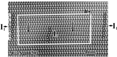
As was mentioned earlier, anI2-type BSF can be formed either by the shear of the crystal in a basal plane by 1 / 3具11¯00典 or by dissociation of a perfect dislocation into two Shockley partials. Figure 11 shows a high-resolution im-age of the I2 BSF, which is formed by dissociation of a 1 / 3具112¯0典 perfect dislocation into two Shockley partials with b= 1 / 3具11¯00典 共e.g., 1 / 3关112¯0兴→1 / 3关011¯0兴 + 1 / 3关101¯0兴兲. The positions of these partials are marked by arrows. The distance between the partials is ⬃5.5 nm. The right partial does not give a contrast from the inserted plane on this image since it has only a small component of the Burgers vector projected on the 共112¯0兲 viewing plane. A Burgers circuit placed around theI2BSF共marked in Fig. 11 by white contour兲shows the fault vectorb= 1 / 2关11¯00兴. The
I1-type BSF, which is also visible in the image, extends through the whole field of view and does not alter the circuit closure failure.
Taking the distance between dissociated dislocations and knowing the elastic constants of the crystal, it is possible to estimate the formation energy ␥ of the I2 intrinsic BSF as follows:13
␥=a2/12d, 共2兲 where is the shear moduli,a= 0.32 nm is the lattice con-stant of the wurtzite GaN, andd= 5.5 nm is the distance be-tween partials. There is a range of shear moduliavailable in the literature determined by different methods.23–28 We used several values of , such as 24.1 GPa determined by x-ray measurements,23 105 GPa, as an average of measure-ments by Brillouin scattering,24–26 81.4 GPa measured by resonant ultrasonic spectroscopy,27 and 95 GPa obtained from density-functional-theory calculations.28For the above-mentioned values of , the calculated energies ␥ were
共11.8± 1.2兲, 共52± 5兲, 共40± 4兲, and 共46.7± 4.5兲erg/ cm2, re-spectively. Errors in parentheses reflect the uncertainty in determining the exact positions of the right partial disloca-tions. The calculated energy of 40 erg/ cm2 is very close to the values of⬃41 and ⬃43 erg/ cm2 obtained theoretically by Wright29 and by Stampfl and Van de Walle.15These au-thors also suggested that stacking fault energy of other ni-trides should be higher: ⬃80 erg/ cm2 in InN and ⬃213 erg/ cm2 in AlN,29 or ⬃65 erg/ cm2 in InN and ⬃204 erg/ cm2 in AlN.15
We were unable to find other reports of stacking fault energy determined experimentally for GaN, but for InN and AlN these energies were 共41± 8兲 and 共220± 70兲erg/ cm2, respectively.30 These values were obtained using the same measurement technique for dislocation dissociation as that used in our work. Our stacking fault formation energy value of 共40± 4兲erg/ cm2 for GaN was calculated based on = 81.4 GPa. It is the best fit to the experimental values in the series of nitrides共GaN, InN, AlN兲and agrees well with the-oretical predictions.
V. CONCLUSIONS
Structural defects in nonpolar a-plane GaN grown on a 4H-SiC substrate with an AlN buffer layer have been studied by transmission electron microscopy. Specimens imaged in both plan-view and cross-sectional configurations revealed that the majority of defects are basal and prismatic stacking faults. The majority of basal stacking faults were formed at the 4H-SiC/ AlN interface and propagated into the GaN layer. Only low-energyI1,I2, andI3 types of basal stacking faults with a density of ⬃1.6⫻106cm−1 were observed in the GaN layers. Stacking faults of I1 andI2 types were ter-minated by sessile Frank-Shockley and glissile Shockley par-tial dislocations with Burgers vectors b= 1 / 6具22¯03典 and b = 1 / 3具11¯00典. The densities of these partial dislocations at the surface of the GaN layer were ⬃4.0⫻1010cm−2 and⬃0.4 ⫻1010cm−2, respectively. I3 basal stacking faults were ob-served experimentally. Based on the high-resolution image
FIG. 11. High-resolution image of a dissociated 1 / 3具112¯0典 per-fect dislocation into two Shockley partials共1 / 3具11¯00典兲 bounding the I2 basal stacking fault. Arrows indicate the positions of the partials. The Burgers contour placed around the I2 BSF shows a
simulations of prismatic stacking faults we were able to show their formation on 共12¯10兲 or 共¯2110兲 planes of GaN. These simulations also confirmed the atomic model for pris-matic stacking faults proposed earlier by Drum.17 Because the PSF has very large fault energy, it dissociates into two low-energyI1 basal stacking faults with accommodation of the difference between fault vectors at each of two BSF/PSF intersections by a stair-rod dislocation. Separation of Shock-ley partial dislocations was used to estimate the stacking fault energy for the I2-type defect in GaN. The estimated
value was observed to be in good agreement with theoretical calculations and experimentally determined values for differ-ent nitrides.
ACKNOWLEDGMENTS
This work was supported the Air Force Office of Scien-tific Research共Dr. G. Witt兲under the Order No. OGMORD 52K44134. The use of the facilities at the National Center for Electron Microscopy at Lawrence Berkeley National Labo-ratory is greatly appreciated.
*Correspondence author; Email: [email protected]
1S. Nakamura, Science 281, 956共1998兲.
2M. A. Khan, J. W. Yang, G. Simin, R. Gaska, M. S. Shur, and A.
D. Bykhovski, Appl. Phys. Lett. 75, 2806共1999兲.
3T. Nishida and N. Kobayashi, Phys. Status Solidi A 188, 113 共2001兲.
4F. Bernardini and V. Fiorentini, Phys. Rev. B 57, R9427共1998兲. 5I. Jin Seo, H. Kollmer, J. Off, A. Sohmer, F. Scholz, and A.
Hangleiter, Phys. Rev. B 57, R9435共1998兲.
6T. Deguchi, K. Sekiguchi, A. Nakamura, T. Sota, R. Matsuo, S.
Chichibu, and S. Nakamura, Jpn. J. Appl. Phys., Part 238, L914
共1999兲.
7P. Waltereit, O. Brandt, A. Trampert, H. T. Grahn, J. Menniger,
M. Ramsteiner, M. Reiche, and K. H. Ploog, Nature共London兲
406, 865共2000兲.
8E. Kuokstis, C. Q. Chen, M. E. Gaevski, W. H. Sun, J. W. Yang,
G. Simin, M. Asif Khan, H. P. Maruska, D. W. Hill, M. C. Chou, J. J. Gallagher, and B. Chai, Appl. Phys. Lett. 81, 4130共2002兲.
9H. M. Ng, Appl. Phys. Lett. 80, 4369共2002兲.
10M. D. Craven, P. Waltereit, W. Feng, J. S. Speck, and S. P.
Den-Baars, Jpn. J. Appl. Phys., Part 2 42, L235共2003兲.
11B. A. Haskell, F. Wu, S. Matsuda, M. D. Craven, P. T. Fini, S. P.
DenBaars, J. S. Speck, and S. Nakamura, Appl. Phys. Lett. 83, 1554共2003兲.
12J. Jasinski, Z. Liliental-Weber, H. P. Maruska, B. H. Chai, D. W.
Hill, M. M. C. Chou, J. J. Gallagher, and S. Brown, Mater. Res. Soc. Symp. Proc. 764, 369共2003兲.
13D. Hull and D. J. Bacon,Introduction to Dislocation共Pergamon
Press, Oxford, 1984兲.
14H. Blank, P. Delavignette, R. Gevers, and A. Amelinckx, Phys.
Status Solidi 7, 747共1964兲.
15C. Stampfl and C. G. Van de Walle, Phys. Rev. B 57, R15052 共1998兲.
16C. M. Drum, Philos. Mag. 11, 313共1965兲.
17P. Vermaut, G. Nouet, and P. Ruterana, Appl. Phys. Lett. 74, 694 共1999兲.
18P. Ruterana, B. Barbaray, A. Bere, P. Vermaut, A. Hairie, E.
Paumier, G. Nouet, A. Salvador, A. Botchkarev, and H. Morkoc, Phys. Rev. B 59, 15917共1999兲.
19J. E. Northrup, Appl. Phys. Lett. 72, 2316共1998兲.
20B. P. Wagner, E. A. Preble, Z. J. Reitmeier, R. F. Davis, D. N.
Zakharov, and Z. Liliental-Weber, Mater. Res. Soc. Symp. Proc.
798, 375共2004兲.
21Programs are available from http://www.totalresolution.com 22V. Potin, P. Ruterana, and G. Nouet, J. Phys.: Condens. Matter
12, 10301共2000兲.
23V. A. Savastenko and A. U. Sheleg, Phys. Status Solidi A 48,
K135共1978兲.
24Y. Takagi, M. Ahart, T. Azuhata, T. Sota, K. Suzuki, and S.
Na-kamura, Physica B 219–220, 547共1996兲.
25A. Polian, M. Grimsditch, and I. Grzegory, J. Appl. Phys. 79,
3343共1996兲.
26M. Yamaguchi, T. Yagi, T. Azuhata, T. Sota, K. Suzuki, S.
Chichibu, and S. Nakamura, J. Phys.: Condens. Matter 9, 241
共1997兲.
27R. B. Schwarz, K. Khachaturyan, and E. R. Weber, Appl. Phys.
Lett. 70, 1122共1997兲.
28A. F. Wright, J. Appl. Phys. 82, 2833共1997兲. 29A. F. Wright, J. Appl. Phys. 82, 5259共1997兲.
30K. Suzuki, M. Ichihara, and S. Takeuchi, Jpn. J. Appl. Phys., Part
1 33, 1114共1994兲.