Mode Splitting Based on the Coupling between Modes of Two
Nanodisks Cavities and a Plasmonic Waveguide
Mohamed Nady*
Abstract—A metal-insulator-metal (MIM) plasmonic waveguide coupled with two nanodisks as a resonator has been examined and numerically simulated with the finite-difference time-domain (FDTD) and analytically by the Temporal Coupling Mode Theory (CMT). Based on the three-level system, the strong destructive interference between the two resonators leads to the distinct mode splitting response. The characteristics of mode splitting show that there is anomalous dispersion with the novel fast-light feature at the resonance. Meanwhile, the slow light characteristic can also be achieved in the system at wavelengths of the split modes. The relationship between the transmission characteristics and the geometric parameters is examined. The results show that the modulation depth of the mode splitting transmission spectrum of 80% with 0.175 ps fast-light effect of resonance can be achieved, while for the two modes these values are around 30% with−0.18 ps slow light-effect. There is a good agreement between the FDTD simulated transmission features and CMT. The characteristics of the system indicate critical potential applications in integrated optical circuits such as slow-light and fast-light devices, optical monitoring, an optical filter, and optical storage.
1. INTRODUCTION
Plasmonics; The Promise of Highly Integrated Optical Devices play an important role in routing, switching and controlling of light in a large number of fields of modern optical communication and networks [1, 2]. In the plasmonic waveguides there is a coupling between the transferred electromagnetic waves and the surface collective oscillations of free electrons in a metal; therefore, it is known by Surface Plasmon Polaritons (SPPs). The SPP waves are bound to and propagate along the metal-dielectric-metal interfaces [2]. The light confinement below the diffraction limit is the competitive advantage of plasmonic waveguide compared to other types of optical waveguides such as photonic crystals, optical fibers, etc. Furthermore, the introduction of deep-submicron technologies in electronic engineering leads to a revolution in optoelectronic circuits [3] and membrane technology [31]. A Huge number of structures are introduced by transporting SPPs such as grooves and wedges [4, 5], Domino plasmon waveguide [6, 7], Metal-Insulator-Metal waveguides (MIM) [8], and thenano-particle plasmon waveguides [9]. In addition to the high degree of SPP confinement, compact size and fabrication simplicity have made MIM geometry the most used structure among other nano-scale waveguides [10]. Different types of plasmonic filters such as tooth-shaped subwavelength and add-drop topologies are introduced and analyzed by numerical methods such as Finite-Difference Time-Domain (FDTD) and finite element method (FEM) [11, 12]. It has been shown that the transmission spectra of these structures can generate a narrow bandpass filter [12]. Moreover, ring resonator filters generate opposite phase standing waves using optical cavities, for use in the suppression of some specific wavelengths in the transmission spectrum [13]. Depending on the position of cavities relative to the main MIM guiding structure, it is possible to achieve bandpass (two parallel MIM waveguides coupled to each other by a circular ring resonator) or band-stop filters (two
Received 14 February 2017, Accepted 25 March 2017, Scheduled 9 April 2017
based on the MIM waveguide with periodic grooves [20] and wavelength de-multiplexer based on MIM plasmonic nano-capillary resonators [21]. However, there are some limits in these structures such as huge dimensions to splitting functionality, low transmittance, power leakage, and maximum fanout of two for splitter channels [19–21].
Mode splitting of surface plasmon resonance has a great significance in many applications especially in integrated optics. Different structures are proposed to achieve mode splitting such as mode splitting in a super-period metal nanohole array grating [22]. But the transmission values of the split modes are much different. This paper introduces a novel nanoscale plasmonic mode splitting while its functionality is verified by CMT and FDTD in different configurations. This paper is organized as follows. Section 2 introduces the CMT Design of two nanodisks coupled with the plasmonic waveguide. Section 3 describes the FDTD modeling of proposed structure and introduces the numerical results. The transmission characteristics with varying geometric parameters are introduced in Section 4. Finally, Section 5 summarizes our concluded remark.
2. CMT DESIGN OF TWO NANODISKS COUPLED WITH PLASMONIC WAVEGUIDE
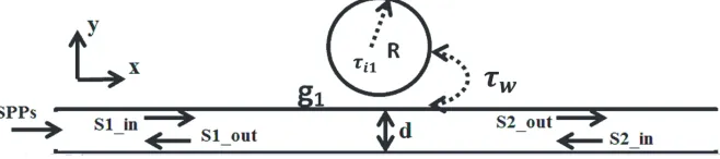
The MIM plasmonic waveguide coupled with a nanodisk resonator shown in Fig. 1 is a well-known structure, and the nanodisk is to satisfy the theoretical resonant equation given by [23]
kd
H(1)
n (kmR)
Hn(1)(kmR)
=km
J(1)
n (kdR)
Jn(1)(kdR)
kd,m=k √
εd,m
(1)
where k is the wave number, and it includes a relatively small negative imaginary part which stands for the loss. kd,m are the wave vectors in the metal and the dielectric nanodisk, respectively. εd is the
relative dielectric constant of the dielectric and εm the relative dielectric constant of the metal, which
can be obtained from the Drude model. R represents the radius of the nanodisk cavity. Hn and H n
are the first kind Hankel function with order n and its derivation, and Jn and Jn are the first kind
Bessel function with ordern and its derivation, respectively. The first and second orders of Bessel and Hankel functions correspond to the first- and second-order modes that resonate inside the nanodisk. It is obvious from Eq. (1) that the resonance wavelength λ0 depends on radius R and the refractive index. The width of the bus waveguide is set at d= 0.05µm which is small enough compared to the wavelength of the incident light. Therefore, only the fundamental mode of the waveguide is taken into consideration [24]. As the signal passes through the system, the wavelength which satisfies the resonant condition of the nanodisk, Eq. (1), will be confined in the nanodisk and coupled back into the waveguide output. So, the obvious stop-pass filtering effect should be observed in the waveguide-resonator system, as shown in Fig. 2. As expected, the light can be confined in the resonator when the wavelength of λ is equal to 1.084µm, and the corresponding transmission dip of 30% can be achieved.
(a) (b) λ=1.038 μm
(c) λ=1.158 μm (d) λ=1.084 μm
Figure 2. (a) Transmission spectrum of the proposed structure in Figure 1 with R = 276 nm, g1= 11 nm, (b)–(d) contour map of the magnitude of the magnetic field distribution for the structure.
To make this phenomenon more clear, the magnitudes of the magnetic field distributions at wavelengths λ= 1.038,1.158, and 1.084µm are displayed in Figs. 2(b), (c) & (d). It is obvious from these figures that the energy is highly coupled into the nanodisk at the resonance wavelength result in the weak magnetic distributions in the bus waveguide (see Fig. 2(d)).
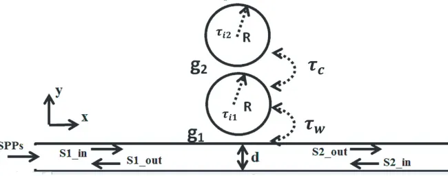
2.1. Mode Splitting Based on the Plasmonic Waveguide Coupled with Two Nanodisks
The proposed schematic illustration of the new system is shown in Fig. 3. Compared with Fig. 1, the only difference is that we add a new nanodisk on the top of nano resonator. The radius of this new nanodisk is assumed to be equal to the radius of the first one. The material of the bus waveguide and the two nanodisks are assumed to be air. The background metal is silver, and its dispersive permittivity can be denoted by the Drude model [24]
ε(ω) =ε∞−ω2p ω2+iωγ (2)
whereω is the angular frequency of the incident light, ε∞ the dielectric constant at an infinite angular frequency and equals 3.7, ωp the bulk plasma frequency and equals 9.1 eV, and γ the electron collision
frequency equals 0.018 eV. The surface plasmon polaritons (SPPs) is excited at the metallic surface and confined in the plasmonic waveguide when a TM light is entered into the waveguide [25]. When the SPPs waves go through the waveguide, the energy can be coupled directly into the first nanodisk and then coupled between the first and second nanodisks.
0 0
A1&A2 are the mode amplitudes of first and second nanodisks, respectively; S1,in, S2,out, S1,out are
the incident/transmitted/reflected waveguide mode amplitudes, which are normalized such that their squared values correspond to the incident/transmitted/reflected/dropped power; 1/τi1,1/τi2&1/τw are
decay rates due to intrinsic loss for the two nanodisks and waveguide coupling loss, respectively; Qi1, Qi2&Qw are cavity quality factors related to intrinsic loss at the nanodisks and the waveguide
coupling loss, respectively; Qtis total quality factor (1/Qt= 1/Qi1+1/Qi1+ 1/Qw). Here,Qw denotes
the nanodisk-waveguide coupling and is referred to as “waveguide coupling quality factor”, whereasQc
represents the nanodisk-nanodisk coupling and is referred to as “disk coupling quality factor”. The decay rates relate to the cavity quality factors byQie=ω0τie/2; (e= stands for 1or2) andQw=ω0τw/2. And the
coupling coefficient between the two cavity modes is denoted byτcwhich relates to disk coupling quality
factor byQc=ω0τc/2. δ is used to normalize the frequencyω, which is defined byδ = (ω−ω0)/ω0, and
t=S2,out/S1,in&r =S1,out/S1,in to denote transfer functions for the transmitted port and the reflected
port, respectively. The transmission T, effective phase shift θ and group delay τ can be calculated as T =abs(t2), θ= arg(t) and τ =dθ(ω)/dω, respectively. The CMT equations are given as follows:
dA1
dt =
jω0− 1 τi1 −
1 τw
A1+
1 τw
S1,in−jμA2 (3)
dA2
dt =
jω0− 1 τi2
A2−jμA1 (4)
Due to energy conservation, the relationship of the incoming and outgoing lights in the bus waveguide can be denoted as
S1,out = S2,in+j √
αA1 (5)
S2,out = S1,in+j √
αA1 (6)
If a sinusoidal harmonic oscillation, e−iωt, is assumed, then dA/dt = −iωA. Plugging this and S2,in= 0 into Equations (3) and (4), the transfer functiont=S2,out/S1,incan be obtained as follows:
t= 1− jδω0τw+τw/τi2
2 τc
2 +
j2δω0+ 1 τi1
+ 1
τi2
+ 1 τw 2 − 1 τi1 −
1 τi2
+ 1
τw
2 (7)
It is useful to write this transfer function in terms of quality factorsQinstead ofτ
t= 1− (j2δ+ 1/Qi2) /Qw
1 Qc
2 +
j2δ+ 0.5 Qi1
+ 0.5 Qi2
+ 0.5 Qw 2 − 0.5 Qi1 −
0.5 Qi2
+ 0.5 Qw
2 (8)
For simplicity, letτi2 = 0 or Qi2 =∞. From Eq. (8) and the definition of transmission T, we can obtain an expression ofT as
T = 1− δ
22/Q
i1Qw+ 1
Q2w
δ2(1/Q
i1+ 1/Qw)2+ 4 δ2−1
(2Q2
c)
22 (9)
Two conclusions can be drawn from Eq. (9): (1) T(ω0) = 1, meaning that complete transparency can be obtained in the transmission spectrum; (2) T achieves minimum at δ= 1/2Qc.
Figure 4 plots the transmission, phase shift and group delay for this system extracted from Eqs. (8) & (9). It can be seen from this figure that when there is no direct coupling, Qc , the dispersion
(a) (b) (c)
Figure 4. Illustration of the transmission, phase shift and group delay of cavities for the structure of Figure 3.
becomes obvious, and the dispersion changes to normal around the resonance. It can also be seen that the delay is quite large at the resonance, which is obviously demonstrated in Fig. 4(c) whenQc= 39.3.
Note that no complete transparency is achieved because we consider the values of Qi2 and Qi1 which represent the loss of mode A1 and A2, not high enough.
3. FDTD MODELING AND NUMERICAL RESULTS
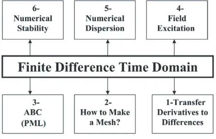
In this section, we investigate the mode splitting properties of the nanocavities resonators in a two-dimensional (2D) plasmonic waveguide with Ag-air-Ag interfaces using a finite-difference-time-domain (FDTD) method [17] and perfectly matched-layer (PML) as an absorbing boundary condition (ABC). In our numerical calculations with FDTD, the nanocavities resonators are described by a spatial discretization grid. A spatial grid size of Δx = Δy = 2 nm in the FDTD algorithm is found sufficient for convergence of the numerical results. Calculations in FDTD are performed according to the steps listed in Fig. 5 [27].
Figure 5. Layout of FDTD method.
Our system is made up of a 2D box (along the x- & y-axes) with propagation along the x-axis. UPML boundary conditions are applied at both boundaries iny andx of the box in order to eliminate the reflection of outgoing waves [27]. 200 nm width for the PML is found to be thick enough to fully absorb outgoing waves. The structure is supposed to be infinite along the z-direction. The equations of motion are solved with a time integration step Δt= (Δx/4c) = 1.7×10⁻³fs to avoid the problems of numerical dispersion and stability. The number of time steps is equal to 216, which is the necessary tested time for good convergence of the numerical calculations.
filtering effect should be observed in the waveguide-resonator system as shown in Fig. 2(a). As expected, the light is confined in the resonator when the wavelength equals 1.084µm, and the corresponding transmission dip of 0.3 can be achieved. This phenomenon can be clarified by the magnetic field distribution of the mode at wavelengths: 1.038, 1.158, and 1.084µm in Figs. 2(b), (c), (d). It is obvious from Figs. 2(b), (c) that the energy is highly coupled into the bus waveguide resulting in the weak magnetic distributions in the nanodisk. On the other hand, for Fig. 2(d) which represents the resonance of the nanodisk, the energy is highly coupled into the nanodisk resulting in weak magnetic distributions in the waveguide.
The second group of simulated results is presented in Fig. 6. The transmission spectrum of MIM plasmonic waveguide coupled with the two nanodisks is shown in Fig. 6(a). One can find that the transmission value at the resonance is very high compared to its counterpart results shown in Fig. 2(a). Simultaneously, two new transmission dips with wavelengths of 1.056 and 1.113µm are formed. The corresponding transmission dip of the splitmode transmission spectrum is near 0.4. In addition, the corresponding magnetic field distribution of several key wavelengths is shown in Figs. 6(b)–(d). The reason that the transmission is low atλ= 1.056 and 1.113µm is the destructive interference at waveguide between the electromagnetic energy coming from the first nanodisk which acts as a pump signal [28] and the electromagnetic energy propagating in the waveguide, as shown in Figs. 4(b), (c). By the same interpretation, for λ = 1.084µm which is also the resonance wavelength of the second nanodisk the destructive interference occur here at the first nanodisk between electromagnetic energy coupled from the second nanodisk which acts as a pump signal [28] and the electromagnetic energy coupled from the waveguide result in approximately no coupling between the waveguide and the two nanodisks.
(c) λ=1.113 μm (d) λ=1.084 μm (b) λ=1.056 μm (a)
Figure 6. (a) Transmission spectrum of the proposed structure in Figure 3 with R = 276 nm, g1 = 11 nm, g2 = 15 nm, (b)–(d) contour map of the magnitude of the magnetic field distribution for the structure.
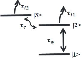
The above results and interpretations permit the use of the concept of three-level energy diagram system [28, 29] to unravel the physical origin of the mode splitting behavior. To do this, recall from [28, 29] the electromagnetically induced transparency EIT equation
Tab= 1−Ω21ΓΔ2 (ΓΔ)2+ 4
Δ2−Ω2242
(10)
EIT equation if we regard ω0δ→Δ, ω0(1/Qi1+ 1/Qw)→Γ, andω0/Qc →Ω2. Therefore, as shown in
Fig. 7, the incident waveguide is considered as the ground state|1. The first nanodisk coupled directly to the waveguide acts as a bright resonator with the radiative plasmonic state|2. The second nanodisk cannot be excited directly by the incident light and behaves as a dark resonator with the dark plasmonic state |3. The state |2 is coupled to the ground state |1 by a bright dipole-allowed transition with resonance frequency ω0. At the same time, it is coupled to a dark state |3, which might be detuned by a shift δ. The direct path |1–|3 is forbidden. The second nanodisk is excited only by near-field coupling with the first nanodisk corresponding to |2–|3 path. However, the coupling of the levels |2 and|3allows for a population of state|3, which will cause a back action and an excitation of level|2. According to the distributions of the magnetic fieldHy shown in Fig. 6(d), the realization of the mode
splitting response results from the strong destructive interference between two propagation pathways: the direct transition|1–|2 and the indirect one|1–|2–|3–|2.
Figure 7. Three-level model scheme of the plasmonic system.
As shown in Fig. 6(d), the filed in the nanodisk is extraordinarily suppressed due to the strong destructive interference. This destructive interference lets the first nanodisk act as a null with respect to the waveguide, and hence the SPP power is passed to the waveguide output, which is a direct evidence of the outstanding transmission window at the resonance wavelength. For the new transmission nulls, however, the first nanodisk is directly excited by the incident SPPs. For the second nanodisk excited from the first one, the coupling is enhanced at one null (in-phase coupling) and degrades at the other null (out-phase coupling). The in-phase coupling resonance occurs between the two nanodisks at λ= 1.056upmum (see Fig. 6(b)) whereas the out-phase coupling forms atλ= 1.113µm (see Fig. 6(c)). The incident SPP power can be coupled back into the waveguide by the first nanodisk, resulting in the newly appearing transmission nulls. Therefore, the presence of the second nanodisk can prevent the confinement and absorption of the SPP power which is absorbed previously by the first nanodisk resonance, thereby, achieve the novel mode splitting response.
4. THE TRANSMISSION CHARACTERISTICS WITH VARYING GEOMETRIC PARAMETERS
Figure 8. Transmission spectrum of the proposed structure with different R when g1 = 11 nm, g2= 15 nm.
Figure 9. Transmission spectrum of the proposed structure with different g2 when R = 276 nm, g1= 11 nm.
(a) (b) (c)
Figure 10. (a) Simulated transmission phase shift, (b) optical delay time and (c) group indices with R= 276 nm,g1 = 11 nm,g2= 15 nm.
variation characteristics of dip 1 and dip 2 with R indicates that this structure can be used in many different applications such as monitoring applications.
Figure 9 shows the transmission spectra of the proposed structure with different g2 when R = 276 nm,g1 = 11 nm. As we can see, the transmission dip 1 shifts to the long wavelengths; meanwhile, dips 2 shifts to short wavelengths wheng2 increases. The results of this figure can be easily interpreted as follows: the transmission spectrum tends to form one dip from the two dips with the increase of g2; the coupling between the two nanodisks decreases
an important index, and it can be described by the group indexng [30]
ng=
c vg
= c
Hτg = c H
dθ(ω)
dω (11)
where, vg and τg stand for the group velocity and the optical delay time in the selected structure,
respectively. c represents the speed of light. θ(ω) is the transmission phase shift and H the length from the light source to the detector. By means of detecting the transmission phase shift and a serial of calculations based on the above definitions of the group delay, we numerically investigate, with g1 = 11 nm, R = 276 nm, g2 = 15 nm, the optical group delay. Fig. 1 shows the transmitted phase shift (θ(ω)) between the waveguide input and output, group delay time (τg), and group index. It is
clear from Fig. 10(a) that the phase slope is negative and steepest around the resonance wavelengths of different modes. It can be seen from Fig. 10(b) that the optical delay is negative at resonance and positive at wavelengths of the split modes; fast-light occurs at resonance and slow light at wavelengths of the splitted modes.
5. CONCLUSION
In summary, a plasmonic coupling system consisting of MIM bus waveguide and two nanodisks as resonators is investigated both numerically and theoretically. The novel mode splitting effects with fast-light feature at resonance and slow-light feature at the splitting modes are realized respectively in the new structure. Such novel fast- and slow-light characteristics originate from the extreme destructive interference between the two nanodisks resonators. In this paper, the simulated results are verified by the CMT. This structure will open up a new opportunity to develop slow- and fast-light techniques and play a vital role in the integrated optical devices such as optical switching, monitoring, and optical storage.
REFERENCES
1. Ishizaka, Y., M. Nagai, T. Fujisawa, and K. Saitoh, “A photonic-plasmonic mode converter using mode-coupling-based polarization rotation for metal-inserted silicon platform,”IEICE Electronics Express, Vol. 14, No. 2, 1–10, 2017.
2. Maier, S., Plasmonics: Fundamentals and Applications, 2007.
3. Namin, F. A., Y. A. Yuwen, L. Liu, A. H. Panaretos, D. H. Werner, and T. S. Mayer, “Efficient design, accurate fabrication and effective characterization of plasmonic quasi-crystalline arrays of nano-spherical particles,” Sci. Rep., Vol. 6, 22009, 2016.
4. Polyakov, A., M. Zolotorev, P. J. Schuck, and H. A. Padmore, “Collective behavior of impedance matched plasmonic nanocavities,”Opt. Express, Vol. 20, No. 7, 7685–7693, 2012.
5. Guo, L. and Z. Sun, “Cooperative optical trapping in asymmetric plasmon nanocavity arrays,”
Opt. Express, Vol. 23, No. 24, 31324–31333, 2015.
6. Cano, D., M. L. Nesterov, A. I. Fernandez-Do-minguez, F. J. Garcia-Vidal, L. Martin-Moreno, and E. Martin-Moreno, “Domino plasmons for subwavelength terahertz circuitry,”Opt. Express, Vol. 18, No. 1, 754–764, 2010.
7. Janipour, M., M. Karami, R. Sofiani, and F. Kashani, “A novel adjustable plasmonic filter realization by split mode ring resonators,” Journal of Electromagnetic Analysis and Applications, Vol. 5, No. 12, 405–414, 2013.
8. Noual, A., A. Akjouj, Y. Pennec, J.-N. Gillet, and B. Djafari-Rouhani, “Modeling of two-dimensional nanoscale Y-bent plasmonic waveguides with cavities for demultiplexing of the telecommunication wavelengths,” New Journal of Physics, Vol. 11, 103020, 2009.
9. Willingham, B. and S. Link, “Energy transport in metal nanoparticle chains via sub-radiant plasmon modes,” Opt. Express, Vol. 19, 6450–6461, 2011.
Nanomaterials, Vol. 2013, 2013.
14. Amir, S., S. R. Mirnaziry, and M. S. Abrishamian, “Numerical investigation of tunable band-pass/band-stop plasmonic filters with hollow-core circular ring resonator,” Journal of the Optical Society of Korea, Vol. 15, No. 1, 82–89, 2011.
15. Amirreza, M., et al., “Plasmonic coaxial waveguide-cavity devices,”Optics Express, Vol. 23, No. 16, 20549–20562, 2015.
16. John, D., G. Steven, N. Joshua, and D. Robert,Photonic Crystals: Molding the Flow of Light, 2nd Edition, Princeton University Press, 2008.
17. Taflove, A. and S. C. Hagness,Computational Electrodynamics: The Finite Difference Time-domain Method, Artech House, Boston, 2005.
18. El Mashade, M. B. and M. N. Abdel Aleem, “Analysis of ultra-short pulse propagation in nonlinear optical fiber,”Progress In Electromagnetics Research B, Vol. 12, 219–241, 2009.
19. Tian, J., R. Yang, and L. Song, “Optical properties of a Y-splitter based on hybrid multilayer plasmonic waveguide,”IEEE Journal of Quantum Electronics, Vol. 50, No. 11, 898–903, 2014. 20. Dong, H. M., et al., “Plasmonic splitter based on the metal-insulator-metal waveguide with periodic
grooves,” Optics Communications, Vol. 283, No. 9, 1784–1787, 2010.
21. Pannipitiya, A., et al., “Improved transmission model for metal-dielectric-metal plasmonic waveguides with stub structure,”Optics Express, Vol. 18, No. 6, 6191–6204, 2010.
22. Joannopoulos, J. D., S. G. Johnson, J. N. Winn, and R. D. Meade, Photonic Crystals: Molding the Flow of Light, 2nd Edition, Princeton University Press, Princeton, 2008.
23. Zhan, G., et al., “Asymmetric band-pass plasmonic nanodisk filter with mode inhibition and spectrally splitting capabilities,” Optics Express, Vol. 22, No. 8, 9912–9919, 2014.
24. Noual, A., et al., “Modeling of two-dimensional nanoscale Y-bent plasmonic waveguides with cavities for demultiplexing of the telecommunication wavelengths,”New Journal of Physics, Vol. 11, No. 10, 103020, 2009.
25. Bozhevolnyi, S. I., “Plasmonic nano-guides and circuits,”Frontiers in Optics, 2008.
26. Manolatou, C., M. J. Khan, S. Fan, P. R. Villeneuve, H. A. Haus, and J. D. Joannopoulos, “Coupling of modes analysis of resonance channel add-drop filters,” IEEE J. Quantum Electron., Vol. 35, 1322–1331, 1999.
27. Nady, M., “Modeling of ultra-short pulse propagation in nonlinear optical fibers,” master thesis, Al-AZHAR University, Faculty of Engineering, Dept. of Electronics and Electrical communications, 2009.
28. Li, Y. Q. and M. Xiao, “Observation of quantum interference between dressed states in an electromagnetically induced transparency,”Physical Review A, Vol. 51, No. 6, 4959, 1995.
29. Xing, Z., et al., “Plasmonically induced absorption and transparency based on stub waveguide with nanodisk and Fabry-Perot resonator,”Plasmonics, 1–8, 2016.
30. Wang, J., et al., “A novel planar metamaterial design for electromagnetically induced transparency and slow light,”Optics Express, Vol. 21, No. 21, 25159–25166, 2013.