Analysis of Clock Gating Applications for Energy
Efficient Implementations on FPGA’s
S Uday Venkat Kiran G Goutham Kumar B Priyadharshini Asst. Prof. H.O.D PG Student Nigama Engineering College Nigama Engineering College IARE
[email protected] [email protected] [email protected]
ABSTRACT: This paper investigates the reduction of dynamic
power for streaming applications yielded by asynchronous dataflow designs by using clock gating techniques. Streaming applications constitute a very broad class of computing algorithms in areas such as signal processing, digital media coding, cryptography, video analytics, network routing, packet processing, etc. This paper introduces a set of techniques that, considering the dynamic streaming behavior of algorithms, can achieve power savings by selectively switching off parts of the circuits when they are temporarily inactive. The techniques being independent from the semantic of the application can be applied to any application and can be integrated into the synthesis stage of a high-level dataflow design flow. Experimental results of at-size applications synthesized on field-programmable gate arrays platforms demonstrate power reductions achievable with no loss in data throughput.
Index Terms: Clock-gating, dataflow, high-level synthesis
INTRODUCTION
Power dissipation is currently the major limitation of silicon computing devices. Reducing power has also other beneficial effects, it implies less stringent needs for cooling, improved longevity, longer autonomy in the case of battery operated devices and obviously, lower power costs. For all these reasons power also frequently affects the choice of the computing platform right at the outset. For example, field-programmable gate arrays (FPGAs) imply higher power dissipation per logic unit when compared to equivalent application-specific integrated circuit (ASIC), but often compare favorably to conventional processors used for the same functional tasks.
For any silicon device, power dissipation can be partitioned into two components: 1) a static and 2) a dynamic component. Static power dissipation also referred to as quiescent or standby power consumption is the result of the leakage current of the transistors, also affected by the ambient temperature. By contrast, dynamic power dissipation is caused by transistors being switched and by losses of charges being moved along wires. Power dissipation increases linearly with frequency, largely due to the influence of parasitic capacitances. To counteract this effect, ASIC designers have employed clock gating (CG) techniques in the last 20 years.
Different strategies for optimizing power consumption on ASICs and FPGAs are discussed in Section II. These papers describe the impact of a chosen technology for a given architecture, but do not describe how to reduce power at the design abstraction level. As a consequence, adding power controllers at the behavioral description design stage constitutes an additional task that has to be carried-out with care to avoid introducing undesired application behaviors and
might reduce the portability of the code (i.e., platform is changed during the development process). In addition, it is extremely difficult for HLSs approaches that are based on imperative model of computations (MoCs).
To apply power optimization solutions that can be yielded by automatic tools starting from the (imperative) behavioral description. Conversely, dynamic dataflow designs such as for instance the ones expressible using the formal RVC-CAL language possess interesting properties that can be exploited for reducing the power consumption without affecting, by construction, the behavioral characteristics of the application. In RVC-CAL, every actor can concurrently execute processing tasks, executions might be disabled by input blocking reads, and every communications among actors can occur only by means of order preserving lossless queues. As a consequence, an actor may be stopped for a certain period if its processing tasks are idle or its outputs queues (buffers) are full with-out impacting the overall throughput and semantically behavior of the design. In addition, to higher levels of dynamic behaviors that might be present in a given dataflow design, correspond higher levels of power reduction opportunities. This is not the case for synchronous dataflow designs that always consume and produce a fixed amount of data tokens. Thus, synchronous dataflow design always dissipates a constant amount of power compared to asynchronous dataflow. In this perspective, the techniques that transform intrinsically dynamic algorithm into static versions such as the ones that are implemented by static dataflow MoC for deriving analytical guaranteed bounds or other analyzability purposes. In general, this transformation is done by introducing dummy tokens guaranteeing constant rates. Thus, in terms of power optimization such approaches are inefficient.
This paper is organized as follows. In Section II, previous works on CG are briefly introduced. Section III describes in detail the CG strategy and how it is applied on a dataflow design. In Section IV, experimental results are presented and conclusions are finally drawn in Section V.
RELATED WORK
Available online: https://edupediapublications.org/journals/index.php/IJR/ P a g e | 10
CLOCK-GATING STRATEGY
Current FPGA families support different CG strategies and each manufacturer provides its own IP for managing these different approaches. The methodology described here is based on using primitives specific to Xilinx FPGA architectures. However, this methodology can be modified to support other FPGA vendor’s primitives. In the remainder of this section, it is briefly described how CG techniques are implemented on Xilinx FPGAs and how an automatic CG strategy within Xronos HLS is realized.
A. Profile Guided Buffer Size
The execution of a dataflow program consists of a sequence of action firings. These firings can be correlated to each other in a graph-based representation using an approach called execution trace graphing (ETG). The graph is an acyclic directed graph where each node represents an action firing, and a directed arc represents either a data or a control dependency between two different action firings. The effectiveness of analyzing a dataflow program using an ETG is demonstrated. Xronos provides profiling for each firing execution in clock cycles. This is achieved by retrieving the difference of DONE and GO signals for each action firing during register-transfer level simulation. Timing information is added to the ETG for each firing and each dependency arises according to a corresponding time value, thus transforming the ETG into a weighted graph. A close-to-optimal buffer size configuration, in terms of execution throughput and buffer memory utilization, can be obtained through an iterative analysis of the algorithmic critical path evaluated using the weighted ETG.
B. Coarse-Grained Clock Gating Strategy
When the output buffer of any actor is full, the clock of this actor should be turned off as the actor is idle. This is because switching off its clock will not have an impact on design throughput. Even though RVC-CAL dataflow designs are used for the behavioral description, such CG strategy is more general and can be applied to systems that represent the execution of a process that communicates with asynchronous FIFO buffers. The queues should be asynchronous for lossless communication when an actor is clock gated and a design has differing input clock domains.
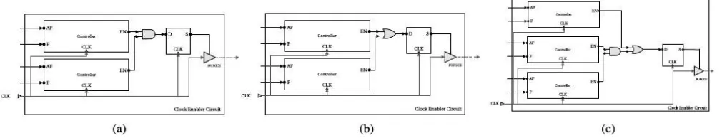
This strategy consists of adding a clock enabler circuit for activating the actors’ clock. This circuit contains: a controller for each output port queue of each actor, a combinatorial logic for the con-figuration of the output ports, and a clock buffer (which enables the clock). A representation of an actor with a single output port being clock gated is illustrated in Fig. 1. As depicted, queues are asynchronous. Queues have two input clocks: one for consuming tokens and one for producing them. Additionally, queues have two output ports: 1) AF for almost full and 2) F for full. The actors input clock is connected to the output of the clock enabler circuit. Finally, the clock buffer BUFGCE input clock should be connected with a flip-flop for glitch-free CG.
The flip-flop will introduce one-clock latency when the clock is switched off, but this additional clock cycle will not have an impact on actors that are on the critical path. Those actors are not being clock gated because the TURNUS dimensioning of the FIFO queues is based on critical path analysis. Hence, this approach does not impact overall performance.
Fig 1 CG methodology applied for actor A. The actor A has two outputs one of those have a fan-out of two. The clock enabling circuit takes the Almost Full and Full signal of each queue and a clock from a clock domain and as a result it is going to activate or deactivate the clock of actor A.
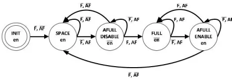
Fig 2 State machine of the clock enabling controller, the controller has two inputs, F for full, AF for almost full and one output en as the enable signal.
1) Clock Enabling Controller: The clock enabling controller is represented in Fig. 2. The controller is implemented as a finite state machine (FSM) having a clock; a reset; input F, for full; input AF, for almost full; and output EN, for enable. The AF input becomes active high when there is only one space left on its FIFO Queue. Its
FSM has five states S = {INIT, SPACE, AFULL_DISABLE, FULL, AFULL_ENABLE} The controller starts with the INIT state and maintains the EN output port at active high until F and AF become active low. The active high EN is maintained during the SPACE state. As a queue becomes full, the state changes to AFULL_DISABLE. In this state, the EN output passes to an active low. A conservative approach is taken in this state as the BUFGCE disables the output clock on the high-to-low edge. The clock enables entering the BUFGCE should be synchronized to the input clock. Once the queue becomes full, the controller maintains the EN at active low. When a token is consumed from the queue, the controller passes to the A FULL_ENABLE state, and it activates the clock then, depending on whether the buffer becomes full or almost full, the state changes to either the FULL or the SPACE state.
Fig 3 Clock enabler circuit in three different configurations (a) Single output port with a fan-out, (b) Two different output ports. (c) Single output port with a fan-out and another output port.
These situations are detected and generated automatically as described in the “always clause.” A flip-flop (created by the always clause) is connected between the BUFGCE and the final OR (or) AND port. Thus, clock glitches are eliminated and the clock enabling is runt free. The last output of the CG is a new clock that is connected to the actors, its fan outs, and its queues’ write and read clocks (CLK W and CLK R, respectively) as visualized in Fig. 1.
EXPERIMENTAL RESULTS
In this section, the power reduction gain of the aforementioned methodology is evaluated by applying it to a video decoder design. In the reader can find a variety of RVC-CAL applications for dataflow programs. One of these applications is the intra MPEG-4 simple profile decoder. Due to restrictions on the number of clock buffers in Xilinx FPGAs, the design selected was refectories to result in 32 actors.
A. Test Design
The intra MPEG-4 SP description contains 32 actors and it is 4:2 decoders which are separated into eight processing blocks: four components for luminance (Y) and two each for chrominance (U and V). The parser block includes the syntactical bit stream parser and the variable length decoding process which the Tex Y, U, and V blocks (for texture) implements. The residual decoding (ac-dc pre-diction, inverse scanning, inverse quantization, and IDCT) and the MOT Y, U, and V realize the motion compensation stage (frame-buffer, interpolation, and residual error addition). Due to the nature of the experiments, the motion compensation blocks contain only the residual error addition actor. By using the TURNUS profiler, a close to minimum queue size for each queue in the decoder is determined.
TABLE I
SYNTHESIS RESULTS OF THE INTRA MPEG-4 SIMPLE PROFILE DECODER
SYNTHESIZED FOR VIRTEX 7 XC7VX485T-2 FPGA, WITH AND WITHOUT
CG
B. Experimental Flow
For the experimental evaluation, a Virtex 7 XC7VX485T-2 FPGA (VC707 Evaluation Kit) was used. The HDL code of the decoder was generated by Xronos and synthesized with the Xilinx XST synthesizer. Following synthesis, placing and routing was applied to produce a final net list. This net list was then simulated with Modelsim to extract the switching activity information (SAIF file) of the design. The Xilinx XPower analyzer was then used to determine power consumption, using the design net list, the design constraints, and the simulation activity SAIF as inputs. Also, all of the results given have a high confidence level meaning that at least 97% of the design nets are found within the SAIF file. Table I shows the synthesis results of the intra MPEG-4 simple profile decoder with and without CG. This example demonstrates that the clock gated decoder uses more slices than the no clock gated one. Even though this represents 28% more slices overall compared to the no clock gated decoder, the CG methodology requires only 15% more LUTs. A 50 MHz clock has been given as a synthesis constraint.
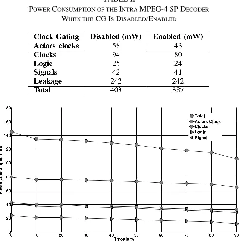
Table II depicts the power consumption of the decoder including the circuit of the CG methodology. Two test cases were considered: 1) CG deactivated and 2) CG activated when decoding at maximum throughput.
Table II, the actor’s clocks label only the power consumption of the clock nets of the actor. The clocks cell contains the actors clock nets, the enabling of clock buffer nets, and the nominal 50 MHz clock net. As a result of CG, the actor’s clocks consume 26% less power, but due to the decoder running at full speed, the activation rate of the logic and signals nets remain resulting in a total power decrease of 4% (16mW less).
C. Power Saving Efficiency over Decoder Throttling
As described in Table I the maximum decoder throughput rate is 350frames/s for a QCIF image (176×144 pixels). For the experiment, the decoder is throttled such that it decodes only 30 images per second for two resolutions QCIF and CIF (384×288 pixels).
TABLE II
POWER CONSUMPTION OF THE INTRA MPEG-4 SP DECODER
WHEN THE CG IS DISABLED/ENABLED
Fig 4 Power consumption of overall clocks, the signals, logic, and the total dynamic power consumption of the intra MPEG-4 SP decoder when its output is throttled from 0% to 90%.
D. Power Saving Efficiency over Bandwidth Demand
In this experiment, the decoder was throttled from 0% to 90% simulating a channel with differing consumption rates. This is an example of CG applied not specifically to video decoding applications, but to a general application. Fig. 4 represents the power consumption of the decoder when its output is throttled from 0% to 90%. As demonstrated, the total dynamic power consumption has decreased from 145mW to 106mW, a power reduction of 27%. Compared to the non clock gate decoder, the dynamic power has been reduced by 34%. Fig. 5 reports the power consumption of each clock and their activation rate when throttled. From this graph, the data of 15 actors has been removed due to their activation rate being more than 99%. All actor clock activation rates decreased while increasing throttle (apart from two cases, par_splitter_Qp_clk and tex_Y_DCR_addr_clk where the power consumption increased slightly). The decoder used was YUV 420. When it reaches 60%, the decoder throttles the luminance decoding, but the chrominance decoding remains active. This also occurred during a behavioral simulation in Modelsim.
Fig. 5 Power consumption and activation rate of each clock gated actor clock of the MPEG-4 SP decoder. Median values were retrieved from an MPEG-4 reference QCIF input stimuli (video sequence). (a) Actors clock power consumption. (b) Actors clock activation rate.
V CONCLUSION
REFERENCES
[1] M. Pedram, “Power minimization in IC design: Principles and applications,” ACM Trans. Design Autom. Electron. Syst., vol. 1, no. 1, pp. 3–56, Jan. 1996. [Online]. Available:
http://doi.acm.org/10.1145/225871.225877
[2] Q. Wu, M. Pedram, and X. Wu, “Clock-gating and its appli-cation to low power design of sequential circuits,” IEEE Trans. Circuits Syst. I, Fundam. Theory Appl., vol. 47, no. 3, pp. 415–420, Mar. 2000.
[3] G. E. Tellez, A. Farrahi, and M. Sarrafzadeh, “Activity-driven clock design for low power circuits,” in IEEE/ACM Int. Conf. Comput.-Aided Design Dig. Tech. Papers (ICCAD), San Jose, CA, USA, Nov. 1995, pp. 62–65.
[4] E. A. Lee and A. Sangiovanni-Vincentelli, “Comparing models of com-putation,” in Proc. IEEE/ACM Int. Conf. Comput.-Aided Design, Austin, TX, USA, 1997, pp. 234–241.
[5] G. Kahn, “The semantics of simple language for parallel programming,” in Proc. IFIP Congr., Stockholm, Sweden, 1974, pp. 471–475. [6] E. A. Lee and D. G. Messerschmitt, “Static scheduling of synchronous
data flow programs for digital signal processing,” IEEE Trans. Comput., vol. 36, no. 1, pp. 24–35, Jan. 1987.
[7] E. A. Lee and T. M. Parks, “Dataflow process networks,” Proc. IEEE, vol. 83, no. 5, pp. 773–801, May 1995.
[8] S. Suhaib, D. Mathaikutty, and S. Shukla, “Dataflow architectures for GALS,” Electron. Notes Theor. Comput. Sci., vol. 200, no. 1, pp. 33– 50, 2008.
[9] T.-Y. Wuu and S. B. K. Vrudhula, “Synthesis of asynchronous systems from data flow specification,” Inf. Sci. Inst., Univ. Southern California, Los Angeles, CA, USA, Tech. Rep. ISI/RR-93-366, Dec. 1993. [10] B. Ghavami and H. Pedram, “High performance asynchronous design
flow using a novel static performance analysis method,” Comput. Elect. Eng., vol. 35, no. 6, pp. 920–941, Nov. 2009.
[11] S. C. Brunet et al., “Partitioning and optimization of high level stream applications for multi clock domain architectures,” in Proc. IEEE Workshop Signal Process. Syst. (SiPS), Taipei, Taiwan, Oct. 2013, pp.177–182.
[12] S. Casale-Brunet, “Analysis and optimization of dynamic dataflow pro-grams,” Ph.D. dissertation, STI Elect. Eng., STI, Lausanne, Switzerland, 2015.
[13] E. Bezati, “High-level synthesis of dataflow programs for heterogeneous platforms,” Ph.D. dissertation, STI, Lausanne, Switzerland, 2015.
[14] S. Casale-Brunet, M. Mattavelli, and J. W. Janneck, “Buffer optimiza-tion based on critical path analysis of a dataflow program design,” in Proc. IEEE Int. Symp. Circuits Syst. (ISCAS), Beijing, China, May 2013,
pp.1384–1387.
[15] Analysis of Power Savings from Intelligent Clock Gating, Xilinx, San Jose, CA, USA, Aug. 2012.
[16] (2014). Open RVC-CAL Applications. Accessed on Feb. 25, 2014. [Online]. Available: http://github.com/orcc/orc-apps