IJEDR1604022
International Journal of Engineering Development and Research (www.ijedr.org)120
________________________________________________________________________________________________________
Abstract - As we are approaching the limits of scaling, Scaling down the thickness of gate oxide is not found to be a good idea, as it causes a reduction in ON–OFF current ratio though S/S remains mostly unaffected. so we propose the impact of variation in design parameters, such as spacer length and spacer material type, gate dielectric and its thickness, and integrate distance on the device performance of a DG spacer-based silicon nanowire ambipolar FET (SiNWFET),has been carried out for the first time. The design of spacer-based potentially improved reconfigurable FET devices for future low-power CMOS applications. It reports various optimization aspects of an ambipolar silicon nanowire field-effect transistor with high-κ source–drain (S/D) spacer using coupled 3-D Technology.
Keywords - SiNWFET, Spacer, ambipolarity, variability, high- k.
________________________________________________________________________________________________________
I. INTRODUCTION
As we are approaching the limits of scaling for new devices is becoming indispensible for continuing the performance gains. Silicon nanowire-based field-effect transistors are considered as an ideal replacement to planar as well as fin-
Shaped field-effect transistors for future low-dimensional electronics [2]-[4].
Many of their keynote advantages as compared with bulk device topologies are reduced short-channel effects (SCEs) and higher ON–OFF current ratio under similar biasing arrangements [5-6]. They have also proven their usefulness inbiosensing, logic computation, and other high-frequency-based applications. The high input impedance and low output impedance and low noise level make FET for superior of the bipolar transistor.
In transistor family we are having the many advantages but along with that we are having some drawbacks. So that we move to the another type of transistor called Field effect transistor (FET) In normal FETs we have many advantages like high input impedance of several mega ohms. The noise produced by a FET is less than that produced by a BJT but they have the smaller gain bandwidth product compare with the other transistors. Carbon nanotube field-effect transistors showing different transistor characteristics due to a change resulting from Schottky barrier modulation at the contacts to bulk have been demonstrated in [8], and the equivalent circuit model for Schottky barrier at metal/semiconductor junction for a carbon nanotube is discussed in [9]. For the last few years, programmable nanowire field-effect transistors relying on the proper tuning of Schottky barriers have been a topic of intense research [10]–[12] because of their added advantage over conventional CMOS devices, which have static electrical characteristics. Being fully compatible with the conventional CMOS process flow [13]. A triple metal double gate (TM-DG) MOSFET with high-k dielectrics has been proposed to overcome the short channel effects. The metal gates have been used to remove the poly silicon depletion of conventional double gate (DG) MOSFET due to aggressive scaling to sub 100 nm regimes. It has been observed that use of metal gate with different work functions along with high-k dielectric improves the carrier transport in the channel [14]. A modified structure of TFET incorporating ferroelectric oxide as the complementary gate dielectric operating in negative capacitance zone, called the Negative Capacitance Tunnel FET (NCTFET). The proposed device effectively combines two different mechanisms of lowering the sub threshold swing (SS) for a transistor garnering a further lowered one compared to conventional TFET [6]. In [20], we have demonstrated a novel approach to improve the performance of a dual-gate (DG) ambipolar FET with the help of source–drain (S/D) spacer engineering. It has been observed that the device under study shows superior electrical characteristics like improved current drive and lower Sub threshold swing (S/S). In this paper, we observe the impact of variation of critical design parameters, such as spacer length (LSP) and thickness
(tSP), dielectric constant of spacer material (κSP), gate oxide thickness (tox) and intergate separation (dG1G2) on device
performance. Our simulation results show that though high-κ spacer improves device performance like ION , S/S.
In section 1 we discuss the overall design metrics like literature, In Section II, deals with Si nanowire device structure as well as highlight the 3-D simulation methodology used. SectionIII summarizes all the obtained results. Finally Section IV deals with conclusion and future scope of the paper.
IJEDR1604022
International Journal of Engineering Development and Research (www.ijedr.org)121
Fig: 1. 3-D isometric viewThis is the basic silicon nanowire based field effect transistor in 3-D form. The proposed structure have the silicon nanowire of length 680nm, around with that nanowire we are using the Rutile phase TiO2 Gate dielectric of thickness 10 nm, which is used as a replacement of SiO2 for better off state performance. Due to the use of gate dielectric as TiO2 it increases the
electron density as 1.5*1020 cm-3 with HfO
2 and 2.2*1020 cm-3 with SiO2. NiSi2 is employed at source and drain periphery forming
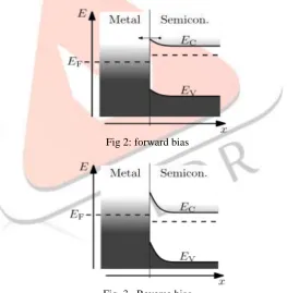
schottky contacts. Metal and semiconductor combine and form the junction, that junction can either rectifying or non-rectifying. The rectifying M-S junction forms a schottky barrier. Making device known as schottky diode and non- rectifying is called as ohmic contact. Schottky diode has higher current density than an ordinary P-N junction. The most important difference between the p-n diode and the Schottky diode is the reverse recovery time (trr), when the diode switches from the conducting to the
non-conducting state. In a p–n diode, the reverse recovery time can be in the order of hundreds of nanoseconds to less than 100 ns for fast diodes. Schottky diodes do not have a recovery time. Not all metal–semiconductor junctions form a rectifying Schottky barrier, a metal–semiconductor junction that conducts current in both directions without rectification. The forward and reverse biased schottky diode is shown in below figure.
Fig 2: forward bias
Fig. 3. Reverse bias
A small gap of 5 nm is kept between outer gate edge and NiSi2/Si Schottky contact to incorporate HfO2 Spacer (Lsp = 2 nm and tsp = 10 nm) on both S/D ends. To model the impact of air Spacer in the TCAD simulations and correctly describe the interaction between gate and Schottky contact, a low-κ spacer is placed in between the high-κ spacer and S/D electrodes. This spacer arrangement in our structure is shown in fig.4
IJEDR1604022
International Journal of Engineering Development and Research (www.ijedr.org)122
structures.III. SIMULATION RESULTS
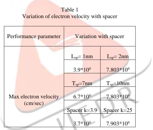
A. Effects of Variation in the Spacer Length (Lsp):
In our design we use the spacer length as 2 nm and then we observe the structure but those figures are not obtained in regular usage software so we only use the comparison table with various spacer This accounts to the parasitic injection of electrons at drain contact at higher Lsp. Table I shows the 2-D electron velocity comparison in the silicon nanowire core at VG1 = 3 V, VG2 = 1.5 V, and VDS = 0.8 V, as a function of spacer length, thickness, and spacer material type. With increase in Lsp from 1 to 2 nm. The device displays 50.01% higher carrier velocity which relates to improved electrostatic coupling near the Schottky junction
At higher spacer lengths.
Table 1
Variation of electron velocity with spacer
Performance parameter Variation with spacer
Max electron velocity (cm/sec)
Lsp= 1nm Lsp= 2nm
3.9*106 7.803*106
Tsp=7nm Tsp=10nm
6.7*106 7.803*106
Spacer k=3.9 Spacer k=25 3.7*106 7.903*106
It is observed that the use of a high-k dielectric as a spacer brings an improvement in the OFF-state current by more than one order of magnitude thereby making the device more scalable. However, the ON-state current is only marginally affected by increasing dielectric constant of spacer. The effects of spacer width (Wsp) on device performance are also studied. ON-state current marginally decreases with spacer width. Similar observations can also be seen when Spacer Width is changed from 7 to 10 nm, though the improvement obtained in peak velocity is only 13.04%. This shows that coupling does not increase significantly with increase in spacer Width mainly because of the physical distance and lesser impact of tsp on outer fringe lines. Finally, ∼72% increase in Vmax with the inclusion of high-κ (HfO2) spacer relates to a significant rise in the concentration of the fringing electric field near the NiSi2/Si Schottky contact.
B. Effects of Variation in Dielectric Constant of Gate Oxide:
We observe the device performance comparison for various gate dielectrics in fig 5. The Equivalent oxide thickness in each case is fixed to 0.67 nm, and different cases are considered for comparison as TiO2 (k=60)and SiO2 (k=3.9) With TiO2 gate
oxide, the peak electron density increases by 1.5 × 1020 cm-3 and 2.2 × 1020 cm-3 at a distance of 0.19 μm from the source
electrode as compared with the SiO2. when there is an enhancement in the internal fringe field due to a higher κ value of gate
IJEDR1604022
International Journal of Engineering Development and Research (www.ijedr.org)123
(a)(b)
Fig. 5. Impact of TiO2 as gate dielectric on (a) Electron density, (b) electrostatic potential.
In above fig by varying the distance of the spacer we get different values of potential, density. those are also observed for different spacers.
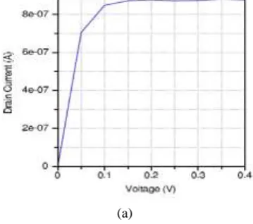
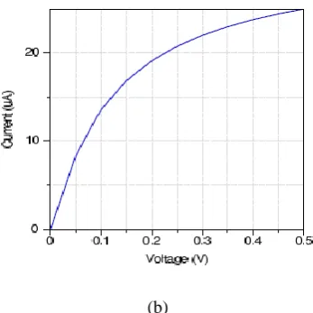
Variation of on current in proposed design:
By using the spacer of HfO2 and TiO2 we may get the some variations as that schottky contacts form a junction in the
device due to that we can get the current values of on current those are useful to get the on-off current ratio. This Ion/Ioff ratio increases by increasing the on current, and by decreasing the off current with the usage of schottky contact.
The fig .6 shows the variation of current with different voltages. For a small value of voltage variation also get large variation in the current. Here we observe the on current and drain current of the structure shown below.
IJEDR1604022
International Journal of Engineering Development and Research (www.ijedr.org)124
(b)Fig 6: (a) voltage vs. on current (b) voltage Vs drain current Related parameters variations:
In our structure we are using the spacer and silicon nanowire due to these we get more effective observations then the existed techniques. It is found to degrade by 11.7 and 78.9 ps with scaling of intergate distance in case of nFET for HfO2 and SiO2 spacers, respectively. However, in the case of pFET, the effect of rise in coupling capacitance is actually offset by a substantial increase in drive current for which the delay (τd ) is found to increase by 47.4 and 77.7 ps for HfO2 and SiO2 spacers, respectively, at higher dG1G2 . we observe the variation of electric energy with the transmission coefficient .in our design we observe that our spacer is more comfortable then other spacers , we also observe with different spacers the variation in the on-off current ratio of our design below table 2 shows the different parameter varies with different spacers among those TiO2 is more
advantageous spacer than other compounds due to its high dielectric value.
Table 2 Variation in device performance with different spacer materials Spacer material Ioff nFET
(x10-17A)
Ion nFET
(x10-6)
Ion / Ioff
(x1011)
SiO2 1.18 0.829 0.702
Si3N4 0.478 1.29 2.69
HfO2 2.16 2.13 0.986
TiO2 4.89 2.7 0.552
IV. CONCLUSION AND FUTURESCOPE
This paper shows a novel concept to improve the performance of a dual gate ambipolar FET architecture using high-κ S/D spacers. Extensive benchmarking with the existing reconfigurable device topologies shows that the proposed device exhibits improved electrical characteristics like higher ION/IOFF and lower S/S along with substantial reduction in sub threshold leakage current, which makes it perfectly suitable for low power digital design. the proposed device shows very low OFF-current, which makes advantageous for energy-efficient low-power applications. Apart from this, significant improvements in terms of ION and S/S are also obtained as compared to previously reported ambipolar devices based on silicon. It is worth mentioning that all the above mentioned performance gains are obtained at scaled supply voltage than those reported earlier. Our structure can further implemented for design of spacer-based potentially improved reconfigurable FET devices for future low-power CMOS applications.
V. REFERENCES
[1].Abhishek Bhattacharjee, Graduate Student Member, IEEE, and Sudeb asgupta,Member,IEEE, “Optimization of Design Parameters in Dual-κ Spacer-Based Nanoscale Reconfigurable FET for Improved Performance,” IEEE Trans. Electron Devices,vol.63,no.3,march 2016.
[2]. K. Nayak, M. Bajaj, A. Konar, P. J. Oldiges, K. Natori, H. Iwai, K. V. R. M. Murali, and V. R. Rao, “CMOS logic device and circuit performance of Si gate all around nanowire MOSFET,” IEEE Trans. Electron Devices, vol. 61, no. 9, pp. 3066–3074, Sep. 2014.
[3] Y. Cui, Z. Zhong, D. Wang, W. U. Wang, and C. M. Lieber, “High performance silicon nanowire field effect transistors,” Nano Lett., vol. 3, no. 2, pp. 149–152, 2003.
IJEDR1604022
International Journal of Engineering Development and Research (www.ijedr.org)125
[5] .A. Majumdar, S. Bangsaruntip, G. M. Cohen, L. M. Gignac, M. Guillorn, M. M. Frank, J. W. Sleight, and D. A. Antoniadis, “Room-temperature carrier transport in high-performance short-channel silicon nanowire MOSFETs,” in IEDM Tech. Dig., Dec. 2012.[6]. B. Yu, Y. Yuan, P. M. Asbeck, and Y. Taur, “Scaling of nanowire transistors,” IEEE Trans. Electron Devices, vol. 55, no. 11, pp. 2846–2858, Nov. 2008.
[7] J.-H. Ahn, S.-J. Choi, J.-W. Han, T. J. Park, S. Y. Lee, and Y.-K. Choi, “Double-gate nanowire field effect transistor for a biosensor,” Nano Lett., vol. 10, no. 8, pp. 2934–2938, Jul. 2010.
[8] S. J. Wind, J. Appenzeller, and P. Avouris, “Lateral scaling in carbonnanotube field-effect transistors,” Phys. Rev. Lett., vol. 91, no. 5, pp. 058301-1–058301-4, Jul. 2003.
[9] T. Yamada, “Equivalent circuit model for carbon nanotube Schottky barrier: Influence of neutral polarized gas molecules,” Appl. Phys. Lett., vol. 88, no. 8, pp. 083106-1–083106-3, 2006.
[10] M. De. Marchi, D. Sacchetto, S. Frache, J. Zhang, P.-E. Gaillardon,Y. Leblebici, and G. De Micheli, “Polarity control in double-gate, gateall- around vertically stacked silicon nanowire FETs,” in IEDM Tech. Dig., Dec. 2012.
[11] A. Heinzig, S. Slesazeck, F. Kreupl, T. Mikolajick, and W. M. Weber, “Reconfigurable silicon nanowire transistors,”vol. 12, no. 1, 2012.
[12] J. Zhang, X. Tang, P.-E. Gaillardon, and G. De Micheli, “Configurable circuits featuring dual-threshold-voltage design with three-independentgate silicon nanowire FETs,” IEEE Trans. Circuits Syst. I, Reg. Papers, vol. 61, no. 10, pp. 2851–2861, Oct. 2014.
[13] A. Heinzig, T. Mikolajick, J. Trommer, D. Grimm, and W. M. Weber, “Dually active silicon nanowire transistors and circuits with equal electron and hole transport,” Nano Lett., vol. 13, no. 9, pp. 4176–4181, Aug. 2013.
[14] Y. Jiang, T. Y. Liow, N. Singh, L. H. Tan, G. Q. Lo, D. S. H. Chan, and D. L. Kwong, “Nanowire FETs for low power CMOS applications featuring novel gate-all-around single metal FUSI gates with dual _m and VT tune-ability,” in IEDM Tech. Dig., Dec. 2008.
[15] M. Mongillo, P. Spathis, G. Katsaros, P. Gentile, and S. De Franceschi, “Multifunctional devices and logic gates with undoped silicon nanowires,” Nano Lett., vol. 12, no. 6, pp. 3074–3079,May 2012.
[16] J. Trommer, A. Heinzig, S. Slesazeck, T. Mikolajick, and W. M. Weber, Elementary aspects for circuit implementation of reconfigurable nanowire transistors,” IEEE Electron Device Lett., vol. 35, no. 1,Jan. 2014.
[17].M. Kadoshima et al., “Rutile-type TiO2 thin film for high-k gate insulator,” Thin Solid Films, vol. 424, no. 2, pp. 224–228, Jan. 2003.
[18] J. Zhang, M. De Marchi, D. Sacchetto, P.-E. Gaillardon, Y. Leblebici, and G. De Micheli, “Polarity-controllable silicon nanowire transistors with dual threshold voltages,” IEEE Trans. Electron Devices, vol. 61, no. 11, Nov. 2014.
[19] M. De Marchi, J. Zhang, S. Frache, D. Sacchetto, P.-E. Gaillardon, Y. Leblebici, and G. D. Micheli, “Configurable logic gates using polarity-controlled silicon nanowire gate-all-around FETs,” IEEE Electron Device Lett., vol. 35, no. 8, pp. 880–882, Aug. 2014.