IJEDR1503012
International Journal of Engineering Development and Research (www.ijedr.org)1
A new 4 Bit Asynchronous Counter using Novel
Low power explicit type pulse-triggered Delay Flip
Flop (D-FF)
1Shashank Uniyal, 2Vishal Ramola1M.Tech. Student of Faculty of Technology, University Campus, UTU Dehradun, UK India 2Assist. Prof. Faculty of Technology, University Campus, UTU Dehradun, UK India
________________________________________________________________________________________________________
Abstract - The Flip flop circuit is one of the most significant part in VLSI Low power circuits which is used as a basic storage element. In this paper we implemented a new 4 bit asynchronous counter using modified Low power explicit type pulse triggered delay flip-flop (D-FF) design. The modified design effectively tackles the long discharging path issue in conventional flip flop designs to accomplish better speed, power performance and avoid superfluous Q_fdbk transistor. The execution has been explored utilizing 90nm Technology at 1.8V and assessed by comparison of the simulation result obtain from TSPICE.
Keywords - Flip Flop-Ep-DCO, CDFF, Static SDFF, MHLFF, Propagation Delay, Power Consumption and Power Delay Product.
________________________________________________________________________________________________________
I. INTRODUCTION
Low power design is the need of today's incorporated frameworks. The low power configuration is additionally required for the applications worked by batteries, for example, pocket calculators, wrist watches, mobile phones, portable PCs and so on. Since the battery innovation accessible does not propel at the same rate at this very moment innovation, IC designers have experienced more limitations: high velocity, little silicon zone, and in the meantime, low power dissemination. Hence, the research of establishing high performance adder cells is becomes feverish. The design of flip flop which forms the basic building blocks of all digital VLSI circuits has been undergoing to minimizing the transistor, minimizing the power consumption and increasing the speed [1-2].
In addition to the speed advantage, its circuit effortlessness is also useful to bringing down the capacity utilization of the clock tree system. A Pulse Triggered D-FF comprises of a generator for generating strobe light signals and a latch for information stockpiling. Since triggering pulses generated on the transition edges of the clock signal are appallingly thin in pulse dimension, the latch acts like associate in nursing edge-activated FF. The circuit intricacy of a Pulse Triggered D-FF is simplified since only 1 latch, presently used in standard master–slave design, is required. Pulse Triggered D-FFs furthermore empower time acquiring across clock cycle boundaries and have a zero or maybe negative setup time. Pulse Triggered D-FFs are in this manner less sensitive to clock noise. [3].
In this paper a new 4 bit asynchronous counter is implemented using novel Low power Pulse Triggered Delay Flip Flop(D-FF) that has reduced the number of transistors and avoids unnecessary internal node transitions, as well as reduce power consumption and delay compared to 4 bit counter using other conventional Pulse Triggered D-FF (like as Ep-DCO, SCCER Previous EPTL). The paper is organized as follows: in Section II, previous work is reviewed. Subsequently, in section III, the modified Low power explicit type Pulse Triggered Delay Flip-Flop (D-FF) design is presented. In section IV, the 4 bit asynchronous counter simulation results are given and discussed . The comparison and evaluation for modified and existing designs are carried out. Finally a conclusion will be made in the last section.
II. PRELIMINARIES
A. Conventional Explicit Type PULSE TRIGGERED D-FF Designs
Conventional Pulse Triggered D-FFs, in terms of pulse generation, can be classified as an explicit type, the pulse generator and the latch are separate [6]. However, they suffer from a longer discharging path, which leads to inferior timing characteristics. Explicit pulse generation, on the contrary, incurs more power consumption but the logic separation from the latch design gives the FF design a unique speed advantage. Its power consumption and the circuit complexity can be effectively reduced if one pulse generator is shares a group of FFs. We will thus focus on the explicit type Pulse Triggered D-FF designs only. To provide a comparison, some existing Pulse Triggered D-FF designs are reviewed first.
© 2015 IJEDR | Volume 3, Issue 3 | ISSN: 2321-9939
IJEDR1503012
International Journal of Engineering Development and Research (www.ijedr.org)2
Fig. 1(b) shows a conditional discharged (CD) technique [9]. An extra nMOS transistor MN3 controlled by the output signal Q_fdbk is employed so that no discharge occurs if the input data remains “1.”
(a) (b)
(c) (d)
Figure.1 Conventional Pulse Triggered D-FF designs. (a) ep-DCO [7]. (b) CDFF [16]. (c) Static-CDFF [17]. (d) MHLFF [19].
IJEDR1503012
International Journal of Engineering Development and Research (www.ijedr.org)3
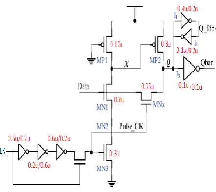
Figure 3. Modified pulse triggered D-FFRecalling the five circuits reviewed in Section II-A, they all encounter the same worst case timing occurring at 0 to 1 data transitions. Referring to Fig. 3 (proposed), Q-fdbk signal is not use modified circuit. The modified design adopts a signal feed-through technique to improve this delay. Similar to the conventional design, the modified design also employs a static latch structure and a conditional discharge scheme to avoid superfluous switching at an internal node. However, there are three major differences that lead to a unique TSPC latch structure and make the modified design distinct from the previous one. First, a weak pull-up pMOS transistor MP1 with gate connected to the ground is used in the first stage of the TSPC latch. This gives rise to a pseudo-nMOS logic style design, and the charge keeper circuit for the internal node X can be saved. In addition to the circuit simplicity, this approach also reduces the load capacitance of node X [4], [5]. Second, a pass transistor MNx controlled by the pulse clock is included so that input data can drive node Q of the latch directly. Along with the pull-up transistor MP2 at the second stage inverter of the TSPC latch, this extra passage facilitates auxiliary signal driving from the input source to node Q. The node level can thus be quickly pulled up to shorten the data transition delay. Third, the pull-down network of the second stage inverter is completely removed. Instead, the newly employed pass transistor MNx provides a discharging path. The role played by MNx is thus twofold, i.e., providing extra driving to node Q during 0 to 1 data transitions, and discharging node Q during “1” to “0” data transitions. Compared with the latch structure used in SCDFF design, the circuit savings of the modified design include a charge keeper (two inverters), a pull-down network, and a control inverter. The only extra component introduced is an nMOS pass transistor to support signal feed through. This scheme actually improves the “0” to “1” delay and thus reduces the disparity between the rise time and the fall time delays. In comparison with modified design to the other FF designs such as ep-DCO, CDFF, and SCDFF, Pulse Triggered D-FF(Fig.2) design shows the most balanced delay behaviors.
The modified flip flop designs are explained as follows. When a clock pulse arrives, if no data transition occurs, i.e., the input data and node Q are at the same level, on current
passes through the pass transistor MNx, which keeps the input stage of the FF from any driving effort. Therefore, no signal switching occurs in any internal nodes. On the other hand, if a “0” to “1” data transition occurs, node X is discharged to turn on transistor MP2, which then pulls node Q high. Referring to Figure. 1(b), this corresponds to the worst case timing of the FF operations as the discharging path conducts only for pulse duration. However, with the signal feed through scheme, a boost can be obtained from the input source via the pass transistor MNx and the delay can be greatly shortened. Although this seems to burden the input source with direct charging or discharging responsibility, which is a common pitfall of all pass transistor logic, the scenario is different in this case because MNx conducts only for a very short period. Referring to Fig. 1(c), when a “1” to “0” data transition occurs, transistor MNx is likewise turned on by the clock pulse and node Q is discharged by the input stage through this route. Unlike the case of “0” to “1” data transition, the input source bears the sole discharging responsibility. Since MNx is turned on for only a short time slot, the loading effect to the input source is not significant.
In particular, this discharging does not correspond to the critical path delay and calls for no transistor size tweaking to enhance the speed. In addition, since a keeper logic is placed at node Q, the discharging duty of the input source is lifted once the state of the keeper logic is inverted.
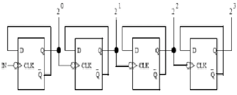
III- PROPOSED 4-BIT COUNTER
A counter, by function, is a sequential circuit consisting a set of flip-flops connected in a suitable manner to count the sequence of the input pulses presented to it in digital form. There are different kinds of counters.
Asynchronous Counter:
© 2015 IJEDR | Volume 3, Issue 3 | ISSN: 2321-9939
IJEDR1503012
International Journal of Engineering Development and Research (www.ijedr.org)4
Figure:4. 4-Bit Asynchronous CounterIV-SIMULATION RESULT
The comparison of result summarizes some important performance indexes of these Pulse Triggered D-FF designs as shown in Table 1. These include transistor count, Area, D to Q & D to Qbar propagation Delay, Power consumption and power delay product in 90-nm technology.
Table.1
© 2015 IJEDR | Volume 3, Issue 3 | ISSN: 2321-9939
IJEDR1503012
International Journal of Engineering Development and Research (www.ijedr.org)6
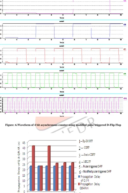
Figure: 6.Waveform of 4 bit asynchronous counter using modified pulse triggered D-Flip FlopIJEDR1503012
International Journal of Engineering Development and Research (www.ijedr.org)7
Figure 8.Power Consumption of flip flopsFigure 9.Power Consumption of flip flops
CONCLUSION
In this paper, we presented a 4 bit asynchronous counter implemented by employing a modified explicit type pulse triggered delay flip flop (D-FF) structure incorporating a mixed design style consisting of pass transistor and pseudo-nMOS logic. The pulse triggered flip flop (D-FF) was to provide a signal feed through from input source to the internal node of the latch, which would facilitate extra driving to shorten the transition time, avoids unnecessary Q_fdbk transistor and enhance both power and speed performance. Simulation results indicate that the modified design excels rival designs in performance indexes such as power, D-to-Q delay, and PDP.
REFERENCES
[1]A. G. M. Strollo, D. De Caro, E. Napoli, and N. Petra, “A novel high speed sense-amplifier-based flip-flop,” IEEE Trans. Very Large Scale Integer. (VLSI) Syst., vol. 13, no. 11, pp. 1266–1274, Nov. 2005.
[2] C. K. Teh, M. Hamada, T. Fujita, H. Hara, N. Ikumi, and Y. Oowaki, “Conditional data mapping flip-flops for low power and high-performance systems,” IEEE Trans. Very Large Scale Integer. (VLSI) Systems, vol. 14, pp. 1379– 1383, Dec. 2006.
[3] J. Tschanz, S. Narendra, Z. Chen, S. Borkar, M. Sachdev, and V. De, “Comparative delay and energy of single edge-triggered and dual edge triggered pulsed flip-flops for high-performance microprocessors, ” in Proc. ISPLED, 2001, pp. 207–212.
[4] H. Mahmoodi, V. Tirumalashetty, M. Cooke, and K. Roy, “Ultra low power clocking scheme using energy recovery and clock gating,” IEEE Trans. Very Large Scale Integr. (VLSI) Syst., vol. 17, no. 1, pp. 33–44, Jan. 2009.
[5] P. Zhao, J. McNeely, S. Venigalla, G. P. Kumar, M. Bayoumi, N. Wang, and L. Downey, “Clocked-pseudo-NMOS flip-flops for level conversion in dual supply systems,” IEEE Trans. Very Large Scale Integr. (VLSI) Syst., vol. 17, no. 9, pp. 1196–1202, Sep. 2009.
© 2015 IJEDR | Volume 3, Issue 3 | ISSN: 2321-9939
IJEDR1503012
International Journal of Engineering Development and Research (www.ijedr.org)8
[7] M.-W. Phyu, W.-L. Goh, and K.-S. Yeo, “A low-power static dual edge triggered flip-flop using an output-controlled discharge configuration,” in Proc. IEEE Int. Symp. Circuits Syst., May 2005, pp. 2429–2432.[8] Y.-T. Hwang, J.-F. Lin, and M.-H. Sheu, “Low power pulse triggered flip-flop design with conditional pulse enhancement scheme,” IEEE Trans. Very Large Scale Integr. (VLSI) Syst., vol. 20, no. 2, pp. 361–366, Feb. 2012.
[9] P. Zhao, T. Darwish, and M. Bayoumi, “High-performance and low power conditional discharge flip-flop,” IEEE Trans. Very Large Scale Integr. (VLSI) Syst., vol. 12, no. 5, pp. 477–484, May 2004.
[10] T. Indira, Ch. Jayaprakash“A Pulse Triggered flip flop using conditional pulse enhancement method for low performance application” International Conference on Recent Trends In Science And Technology-RTET-29th Sep 2013 – ISBN: 987-9381361-18-9.
[11] Y.-H. Shu, S. Tenqchen, M.-C. Sun, and W.-S. Feng, “XNOR-based double-edge-triggered flip-flop for two-phase pipelines,” IEEE Trans. Circuits Syst. II, Exp. Briefs, vol. 53, no. 2, pp. 138–142, Feb. 2006.
[12] V. G. Oklobdzija, “Clocking and clocked storage elements in a multigiga-hertz environment,” IBM J. Res. Devel., vol. 47, pp. 567–584, Sep.2003.
[13] S. H. Rasouli, A. Khademzadeh, A. Afzali-Kusha, and M. Nourani, “Low power single- and double-edge-triggered flip-flops for high speed applications,” IEE Proc. Circuits Devices Syst., vol. 152, no. 2, pp. 118–122, Apr. 2005.
[14] K. Chen, “A 77% energy saving 22-transistor single phase clocking D-flip-flop with adoptive-coupling configuration in 40 nm CMOS,” in Proc. IEEE Int. Solid-State Circuits Conf., Nov. 2011, pp. 338–339.
![Figure.1 Conventional Pulse Triggered D-FF designs. (a) ep-DCO [7]. (b) CDFF [16]. (c) Static-CDFF [17]](https://thumb-us.123doks.com/thumbv2/123dok_us/8370971.1384027/2.595.84.490.86.733/figure-conventional-pulse-triggered-designs-cdff-static-cdff.webp)