Electrical and optical characterization of Cd
x
Zn
1-
x
s thin
films deposited by chemical bath deposition in
alkaline conditions
Direct Research Journal of Chemistry and Material Science (DRCMS) Vol.2 (1), pp. 13-20, April 2014
ISSN 2354-4163
Available online at directresearchpublisher.org/drjcm ©2014 Direct Research Journals Publisher
Research Paper
*
Mosiori Cliff Orori, Njoroge Walter N. and Okumu John
Department of Physics, Kenyatta University,Nairobi, Kenya.
*Corresponding Author E-mail:cliffmosiori@gmail.com
Accepted 16 March 2014
In this work ternary CdZnS thin films were prepared by chemical bath deposition by doping CdS with different
concentrations of Zn ions. The chemical bath comprised of cadmium nitrate [Cd(NO3)2], as a source of Cd2+, zinc
nitrate [ZnNO3)2]as source of Zn2+, thiourea [(NH2)2CS] as a source of sulphide ions [S2-]in the presence of ammonia
[NH3] as a complexing agent. The competition mechanisms of Cd2+ and Zn+2 with the complexing agent [NH3] to
form complex ions usually plays a critical role in the formation of CdxZn1-xS thin films and therefore the influence of
Zn2+ on the formation mechanisms of the CdxZn1-xS was discussed. Optical and electrical properties of these
samples were analysed. Parameters like band gap (Eg), extinction coefficient (k), absorption coefficient (α),
dielectric constant (ε), refractive index, (n)and resistivity (ρ) were calculated using the data obtained from different
measurements. Optical band gap tunability of the deposited films for various Zn2+ concentrations was successfully
demonstrated by UV-VIS-NIR spectroscopy. Transmittance inCdxZn1-xSwas found to be above 80%, optical band
gap of 2.47-2.72 eV, refractive index of 2.58 – 2.39, and sheet resistivity of 1.09– 1.36 × 10² -cm for x = 1.0 – 0.6.
KEY WORDS: Chemical bath deposition, CdxZn1-xS, ZnS, CdS, electrical and optical properties, refractive index,
transmittance.
INTRODUCTION
The growth of ternary semiconductor thin films has been studied extensively in recent years. These films offer a higher performance prospects in semiconductor devices like photovoltaic cells and photo-conducting devices. Cadmium and zinc compounds are direct band gap
semiconductor materials suif for photovoltaic
applications. Cadmium zinc sulphide (CdxZn1-xS) has
been investigated as an important candidate for a wide band gap material. The replacement of CdS with a higher
energy gap ternary CdxZn1-xS has led to a decrease in
window absorption loss (Oztas and Bedir, (2005) and lattice mismatching with the Cu in GaSe and Cd Techalcopyrite semiconductors. While the band gap of
sulphide is based on a controlled release of the metal ions of Cd2+,Zn2+and sulphide ions (S2-) from thiourea in an aqueous alkaline bath. It is agreed that metal ions and sulphide ions are slowly released owing to the control of the complexing agent to form a thin film on the substrate. Only a few investigations have focused on the influence of growth parameters on the optical and electrical properties of the thin films prepared by CBD for photovoltaic cells. Song et al.,(2005) showed that the grain size of CdZnS films increase with increasing Zn content in the solution and thus influence the optical
properties of films. Gaewdang et al.(2004) investigated
the effects of a mixture ration x (x = [Zn2+]/[Cd2++Zn2+]) on the surface morphology, structure and transmission properties and found it to produce a decrease in the grain size with the increase in mixture ratio. The above investigations suggested that the concentration of Zn ions is an important factor influencing electrical and optical properties of thin films during the CBD process. In this
paper, CdxZn1-xS films were prepared by chemical doping
of CdS with different concentrations of Zn ions where the
concentration of Cd2+ was fixed while that of Zn2+ was
varied in the chemical bath. Optical and electrical properties of the samples prepared by CBD were analysed. This study shows how Zn influences these
optical and electrical properties of CdxZn1-xS thin films.
METHODOLOGY
The chemical bath constituents for the deposition of cadmium zinc sulphide included cadmium nitrate as
source of Cd2+, ammonium nitrate, zinc nitrate as source
of Zn2+and thiourea as source of S2. The bath was
composed of 0.038 M cadmium nitrate, 0.076 M ammonium nitrate, and 0.076 M thiuorea in de-ionised water. A 25 ml of the each solution was taken into a separate beaker and de-ionised water added to top up to
100 ml, then heated to about 82o C. Using a burette,
NH4OH (29.4%) was added drop-wise to the mixture to
maintain a pH of 9. Glass substrates were inserted at of
about 82o C for a deposition time of 25 min. Varying
concentrations of zinc nitrate [Zn(NO3)2] solutions were
added to the 100 ml beaker solution to vary zinc ions.
The value of x(x = Zn2+/[Cd2+ + Zn2+]) was varied from 1.0
- 0.6 where Zn varied from 0.0-0.4 according to the
equation CdxZn1-xS. A reaction mechanism for the
formation of CdS was suggested as below;
NH3 + H2O NH4 +
+ OH- (1) (a) Cadmium salts in the ammonium hydroxide solution form the complex compounds as:
Cd(NO4)2+4(NH3)Cd (NH3)4[NO3]2
Zn(NO4)2+4(NH3) (Zn(NH3)4)[NO3]2 (2)
Cd(NH3)4
2+
Cd2+ + 4NH3 (3)
Cd(OH)2 Cd + 2(OH)
Zn(OH)2 Zn2+ + 2(OH)- (4)
(b) From thiourea as a sulphide-ion source in an alkaline medium, the sulphide ions are to be released slowly as follows:
(NH2)2CS + 3OH
-
2NH3+ CO3
-2
+ S (5) SH- + OH- S-2 + H2O (6)
(c) Cadmium ions will then react with Sulphide and zinc
ions to form CdxZn1-xS from equations (3),(4), and (6):
x C d + 2+ (1-x)Zn2++ S-2 Cdx Zn1-xS (7)
Reactions in eq.1 to 7 are interrelated and indeed the ammonia concentration present affects the concentration
of cadmium ions Cd+2, the precipitation of cadmium
hydroxide [Cd(OH)2], the concentration of the
tetra-ammine-cadmium complex ion [Cd(NH3)2
+2
], and the
concentration of hydroxide ions [OH-]. Electrical
properties were studied using a four point probe connected to Kethley 2400 source meter interfaced with a
computer using Labviewprogram while optical
transmittance was measured using UV-VIS-NIR
spectrophotometer 3700.
RESULTS
Optical properties
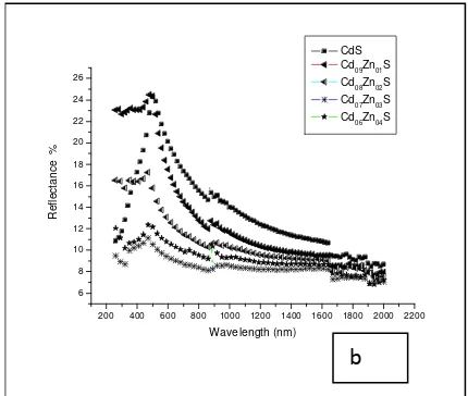
Films obtained by this method were smooth, uniform, adherent, bright yellow orange in colour where the yellowness decreased with increasing zinc content. CdS films had the highest reflectance and least transmittance
below 24% and 75% respectively. Cd06Zn04S films had
the least reflectance in the visible range (figure 1a,b,c and d). Doping the films using Zn reduced reflectance and absorbance but increased transmittance within the visible and infrared range. Refractive index (n) was
calculated using the equation proposed by Ravindra et
al., (2005) as
n = [(1+R1/2)/ (1-R1/2)] (8)
and one that relate optical refractive index (n) and energy
band gap (Eg) as;
n = 4.08 – 0.62Eg (9)
200 400 600 800 1000 1200 1400 1600 1800 2000 2200 0
20 40 60 80 100
Cd06Zn04S
T
ra
n
sm
it
ta
n
ce
%
W avelength (nm) CdS
Cd09Zn01S
Cd08Zn02S
Cd07Zn03S
Cd06Zn04S
a
Figure 1a Optical properties of CdxZn1-xS (x = 1.0 to 0.6).
200 400 600 800 1000 1200 1400 1600 1800 2000 2200
6 8 10 12 14 16 18 20 22 24 26
R
e
fl
e
ct
a
n
c
e
%
Wavelength (nm) CdS
Cd09Zn01S
Cd08Zn02S
Cd07Zn03S
Cd06Zn04S
b
Figure 1b. Optical properties of CdxZn1-xS (x = 1.0 to 0.6).
200 400 600 800 1000 1200 1400 1600 1800 2000 2200 0
20 40 60 80 100
A
b
s
o
rb
a
n
c
e
%
Wavelength [nm]
CdS
Cd09Zn01S
Cd
08Zn02S
Cd07Zn03S
Cd06Zn04S
c
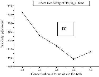
Table 1. Optical and electrical properties of CdxZn1-xS.
Film Conc. of Zn (n) Eg[eV] ρ[ -m]
Cd06Zn04S 0.4 2.39 2.72 136.19
Cd07Zn03S 0.3 2.41 2.69 122.91
Cd08Zn02S 0.2 2.46 2.60 116.98
Cd09Zn01S 0.1 2.51 2.52 109.37
CdS 0.0 2.53 2.47 113.56
State the meaning for n and if it has a unit indicate it.
0.0 0.1 0.2 0.3 0.4
2.38 2.40 2.42 2.44 2.46 2.48 2.50 2.52 2.54 2.56 2.58 2.60 2.62 2.64 2.66 2.68 2.70 2.72 2.74
R
e
fr
a
c
ti
v
e
i
n
d
e
x
[
n
]
a
n
d
B
a
n
d
g
a
p
[
Eg
]
Zn ion doping concentration [1-x]
---- Refractive index [n] ( Band gap [Eg])
d
Figure 1d. Optical properties of CdxZn1-xS (x = 1.0 to 0.6).
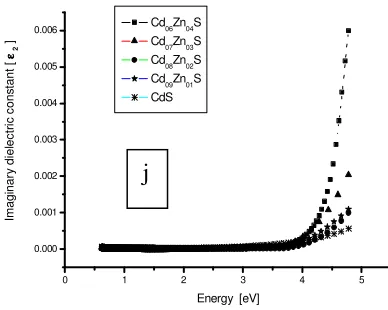
0 1 2 3 4 5
0.000 0.001 0.002 0.003 0.004 0.005
0.006 Cd06Zn04S
Cd 07Zn03S Cd
08Zn02S
Cd09Zn01S
CdS
Im
a
g
in
a
ry
d
ie
le
ct
ri
c
co
n
st
a
n
t
[ ε
εε ε 2
]
Energy [eV ]
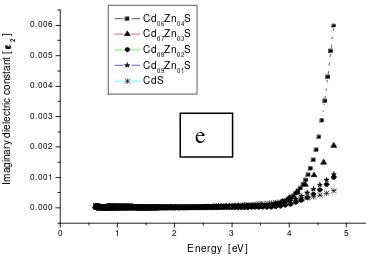
e
Figure 1e. Optical properties of CdxZn1-xS (x = 1.0 to 0.6).
optical conductivity (σ) in thin films where real and
imaginary parts of the dielectric constant are given by;
εc = εr + εi (10)
and they were estimated using the relations;
ε1 = n2 – k2 (11)
ε2 = 2nk (12)
The dielectric constant (ε) reduced as wave length
increased at a constant Zn concentration and it explains
0.6 0.7 0.8 0.9 1.0 2.50
2.55 2.60 2.65 2.70 2.75
B
a
n
d
g
a
p
E
g
[
e
V
]
Concentration, x [mol/lit]
CdxZn1-xS Band gap variation
f
Figure 1f. Optical properties of CdxZn1-xS (x = 1.0 to 0.6).
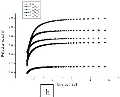
200 400 600 800 1000 1200 1400 1600 1800 2000 2200
1.0 1.2 1.4 1.6 1.8 2.0 2.2
R
e
fr
a
ct
iv
e
i
n
d
e
x
[
n
]
Wavelength [ nm ]
CdS
Cd09Zn01S
Cd08Zn02S
Cd07Zn03S
Cd06Zn04S
g
Figure 1g. Optical properties of CdxZn1-xS (x = 1.0 to 0.6).
0 1 2 3 4 5
1 .0 1 .2 1 .4 1 .6 1 .8 2 .0 2 .2
R
e
fr
a
c
ti
v
e
i
n
d
e
x
[
n
]
E n e rgy [ eV ] C dS
C d0 9Zn0 1S C d0 8Zn0 2S C d
0 7Zn0 3S C d0 6Zn0 4S
( b)
h
200 400 600 800 1000 1200 1400 1600 1800 2000 2200 1.0
1.5 2.0 2.5 3.0 3.5 4.0 4.5 5.0
R
e
a
l
d
ie
le
c
tr
ic
c
o
n
s
ta
n
t
[
ε]
W avelength [nm]
C dS
C d09Zn01S
C d08Zn02S
C d07Zn03S
C d 06Zn04S
i
Figure 1i. Optical properties of CdxZn1-xS (x = 1.0 to 0.6).
0 1 2 3 4 5
0.000 0.001 0.002 0.003 0.004 0.005
0.006 Cd06Zn04S
Cd07Zn03S
Cd08Zn02S
Cd09Zn01S
CdS
Im
a
g
in
a
ry
d
ie
le
c
tr
ic
c
o
n
st
a
n
t
[
ε ε ε ε2
]
Energy [eV]
j
Figure 1j. Optical properties of CdxZn1-xS (x = 1.0 to 0.6).
wavelengths (figure 1 f and g).The absorption coefficient
(α) was calculated using the equation;
α = 2.303A/d (13)
where α is the absorbance coefficient value at a particular
wavelength (λ) and d is the thickness of the
semiconductor film. Extinction coefficient on the other hand was calculated using the relation;
k = αλ/4π (14)
The both coefficients were very small over a wide range of wavelengths (figure 1 h, i and j) and as such very low photon energy absorption losses are experienced and thus form high quality window layer materials. Similar transmittance results have been reported (Kumar
and,(2009), Kasim et al. (2008), Saliha, (2009),Vidhya
and Velumeni, (2009) as 90%, 80%, 79% and 65% respectively in the wave length range of 300 – 1200 nm.
Band gap was determined by drawing a graph of (αhυ)2
versus the photon energy (hυ) plot.The intercept of the
curve with the photon energy (hυ) axis gave a direct band
gap by the Ugwu and Onah, (2007) relation:
α = (hv – Eg)1/2 / hv (15)
where h is Planck’s constant and hv is the photon energy.
They were obtained by extrapolating their linear portions
of the plots (αhv)2 versus hv to α= 0. They were
compared those obtained by modelling the Vergard’s
equation; Eg = [2.42 + 0.69x + 0.62x2] eV
200 400 600 800 1000 1200 1400 1600 1800 2000 2200 -3.5
-3.0 -2.5 -2.0 -1.5 -1.0 -0.5 0.0 0.5 1.0 1.5 2.0 2.5 3.0
lo
g
A
b
s
o
rp
ti
o
n
c
o
e
ff
ic
ie
n
t
[
lo
g
α
]
Wavelength [nm]
Cd06Zn04S
Cd07Zn03S
Cd08Zn02S
Cd09Zn01S
CdS
k
Figure 1k. Optical properties of CdxZn1-xS (x = 1.0 to 0.6).
200 400 600 800 1000 1200 1400 1600 1800 2000 2200
-9 -8 -7 -6 -5 -4 -3 -2 -1 0 1
lo
g
E
x
tin
ct
io
n
c
o
e
ff
ic
ie
n
t
[lo
g
k
]
Wavelength [nm]
Cd06Zn04S
Cd07Zn03S
Cd08Zn02S
Cd09Zn01S
CdS
l
Figure 1l.
Optical properties of Cd
xZn
1-xS (x = 1.0 to 0.6).
0.6 0.7 0.8 0.9 1.0
105 110 115 120 125 130 135 140
R
e
s
is
ti
v
it
y
,
ρ
[
o
h
m
-c
m
]
Concentration in terms of x in the bath
Sheet Resistivity of CdxZn1-xS films
m
where the value of x was modified from the ‘x’ to ‘(1-x)’ such that equation (12) appeared as eq. (13)
Eg=[2.42 +0.69(1-x) +0.62(1-x)2]eV (17)
The shift of absorption edge toward shorter wave lengths was due to increasing Zn giving rise to an increase in energy gap (Figure 1 k, l and m). The presence of the energy gap for pure CdS phase of about 2.43 eV seems
to be independent of the Zn ratio (x) and conversely,
CdxZn1-xS phase presents the variation of energy gap
from 2.50 to 2.72 eV when Zn ratio increases from 0.1 to 0.4. Table I shows that doped films had higher band gaps than pure CdS films. Cd06Zn04S had the greatest band gap of 2.72 eV while CdS had the least value of 2.47 eV
(figure 1e). This values agreed with Dzhafarov et al.
(2006)’s value of 2.64 eV for heavily doped CdxZn1-xS
films and Kasimet al. (2008) with an optimized value of
2.49 eV. Wider band gaps have been reported by Kumur and Sankaranayanan, (2009), Bacaksiz, (2006), (Vidhya and Velumini, 2009) and (Saliha, 2009) as 2.92 eV - 3.26 eV, 3.1 eV - 3.9 eV, 2.50 eV - 2.67 eV and 2.47 eV - 3.04 eV respectively.
CONCLUSION
CdxZn1-xS films were successfully prepared by solution
doping of CdS with different concentration of Zn ions. The
concentration of Cd2+ remained fixed which rendered it
possible to understand the effect of Zn ion concentration on the growth mechanism of the CdZnS film. The low
processing temperature used in CdxZn1-xS proposes that
CdxZn1-xS as window material could be used to fabricate
devices at low temperatures. Increase in transmittance was due increase in Zn ions in the bath resulting to band gaps of 2.47-2.72 eV. Refractive index decreased with Zn increase in the bath. Resistivity of the films increased with the increase in Zn concentration. The films were suitableas window layers for solar cells and opto-electronic devices.
ACKNOWLEDGEMENTS
I acknowledge the assistance offered by the Physics Department of Kenyatta University where this study was carried out. I also acknowledge the University of Nairobi department of Material Science [Chiromo Campus] for kindly providing the UV-VIS-NIR spectrophotometer 3700 for the spectral analysis of the thin films.
REFERENCES
Bacaksi E, Cevik U (2006). K-shell fluorescence yield of Cd and Zn in Cd1-xZnxS thin films on the structural, optical and electrical properties
of MW-CBD CdZnS thin films. American Journal of Nanotechnology,
123: 1-5
Dzhafarov T, Ougul F, Karabay I (2006). Formation of CdZnS thin films
by Zn diffusion. J. Phy. D: Appl. Phy. 39: 3221-3225.
Gaewdang N, Gaewdang T, Lipar W (2004). Some characterisation of
chemicalbath co-deposited CdS/ZnS thin films. Technical Digest
Inter. PVSEC, 14: 124 -126.
Kasim U, Narayanan H, Anthony O (2008).Optimization of process parameters of chemical bath deposition of Cd1-xZnxS thin
films.Leonardo Journal of Sciences, 12: 111-120.
Kumar T, Sankaranarayanan S (2009). Growth and characterisation of CdZnS thin films by short duration microwave assisted chemical bath
deposition technique. Chalcogenide Letters, 6: 555- 562.
Oztas M, Bedir M (2005).Some Properties of xZnxS and Cd1-xZnxS(In) Thin Films Prepared by Pyrolytic Spray Technique.Journal of Applied Sciences, 4: 534-537.
Ravindran N, Ganapathy P, Choi J (2006). Energy gap refractive index
relations in semiconductors – An overview. Elsevier Thin Solid Films:
Infrared Physics and Technology, 50: 21-79.
Saliha I, Muhsin Z, Yasemin C, Mujdat C (2009). Optical characterisation of the CdZn(S1-xSex)2 thin films deposited by spray
pyrolysis method. OpticaApplicata, XXXVI:1-9.
Song J, Thapa R , Maity R , Chattopadhyay K (2005) Optical and dielectric properties of PVA capped nanocrystallinePbS thin films
synthesized by chemical bath deposition.Thin Solid Films, 211: 14–21
Vidhya Y, Velumin A (2009). Electrical characterisation of chemically deposited thin films under magnetic field. Phys. Stat. Sol. 167: 143-151.
Ugwu I, Onah U (2007). Optical characteristics of chemical bath deposited CdS thin film characteristics within UV, Visible, and NIR
radiation. The Pacific Journal of Science and Technology, 8: