Western University Western University
Scholarship@Western
Scholarship@Western
Electronic Thesis and Dissertation Repository
12-13-2013 12:00 AM
Methods for Fabricating Printed Electronics with High
Methods for Fabricating Printed Electronics with High
Conductivity and High Resolution
Conductivity and High Resolution
Tengyuan Zhang
The University of Western Ontario
Supervisor Jun Yang
The University of Western Ontario
Graduate Program in Mechanical and Materials Engineering
A thesis submitted in partial fulfillment of the requirements for the degree in Master of Engineering Science
© Tengyuan Zhang 2013
Follow this and additional works at: https://ir.lib.uwo.ca/etd
Part of the Manufacturing Commons
Recommended Citation Recommended Citation
Zhang, Tengyuan, "Methods for Fabricating Printed Electronics with High Conductivity and High Resolution" (2013). Electronic Thesis and Dissertation Repository. 1842.
https://ir.lib.uwo.ca/etd/1842
This Dissertation/Thesis is brought to you for free and open access by Scholarship@Western. It has been accepted for inclusion in Electronic Thesis and Dissertation Repository by an authorized administrator of
METHODS FOR FABRICATING PRINTED ELECTRONICS WITH HIGH CONDUCTIVITY AND HIGH RESOLUTION
(Thesis format: Integrated Article)
by
Tengyuan Zhang
Graduate Program in Mechanical & Materials Engineering
A thesis submitted in partial fulfillment of the requirements for the degree of
Master of Engineering Science
The School of Graduate and Postdoctoral Studies The University of Western Ontario
London, Ontario, Canada
Abstract
Flexible and printable electronics are attractive techniques which are believed to be
widespread and occupy huge market. However, low conductivity, nozzle clog because of
the accumulation of nano-particles and relative high cost (expensive silver/copper
nanoparticle inks) limit its appeal. In this thesis, two new effective and convenient
methods of fabricating copper patterns with high conductivity and strong adhesion on
flexible photopaper and polymer substrates (PET) are demonstrated, solving all those
problems. Functional photopaper and PET substrate was prepared with inkjet printing of
a palladium salt solution and hyperthermal hydrogen induced cross-linking (HHIC)
polyelectrolytes onto its surface respectively, followed by electroless deposition of
copper, creating high quality flexible copper patterns on different substrates. The
developed technique was successfully applied for fabricating functional flexible circuits
such as radio frequency identification devices (RFID) antenna, micro-inductive coil and
complex circuit board.
Keywords
Printed electronics, electroless deposition, inkjet printing, screen printing, flexible
circuits, low-cost fabrication, high conductivity copper circuits, hyperthermal hydrogen
induced cross-linking (HHIC)
Co-Authorship Statement
This master thesis has been prepared according to the regulations for an integrated article
format thesis stipulated by the Faculty of Graduate and Postdoctoral Studies at the
University of Western Ontario and has been co-authored as follows:
Chapter 2: Fabrication of flexible high resolution copper patterns on
photopaper
All the theoretical analyses and experiments were conducted by T. Zhang. A draft of
Chapter 2 was prepared by T. Zhang. Dr. Yang and Dr. Wang helped revising the
manuscript. Dr. Guo and T. Li got involved in many of our discussions and provided
many valuable ideas about this project. A paper entitled Fabrication of flexible
copper-based electronics with high-resolution and high-conductivity on paper via inkjet
printing (T. Zhang, X. Wang, and et al.) has been published in the Journal of Materials
Chemistry, 2013. The patent regarding this technique has been filed.
Chapter 3: Fabrication of flexible high conductivity copper patterns on
polymer substrate
All the theoretical analyses were conducted by T. Zhang. All the experiments were
conducted by T. Zhang collaborating with Dr. Wang. A draft of Chapter 3 was prepared
by T. Zhang. Dr. Wang and Dr. Yang helped revising the manuscript. A paper entitled
Grafting polyelectrolytes to hydrocarbon surfaces by hyperthermal hydrogen in
induced cross-linking for making metallized polymer films (X. Wang, T. Zhang, et al.)
has been published in Chemical Communication, 2013.
Acknowledgments
First I would like to express my sincere gratitude to my advisor Prof. Jun Yang for his
help and continuous support of my master study and research. He not only helped me a
lot on courses and experiments but also taught me how to be a qualified researcher, a
responsible man for both his work and life. His enthusiasm, patience, diligent, immense
knowledge and his ways of doing things are always my guidance in all the time of my
study here in Western University.
Besides my advisor, I would like to thank Prof. Xiaolong Wang and Dr. Qiuquan Guo for
helping me on my writing work and research. They answered me a lot of questions and
trained me for using lots of equipment though they are very busy. My sincere thanks also
goes to Dr. Xiaobin Cai, Dr. Peipei Jia, Mr.Zhaoliang Yang, Mr.Luyang Zhang and Mr.
Usman Jamil Rajput for the brain storm discussions, for many sleepless nights we were
working together before deadlines, also I thank all my friends, for all the fun we have had
in the past year.
Last but not the least, I would like to thank my family: my mom and dad for always
supporting me in all ways; my girlfriend, Mengmeng Zhang who is always standing by
my side sharing all my happiness and sorrow. Without any of you, I would never go this
far.
Table of Contents
Abstract ... ii
Co-Authorship Statement... iii
Acknowledgments... iv
Table of Contents ... v
List of Tables ... viii
List of Figures ... ix
Preface... xiii
Chapter 1 ... 1
1 Introduction ... 1
1.1 Research motivation... 1
1.2 Background and literature review ... 3
1.3 Research objectives ... 6
1.3.1 Objective 1: Developing a new method to fabricate printed electronics solving several critical issues ... 7
1.3.2 Objective 2: Fabricate flexible copper patterns on polymer based substrate (PET)... 8
1.4 References ... 10
Chapter 2 ... 14
2 Fabrication of flexible high resolution copper patterns on photopaper ... 14
2.1 Introduction ... 14
2.2 Theory ... 17
2.2.1 Inkjet printing... 17
2.2.2 Electroless deposition ... 21
2.3 Materials and experiments set-up ... 21
2.3.1 Materials ... 21
2.3.2 Preparation of the palladium salt ink ... 22
2.3.3 Inkjet printing and parameters optimization ... 23
2.3.4 ELD of copper and thermal sintering... 25
2.3.5 Characterization ... 26
2.4 Results and discussion ... 26
2.4.1 Ink viscosity and stability ... 26
2.4.2 Inkjet printing of salt solution ... 31
2.4.3 ELD and conductivity ... 35
2.5 Conclusion ... 50
2.6 References ... 52
Chapter 3 ... 56
3 Fabrication of high conductivity flexible copper patterns on PET ... 56
3.1 Introduction ... 56
3.2 Theory ... 59
3.2.1 Hyperthermal hydrogen induced cross-linking (HHIC) ... 59
3.3 Experiments and discussion ... 60
3.3.1 Procedure ... 60
3.3.2 Materials ... 62
3.3.3 Fabrication of copper patterns on PET ... 62
3.3.4 Characterization ... 63
3.3.5 Results and discussion ... 65
3.4 Conclusion ... 76
3.5 References ... 77
Chapter 4 ... 80
4 Summary and future work ... 80
4.1 Summary ... 80
4.2 Thesis contributions ... 82
4.3 Future work ... 82
Curriculum Vitae ... 84
List of Tables
Table 1: ELD of copper results of patterns printed with different concentration (Scale bar: 1 cm) ... 36
List of Figures
Figure 1: Schematic illustration of paper-based metal patterns with high resolution and
conductivity via printing catalyst and subsequent ELD process. ... 17
Figure 2: Principle of continuous inkjet printer. (Copy from [26]) ... 19
Figure 3: Principle of drop-on-demand inkjet printer. (Copy from [10]) ... 20
Figure 4: Dimatix DMP-2800 DOD inkjet printer used for this project... 20
Figure 5: VWR mixer ... 22
Figure 6: Gilmont GV-2100... 23
Figure 7: Fisher 1500 DEG Tube Furnace ... 25
Figure 8: Viscosity of inks with different Pd salt concentration ... 29
Figure 9: UV/visible-spectra (fitted) results of freshly prepared palladium (II) salt ink (triangle facing down) and inks after storage at room temperature for 8 hours (triangle facing up), 3 days (round circle), 180 days (square) and 180 days stored under 4 °C (diamond) ... 30
Figure 10: Droplets pictures under different jetting conditions (a) Misdirected jetting caused by accumulated leaked ink around the nozzle. (b) Satellite droplets caused by relative high jetting voltage. (c) Droplets after applying the optimum parameters (meniscus vacuum: 3.5 H2O, jetting voltage peak ~24.30 V, single jetting duration: 32.192 µs (phase 1: 9.792 µs, phase 2: 6.160 µs, phase 3: 8.496 µs, phase 4: 5.184 µs), maximum jetting frequency: 20 kHz). ... 34
Figure 11: Modified waveform for the ammonium tetrachloropalladate (II) ink ... 35
Figure 12: SEM image of the cross section of the ELD copper layer on photopaper ... 38
Figure 13: High resolution complex flexible circuit board on photopaper ... 40
Figure 14: Integrated test pattern of the new printed electronics fabrication method ... 40
Figure 15: Microscope image of a part of the high resolution printed circuit board ... 41
Figure 16: Microscope image of a part of micro inductive coil fabricated by the proposed method... 41
Figure 17: Conductivity measurement results of patterns under different conditions by four-probe method (bending curvature 1 cm-1) ... 42
Figure 18: SEM image of un-sintered copper pattern on photopaper substrate ... 43
Figure 19: SEM image of sintered copper pattern on photopaper substrate ... 44
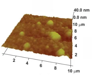
Figure 20: AFM 3D image of the copper surface (before sintering) ... 46
Figure 21: AFM 3D image of the copper surface (after sintering) ... 46
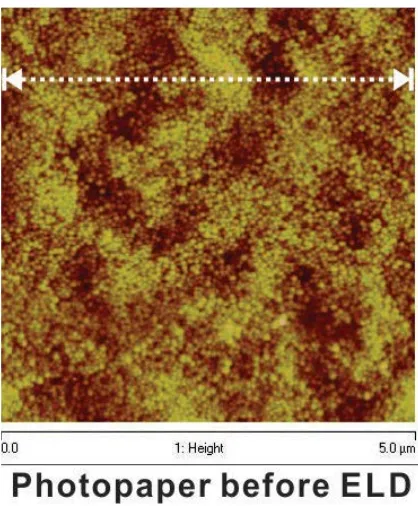
Figure 22: AFM height information images of copper (before sintering), photopaper after ELD bath and photopaper before ELD ... 49
Figure 23: AFM Section profile of selected parts showing in Fig. 22 with white dash lines, corresponding to the copper, photopaper after ELD and photopaper before ELD one by one. ... 49
Figure 24: XRD patterns of photopaper, copper on photopaper after sintering and copper on photopaper before sintering ... 50
Figure 25: Schematic of polyelectrolyte molecules (PMETAC in this case) grafting to hydrocarbon surface by HHIC followed by ELD to create high quality copper patterns on PET substrate ... 58
Figure 26: Schematic illustration of the mechanism of HHIC ... 60
Figure 27: Schematic illustration of the proposed procedure in micro level ... 61
Figure 28: Kratos AXIS Ultra and AXIS Nova (Copyright: Surface Science Western,
Western University) ... 64
Figure 29: Nanoscope V Atomic force microscopy (AFM) ... 64
Figure 30: Conductivity measurement setup: four-probe station (a) connected to M 2400 Keithley Multimeter (b) ... 65
Figure 31: XPS results of Cu-PET, Pd-loaded-PET, PMETAC-PET, and raw PET... 66
Figure 32: XPS high resolution spectra of N 1s ... 66
Figure 33: XPS high resolution spectra of Pd 3d ... 67
Figure 34: AFM height information of raw PET ... 68
Figure 35: AFM images of PMETAC-PET ... 69
Figure 36: AFM images of Cu-PET... 69
Figure 37: AFM images of Cu-PET (a), and SEM images of Cu-PET(b) in different scale ... 70
Figure 38: Photos of Scotch tape test before (a) and after (b) three times peeling-off ... 70
Figure 39: AFM image of PMETAC-PET obtained on 9.9 nm thick coating ... 72
Figure 40: AFM image of PMETAC-PET obtained by HHIC exposure on 42.7 nm-thick PMETAC coating. The Z-scale is 100 nm ... 72
Figure 41: Thickness of Cu films obtained at 10 min of ELD on PMETAC-PET surfaces based on PMETAC coating with initiate thickness of 9.9 nm, 26.8 nm, and 42.7 nm before HHIC exposure ... 73
Figure 42: Thickness of Cu films as function of ELD time ... 74
Figure 43: Photos of patterned Cu lines on PET (a) and the integrated circuit operated under bending (b) ... 75
Figure 44: Patterned Cu lines on PDMS film ... 76
Preface
Studying in the University of Western Ontario is truly an amazing experience for me. 14
months ago I joined Dr. Yang’s group and became a member of the BioNano Technology
Lab, 2 months later I started this project and began my journey in the area of the printed
electronics. At that time, I never thought that I would publish my own paper and let other
people who are also fighting in this area hear my voice. But it finally came true, after all
those days and nights spent in the lab, fighting shoulder to shoulder with my fellow
scientists and colleagues, the hope for good results, the disappointment of each failed
attempt and the joy of weekends.
I always consider myself as a lucky dog, and this time will be no exception. I feel lucky
to have the opportunity to follow Dr. Yang, who is an amazing supervisor, for my master
degree and contribute as a member in his group. We always say that a good teacher
should not only propagate the doctrine, impart professional knowledge, but also should
resolve doubts. Well, Dr. Yang did all of them, he is not only our research leader but also
our mentor in life. He taught me how to do the research, and what’s more, he also helped
me to find out why I should do that, which I think is more important. In Dr. Yang’s
group, you are not alone, because we work together, solve each problem together and
share the joy of success together.
Time is always flying and efforts will make the past days become memorable. I treasure
all the people who ever helped me and are supporting me.
This thesis is dedicated to all of you.
Chapter 1
1
Introduction
1.1 Research motivation
Flexible electronics/devices, which can maintain functionality when subject to a large
deformation or stress, represent an important direction of future electronics
manufacturing and mechanical engineering. Wearable, rollable and foldable displays,
sensors, solar cells, batteries and other flexible electronics/devices will bring us
completely different user experience and even change our daily life. For example,
wearable or implantable biomedical devices can be the next generation tools for heath
monitoring, disease diagnostics and treatment. Several strategies have been developed to
make flexible and stretchable electronics/devices. For example, one approach is to use
organic conductive or semiconducting materials, or inorganic thin films or
one-dimensional nanomaterial that can flex. Another approach is to integrate conventional
high-performance silicon based electronic components with optimized structural
configurations such as wavy shapes that can absorb the induced deformation. A lot of
effort has also been focused on the fabrication of flexible electrical circuits that can be
stretched, twisted or compressed. When functional components such as light emitting
diodes (LEDs) connected and powered by such circuit are bended, twisted and
compressed the circuits deform to offer the flexibility allowance of the whole device
while the central functioning components are in fact subject to very small stress.
However many of these studies are still in infancy and mostly rely on sophisticated and
expensive nano/micro fabrication processes and facilities, and involve high processing
temperatures and toxic wastes. It is therefore highly desirable, yet extremely challenging,
to develop low-cost and scalable facile methods that can operate at low processing
temperatures and use inexpensive materials to make integratable, flexible or even
stretchable electronics and devices.
Recently, several printing techniques, including inkjet printing, nanoimprinting and
screen printing, have emerged as a very promising technical trend to produce flexible and
stretchable electronics/devices. Especially for the material or inkjet printing as an
additive manufacturing method, it has proved to be very versatile and cost-effective for
making flexible and stretchable electronics via a direct writing manner with merits of
high efficiency, low material consumption and programmable control. However
challenges remain in low conductivity of printed circuits, instable printing due to nozzle
clog and misdirection jetting, weak adhesion between the printed materials and the
substrates, low resolution, limited choices of substrate materials, and relatively high cost
due to the use of Ag or Au nanoparticle based conductive inks. Particularly the low
conductivity and instable printing problems directly affect the quality control during the
manufacturing, and performance and lifetime of the devices, causing fatal functional
failure of the printed circuits or devices. If the printing resolution can be improved, cost
and material consumption will be reduced, throughput will be further increased, and
many more applications will become available.
There is increasing demand for high quality and low cost electronic components such
as RFID tags, thin film transistor, super capacitor, flexible sensor and devices, which
require innovative fabrication techniques that are faster but cheaper compared to
traditional production methods. [1-3] It is also predicted that the market of flexible
organic and printed electronics will exceed $300 billion by 2028. [4] So a new generation
technique of fabricating flexible printed electronics which can overcome all those
problems mentioned above in badly need.
This thesis presents a new developed ultra-low-cost method of inkjet printing combined
with electroless deposition (ELD) process to prepare high-resolution high-conductivity
copper patterns on flexible photopaper substrate, overcoming almost all the problems that
the industry of printed electronics is facing today
1.2 Background and literature review
It has been demonstrated that flexible or stretchable printed electronics/devices are
opening up many exciting opportunities, [5, 6] such as wearable electronics, [7] skin
sensors [8, 9] and biological actuators etc. [10] The key to realize flexibility or
stretchability of electronics/devices is the integration of excellent mechanical robustness
with electrical/electronic performance. Rigid materials like silicon may exhibit good
electrical/electronic performance and stability, but have poor mechanical ductility. On the
other hand, soft materials show excellent mechanical deformability while having
unsatisfactory electrical and electronic properties. And it is almost impossible for the
conventional manufacturing process to fabricate electronics on flexible or stretchable
substrate such as PET, PI, photopaper and PDMS.
Several strategies have been suggested to address the challenges. For example, one can
configure conductive thin films or ribbons into in-plane waves or out-of-plane buckles
and then bond onto polymeric substrates to realize flexible electronics/devices. Various
flexible electronic devices have been developed by using the buckled, serpentine
structures of silicon or metals as interconnects or electrodes. [11-13] Although flexibility
and even stretchability up to 70% strain have been achieved, the drawback of this
strategy is the complicated micro/nanofabrication processes. Another strategy, filling
polymeric or rubbery matrix with conductive materials, is a less-costly method to make
flexible and stretchable conductive composites. The conductive materials can be metals,
[14, 15] conductive polymers [16] and carbon materials. [17-21] Although this strategy
can easily yield flexible conductors and electronics, the disadvantages are also obvious
including low conductivity and the change of conductivity under stress. The normal trend
is that the conductivity decreases under bending. However non-monotonic piezoresistive
behavior, which is counter-intuitive, has also been observed in many conductive polymer
nanocomposites. [22-24] Under stretching or other types of mechanical deformation, the
conductive fillers behave differently from the polymer phase in terms of mechanical
responses. This induces re-distribution and/or re-orientation of nanofiller, deboning or
rebonding at nanofiller-polymer interfaces. Consequently, electron transport mechanisms,
including conducting path mechanism and electron hopping or tunneling effect, are
significantly changed, leading to the change of the conductive properties of the
nanocomposites. This mechanism is complex and has not yet been fully understood.
Therefore the quality control becomes difficult if the electronics/devices are made based
on this strategy.
Conventional electronic fabrication systems are mostly based on photolithography, a
complex and time-consuming process that involves large volumes of hazardous
waste and expensive facilities, what' more, it cannot be used for fabricating electronics
on various substrate especially those flexible, easy corrosion but environmental friendly
substrates. In this regard, the strategy of coating conductive materials onto polymers or
elastomers, has emerged as a very promising method, which enables fabrication of
flexible or stretchable electronics in a low-cost and scalable manner. [25-28] Various
technologies have been emerged as promising technical trends to produce flexible
electronics and devices including spray coating, [25] physical deposition, [26, 27]
chemical deposition, inkjet printing, [29] non-vacuum deposition, [30] screen printing
etc. [31] Among these, inkjet printing technology has gained more and more attention in
recent years for its appeal of low-cost, non-contact, scale-up capability, low material and
energy consumption, programmable control and maskless additive manufacturing.
Various flexible and stretchable electronics have been inkjet printed in a laboratory
setting using carbon nanomaterial, [32, 33] conductive polymers, [34] metal
nanoparticles [35] and liquid metals. [36] Due to its versatility and cost-effectiveness,
inkjet printing has become one of the most promising methods for fabrication of flexible
and stretchable electronics.
However delamination or peeling-off is always a concern because the conductive
materials are typically deposited on the top of substrates only. The possibility of failure
under repeated mechanical loading limits its applications in areas where reliability and
stability are important. In addition, unsatisfactory conductivity of printed materials that is
far below that of the bulk material is another major problem. Applied to printed
electronics based on inkjet printing, most of the research efforts are focused on
direct printing of metal nanoparticles or conductive polymer, followed by sintering to
make them conductive. Copper or silver nanoparticle based inks were commonly
printed on a treated PET/PI substrate, with a nozzle size of larger than 15 µm, and
dimension of the final resulted metal pattern is normally around 10-20 µm, five times
better than the current resolution of screen printing. However, clogging is always a
common critical issue for micron size nozzles due to the accumulation of nanoparticles at
the nozzle opening caused by interactive force. Other critical issues reside in the
oxidization and sedimentation stability of the corresponding inks, generally requiring
large amounts of stabling and decoration agent and is thus in a very low concentration of
metal particles which consequently leads to a high resistance of the printed patterns. [37,
38] Extensive research and development are required to overcome these technical hurdles
to advance the material printing technology to the state of the art manufacturing process.
For example, how to improve conductivity and resolution of printed circuits, improve
adhesion between the printed materials and the substrates, further reduce the cost, and
enrich choices of substrate materials, are all key issues that remain to be solved. Thus it’s
strategically important to develop robust, high-resolution, high-performance and low-cost
material printing technologies, which enable a broader variety of substrate materials,
good electrical and electronic performance close to conventional electronics, and the use
of inexpensive metals like copper.
1.3 Research objectives
The main purpose of our research is to develop new techniques that present competitive
advantages over nowadays printed electronics fabrication technologies in terms of
conductivity, resolution, material-substrate adhesion and variety of choices of substrates.
We are aiming at pushing forward the board of the printed electronics industry, solving
the problems of printed electronics fabrication that we are facing today. We believe that
the printed electronics will completely replace conventional PCB fabrication technology
if some of the technical issues were solved. So we started this work, trying to make our
own contributions to the development of human technology.
1.3.1 Objective 1: Developing a new method to fabricate printed
electronics solving several critical issues
The most common printed electronics fabrication technology is to inkjet print
Ag-nanoparticle or Cu-Ag-nanoparticle based inks, where the nozzle size is typically larger than
10 µm, and the line and space dimension is normally around 10 µm and 20 µm,
respectively. The nozzle size is one of key factors that determine the resolution of inkjet
printing. Ideally the smaller the nozzle size, the higher the printing resolution. However
clogging is always a common issue for micron size nozzles due to accumulation of
nanoparticles at the nozzle opening. Ag inks are popular mainly because they are stable
and sintering of Ag nanoparticles can take place at low temperature around 150 ºC.
However Ag is still relatively expensive compared to Cu. Our goal is to print inexpensive
metals like Cu with good conductivity and with high printing resolution. Here we propose
to print catalyst (noble-metal-containing salt) solution instead of conductive inks which
are a complex mixture of nanoparticles, stabling agent, solvent and other additives.
Printing pure catalyst noble-metal-containing salt solution eliminates the issue of nozzle
blocking and allows us to use smaller and even nanometer scale printer head nozzle to
greatly improve the printing resolution. Therefore the new approach offers a promise to
achieve a breakthrough printing resolution. After printing catalyst, the substrate is
immersed in Cu salt solution and electroless deposition will occur to deposit Cu
nanoparticles on the substrate according to the printed patterns.
Effects of concentration of the palladium salt on the viscosity and surface tension of the
ink, effects of ELD time on the surface morphology and conductivity will be
investigated. Jetting program of material printers like the voltage control waveform,
jetting frequency, meniscus vacuum level, printing height, temperature of the printhead
and substrate etc. will be optimized according to achieve a reliable, high resolution
printing. Scanning electron microscope (SEM), XRD (X-ray Diffraction) and Atomic
force microscope (AFM) will be used to conduct material/chemical/surface analyses for
each step of this new printing process.
1.3.2 Objective 2: Fabricate flexible copper patterns on polymer
based substrate (PET)
We achieved objective 1 through efforts, functional copper patterns with high resolution
and high conductivity were successfully fabricated on flexible photopaper substrate. But
the photopaper substrate still has many limitations, for example it is easy to be torn, burn
and corroded. What’s more, we believe the relative rough surface of the photopaper limit
the conductivity of deposited copper. So we decided to push the board of printed
electronics forward and set our goal to make high conductivity copper patterns on PET
substrate, a stable, smooth and transparent polymer based substrate.
While for the photopaper, it is relative easy to plant functional groups on its surface using
a surface treatment method and this kind of surface treatment technique is mature in the
industry. But for some other polymer based substrate such as PET/PI, the conventional
wet chemical polyelectrolyte treatment process doesn’t work well, since such substrate is
chemically inert and you need to put lots of effort to make it active. What’s more,
conventional wet chemical surface treatment techniques create lots of chemical waste and
most of them is hazardous and harmful to human body. So we tried to propose another
surface treatment process to form metallic circuits on hydrocarbon polymers using a
unique hyperthermal hydrogen induced cross-linking (HHIC) technology to graft
polyelectrolyte on polymers which is an environmental friendly, chemical-free method to
achieve a strong adhesion between the deposited materials and the substrate. [39-42]
After HHIC, the printed solution will bond together with the substrate, creating high
conductivity copper patterns which have a very strong adhesion with the PET substrate
after ELD process.
The proof-of-concept work was demonstrated in Chapter 3. The feasibility and merit of
this printing process is that the grafted polyelectrolyte will act as an effective linker layer
connecting the polymer substrate with the metal layer, resulting in a very strong adhesion
between the deposited copper and the PET or PDMS substrate. The methodology will be
also applied to other commercially available polymeric materials such as PC
(polycarbonate), PE (Polyethylene), PVC (Polyvinyl chloride) and PI (Polyimide).
1.4 References
[1] J. Perelaer, P. J. Smith, D. Mager, D. Soltman, S. K. Volkman, V. Subramanian, et al., "Printed electronics: the challenges involved in printing devices,
interconnects, and contacts based on inorganic materials," Journal of Materials Chemistry, vol. 20, pp. 8446-8453, 2010.
[2] X. Wang, T. Li, J. Adams, and J. Yang, "Transparent, stretchable, carbon-nanotube-inlaid conductors enabled by standard replication technology for capacitive pressure, strain and touch sensors," Journal of Materials Chemistry A,
vol. 1, pp. 3580-3586, 2013.
[3] X. Li, G. Wang, X. Wang, X. Li, and J. Ji, "Flexible supercapacitor based on MnO2 nanoparticles via electrospinning," Journal of Materials Chemistry A, vol. 1, pp. 10103-10106, 2013.
[4] D. Lupo, W. Clemens, S. Breitung, and K. Hecker, "OE-A Roadmap for Organic and Printed Electronics," in Applications of Organic and Printed Electronics, E. Cantatore, Ed., ed: Springer US, 2013, pp. 1-26.
[5] T. Sekitani and T. Someya, "Stretchable, Large-area Organic Electronics,"
Advanced Materials, vol. 22, pp. 2228-2246, May 25 2010.
[6] J. A. Rogers, T. Someya, and Y. G. Huang, "Materials and Mechanics for Stretchable Electronics," Science, vol. 327, pp. 1603-1607, Mar 26 2010.
[7] H. L. Filiatrault, G. C. Porteous, R. S. Carmichael, G. J. E. Davidson, and T. B. Carmichael, "Stretchable Light-Emitting Electrochemical Cells Using an Elastomeric Emissive Material," Advanced Materials, vol. 24, pp. 2673-2678, May 22 2012.
[8] A. E. Aliev, J. Y. Oh, M. E. Kozlov, A. A. Kuznetsov, S. L. Fang, A. F. Fonseca, et al., "Giant-Stroke, Superelastic Carbon Nanotube Aerogel Muscles," Science,
vol. 323, pp. 1575-1578, Mar 20 2009.
[9] D. H. Kim, N. S. Lu, R. Ma, Y. S. Kim, R. H. Kim, S. D. Wang, et al., "Epidermal Electronics," Science, vol. 333, pp. 838-843, Aug 12 2011.
[10] F. Ding, H. Ji, Y. Chen, A. Herklotz, K. Dörr, Y. Mei, et al., "Stretchable
graphene: a close look at fundamental parameters through biaxial straining," Nano letters, vol. 10, pp. 3453-3458, 2010.
[11] X. Wang, H. Hu, Y. Shen, X. Zhou, and Z. Zheng, "Stretchable conductors with ultrahigh tensile strain and stable metallic conductance enabled by prestrained polyelectrolyte nanoplatforms," Advanced Materials, vol. 23, pp. 3090-3094, 2011.
[12] Y. Xia, B. Gates, Y. Yin, and Y. Lu, "Monodispersed colloidal spheres: old materials with new applications," Advanced Materials, vol. 12, pp. 693-713, 2000.
[13] K. Nomura, H. Ohta, A. Takagi, T. Kamiya, M. Hirano, and H. Hosono, "Room-temperature fabrication of transparent flexible thin-film transistors using
amorphous oxide semiconductors," Nature, vol. 432, pp. 488-492, 2004.
[14] D. C. Hyun, M. Park, C. Park, B. Kim, Y. Xia, J. H. Hur, et al., "Ordered zigzag stripes of polymer gel/metal nanoparticle composites for highly stretchable conductive electrodes," Advanced Materials, vol. 23, pp. 2946-2950, 2011.
[15] D. H. Kim and J. A. Rogers, "Stretchable electronics: Materials strategies and devices," Advanced Materials, vol. 20, pp. 4887-4892, 2008.
[16] Z. Yu, Q. Zhang, L. Li, Q. Chen, X. Niu, J. Liu, et al., "Highly Flexible Silver Nanowire Electrodes for Shape‐Memory Polymer Light‐Emitting Diodes,"
Advanced Materials, vol. 23, pp. 664-668, 2011.
[17] Z. Zhang, C. Shao, P. Zou, P. Zhang, M. Zhang, J. Mu, et al., "In situ assembly of well-dispersed gold nanoparticles on electrospun silica nanotubes for catalytic reduction of 4-nitrophenol," Chem. Commun., vol. 47, pp. 3906-3908, 2011.
[18] Z. Liu, S. Tabakman, K. Welsher, and H. Dai, "Carbon nanotubes in biology and medicine: in vitro and in vivo detection, imaging and drug delivery," Nano research, vol. 2, pp. 85-120, 2009.
[19] K. S. Kim, Y. Zhao, H. Jang, S. Y. Lee, J. M. Kim, K. S. Kim, et al., "Large-scale pattern growth of graphene films for stretchable transparent electrodes," Nature,
vol. 457, pp. 706-710, 2009.
[20] T. Sekitani, Y. Noguchi, K. Hata, T. Fukushima, T. Aida, and T. Someya, "A rubberlike stretchable active matrix using elastic conductors," Science, vol. 321, pp. 1468-1472, 2008.
[21] Y. Zhang, C. J. Sheehan, J. Zhai, G. Zou, H. Luo, J. Xiong, et al., "Polymer‐ Embedded Carbon Nanotube Ribbons for Stretchable Conductors," Advanced Materials, vol. 22, pp. 3027-3031, 2010.
[22] S. Eichhorn, A. Dufresne, M. Aranguren, N. Marcovich, J. Capadona, S. Rowan, et al., "Review: current international research into cellulose nanofibres and nanocomposites," Journal of Materials Science, vol. 45, pp. 1-33, 2010.
[23] D. Bloor, K. Donnelly, P. Hands, P. Laughlin, and D. Lussey, "A metal–polymer composite with unusual properties," Journal of Physics D: Applied Physics, vol. 38, p. 2851, 2005.
[24] J. Busfield, A. Thomas, and K. Yamaguchi, "Electrical and mechanical behavior of filled elastomers 2: The effect of swelling and temperature," Journal of Polymer Science Part B: Polymer Physics, vol. 42, pp. 2161-2167, 2004.
[25] D. J. Lipomi, M. Vosgueritchian, B. C. Tee, S. L. Hellstrom, J. A. Lee, C. H. Fox, et al., "Skin-like pressure and strain sensors based on transparent elastic films of carbon nanotubes," Nature nanotechnology, vol. 6, pp. 788-792, 2011.
[26] G. Catalan and J. F. Scott, "Physics and applications of bismuth ferrite,"
Advanced Materials, vol. 21, pp. 2463-2485, 2009.
[27] D. Yoon, Y.-W. Son, and H. Cheong, "Strain-dependent splitting of the double-resonance Raman scattering band in graphene," Physical Review Letters, vol. 106, p. 155502, 2011.
[28] D. S. Germack, C. K. Chan, B. H. Hamadani, L. J. Richter, D. A. Fischer, D. J. Gundlach, et al., "Substrate-dependent interface composition and charge transport in films for organic photovoltaics," Applied Physics Letters, vol. 94, p. 233303, 2009.
[29] A. Teichler, J. Perelaer, and U. S. Schubert, "Inkjet printing of organic electronics - comparison of deposition techniques and state-of-the-art developments," Journal of Materials Chemistry C, vol. 1, pp. 1910-1925, 2013.
[30] A. R. Uhl, C. Fella, A. Chirila, M. R. Kaelin, L. Karvonen, A. Weidenkaff, et al., "Non-vacuum deposition of Cu(In,Ga)Se2 absorber layers from binder free, alcohol solutions," Progress in Photovoltaics, vol. 20, pp. 526-533, Aug 2012.
[31] S. Ito and Y. Mikami, "Porous carbon layers for counter electrodes in dye-sensitized solar cells: Recent advances and a new screen-printing method," Pure and Applied Chemistry, vol. 83, pp. 2089-2106, Aug 2011.
[32] R. Ramasubramaniam, J. Chen, and H. Liu, "Homogeneous carbon
nanotube/polymer composites for electrical applications," Applied Physics Letters, vol. 83, p. 2928, 2003.
[33] J. G. Simmons, "Generalized formula for the electric tunnel effect between
similar electrodes separated by a thin insulating film," Journal of Applied Physics,
vol. 34, p. 1793, 1963.
[34] M. J. Joralemon, S. McRae, and T. Emrick, "PEGylated polymers for medicine: from conjugation to self-assembled systems," Chemical Communications, vol. 46, pp. 1377-1393, 2010.
[35] B. Straumal, A. Mazilkin, S. Protasova, A. Myatiev, P. Straumal, E. Goering, et al., "Amorphous grain boundary layers in the ferromagnetic nanograined ZnO films," Thin Solid Films, vol. 520, pp. 1192-1194, 2011.
[36] S. A. Yousem, S. Dacic, Y. E. Nikiforov, and M. Nikiforova, "Pulmonary Langerhans Cell Histiocytosis," CHEST, vol. 143, pp. 1679-1684, 2013.
[37] S. Jeong, S. H. Lee, Y. Jo, S. S. Lee, Y.-H. Seo, B. W. Ahn, et al., "Air-stable, surface-oxide free Cu nanoparticles for highly conductive Cu ink and their application to printed graphene transistors," Journal of Materials Chemistry C,
vol. 1, pp. 2704-2710, 2013.
[38] H. H. Chen, R. Anbarasan, L. S. Kuo, M. Y. Tsai, P. H. Chen, and K. F. Chiang, "Synthesis, characterizations and hydrophobicity of micro/nano scaled
heptadecafluorononanoic acid decorated copper nanoparticle," Nano-Micro Letters, vol. 2, pp. 101-105, May 2010.
[39] Y. Liu, D. Q. Yang, H. Y. Nie, W. M. Lau, and J. Yang, "Study of a hydrogen-bombardment process for molecular cross-linking within thin films," Journal of Chemical Physics, vol. 134, Feb 21 2011.
[40] Z. Zheng, W. M. Kwok, and W. M. Lau, "A new cross-linking route via the unusual collision kinematics of hyperthermal protons in unsaturated
hydrocarbons: the case of poly(trans-isoprene)," Chemical Communications, pp. 3122-3124, 2006.
[41] Z. Zheng, X. D. Xu, X. L. Fan, W. M. Lau, and R. W. M. Kwok, "Ultrathin polymer film formation by collision-induced cross-linking of adsorbed organic molecules with hyperthermal protons," Journal of the American Chemical Society, vol. 126, pp. 12336-12342, Oct 6 2004.
[42] D. B. Thompson, T. Trebicky, P. Crewdson, M. J. McEachran, G. Stojcevic, G. Arsenault, et al., "Functional Polymer Laminates from Hyperthermal Hydrogen Induced Cross-Linking," Langmuir, vol. 27, pp. 14820-14827, Dec 20 2011.
Chapter 2
2
Fabrication of flexible high resolution copper patterns
on photopaper
Almost all the printed electronics fabrication techniques are based on directly inkjet
printing nanoparticle. As we mentioned in chapter 1, high cost (silver nanoparticle is
expensive), low conductivity and unreliable printing (nozzle often got clogged because of
the accumulation of nanoparticle) are three critical issues for today’s printed electronics
fabricating industry. What we tried to achieve in this project was reducing the cost,
enabling reliable high resolution printing and creating copper patterns with high
conductivity. So in this chapter, a new method of fabricating copper circuits on flexible
photopaper with high resolution and high conductivity will be demonstrated, solving all
the problems mentions above.
2.1 Introduction
Printed flexible electronics and devices which can maintain functionality when subject to
a large deformation and stress are highly desirable in nowadays high-tech industry and
daily life. Conventional electronic fabrication systems are mostly based on
photolithography, a complex and time-consuming process that involves large volumes of
hazardous waste and expensive facilities. [1] The emerging nanotechnology is also
evolved in fabricating electronics such as solar cell and super capacitor, however, its high
cost and requirement for high-end facilities limit its appeal. [2] There is increasing
demand for high quality and low cost electronic components such as RFID tags,
supercapacitor, flexible sensor and devices, which require innovative fabrication
techniques that are faster but cheaper compared to traditional production methods. [3-5]
It is predicted that the market of flexible organic and printed electronics will exceed $300
billion by 2028. [6] In this regard, techniques such as inkjet printing, [7] non-vacuum
deposition [8] and screen printing [9] have emerged as promising technical trends to
produce flexible electronics and devices. Among these, inkjet printing technology has
gained more and more attention in recent years for its appeal of low-cost, non-contact,
low material consumption, maskless and additive printing procedure.
Inkjet printing, which is widely used in home and office, has also been employed
extensively as a low cost tool to explore various aspects of printed electronics in a
laboratory setting, [10, 11] such as ITO free polymer solar cell, functional polymer films,
[12] complex heterogeneous tissue constructs [13] and thin film transistors. [14] Applied
to printed electronics based on inkjet printing, most of the research efforts are focused on
direct printing of metal nanoparticles or conductive polymer, followed by sintering to
make them conductive. Cu- or Ag-nanoparticle based inks were commonly printed on a
treated PET/PI substrate, with a nozzle size of larger than 10 µm, and dimension of the
final resulted metal pattern is normally around 10-20 µm, five times better than the
current resolution of screen printing. However, clogging is always a common critical
issue for micron size nozzles due to the accumulation of nanoparticles at the nozzle
opening. Other critical issues reside in the oxidization and sedimentation stability of the
corresponding inks, generally requiring large amounts of stabling and decoration agent
and is in a very low concentration of metal particles [15, 16] which consequently leads to
a high resistance of the printed patterns. So in our method, we choose to print pure
catalyst noble-metal-containing salt solution to overcome the issue of nozzle blocking
and enables greater printing resolution.
In this project, we have developed a convenient, ultra-low-cost method of inkjet printing
combined with electroless deposition (ELD) process to prepare high-resolution metal
patterns. [17-20] ELD is an auto-catalytic technique used to deposit metals (copper,
nickel, etc.) on various substrate such as paper, plastic, aluminum oxide, and even yarns.
[21-23] The mechanism of ELD was thoroughly studied these years, making it a
convincing technique for making metal coating and high resolution patterns. [24]
Abundant metal ions in the ELD bath can create patterns with dense surface, which in
turn results in good conductivity close to bulk metals. This absolute advantage drives us
to involve this technique in the fabrication of flexible electronics.
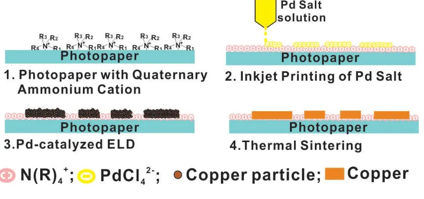
Fig. 1 schematically shows the entire process of our method, which typically includes
three steps, inkjet printing noble-metal-containing salt solution onto polyelectrolytes
modified substrate, ELD of copper and thermal sintering. Loading of noble-metal
moieties onto substrates involved a typical chemistry reaction of ion exchange, i.e., the
noble-metal moieties like PdCl42- take places of anions of Br- because of their higher
affinity to quaternary ammonium in the chain of polyelectrolytes. [25] As a
proof-of-concept, (NH4)2PdCl4 and Epson photopaper with polyelectrolytes modification were
chosen to demonstrate the process. Influence of printing parameters was thoroughly
studied and the optimum parameters such as jetting voltage control waveform, drop
space, jetting frequency and meniscus vacuum were obtained. As a result, functional
copper patterns with conductivity up to 3.9 x 10⁷ S/m (65% of bulk copper) and a feature
dimension down to 50 μm were successfully fabricated. No extreme condition was
needed and all processing steps were conducted under regular laboratory conditions.
Figure 1: Schematic illustration of paper-based metal patterns with high resolution
and conductivity via printing catalyst and subsequent ELD process.
2.2 Theory
2.2.1
Inkjet printing
Inkjet printing is a kind of technology that used for creating patterns or images by
propelling ink droplets onto different substrate, such as paper, photopaper, PET, PI,
PDMS films, etc. The idea of inkjet printing is very old and originated in the 19th century,
but was not commercialized at that time. Till 1970s, with the development of computer
and digital image technology, inkjet printer started gaining their market. Companies such
as Epson, HP, Xerox and Lexmark rose up by making inkjet printer for office use.
Several technical revolution has taken place during the past 20 year and right now there
are two main streams of printing technologies used in contemporary inkjet printer, one is
call continuous printing (CIJ) and the other is called Drop-on-demand printing (DOD).
The principle of continuous inkjet printer is shown in Fig. 2. [26] Printing ink is
pressurized by a pump (the ink supply pump) and flow from the cartridge to the nozzles.
Very small ink droplets are then jetted through the nozzle at high speed. The ejected
droplets then pass through a pair of charge electrode and are selectively charged
according to the printed image data. Charged droplets then pass through a pair of
deflection electrode where a high voltage is applied and are separated according to their
charge. After that, the charged droplets hit the substrate from bottom to top. Either the
substrate plate or the printing nozzle can move in X and Y directions, creating a
two-dimensional pattern with dot matrix on the substrate. Non-charged droplets will flow
straight to the gutter and then return as ink to the ink cartridge. Inkjet printer based on
this principle is losing its popularity these years, since it is expensive, hard to maintain
and need high level operative skills --- you need to adjust the orifice-shape and fix the
orifice in place manually sometimes.
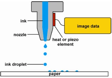
For the drop-on-demand inkjet printing technology, printers only eject droplets of ink
when they are required by the system. So a deflection system with high voltage or ink
recycling system is no longer needed. Fig. 3 shows the principle of a drop-on-demand
inkjet printhead. One of the key component on the printhead is the jetting control system
which can be divided into two kinds, the thermal inkjet and the piezoelectric inkjet. The
thermal DOD inkjet printing utilizes a heating component inside the print head used for
vaporizing some of the ink and creating a micro bubble. The formation of the bubble
which increase its volume by heating forces a drop of ink out the nozzle, realizing the
inkjet printing. While for the piezoelectric printhead, a piezoelectric membrane
(reservoir) is placed upon a small ink chamber, the deformation of the piezoelectric
membrane under different voltage will them force a drop of ink out the nozzle. By
controlling the jetting voltage value and jetting voltage waveform, the size of the droplets
can be precisely controlled, enabling a robust high resolution printing.
Figure 2: Principle of continuous inkjet printer. (Copy from [26])
Figure 3: Principle of drop-on-demand inkjet printer. (Copy from [10])
Regarding all these pros and cons, we finally chose a DOD inkjet printer as our printing
tool, for its ability of room temperature jetting, relative low cost and controllable jetting
waveform. The model we used in this project is Dimatix DMP-2800 DOD materials
printer, shown in Fig.4.
Figure 4: Dimatix DMP-2800 DOD inkjet printer used for this project.
2.2.2
Electroless deposition
Electroless deposition or electroless plating is an auto-catalytic chemical reaction used
for depositing a layer of metal, usually copper and nickel, on a solid substrate such as
metal or plastic. It is the most important process for through hole plating (THP) of printed
circuit boards (PCBs) using the indirect-conventional method. The most important
benefit of this technique is that it is not necessary to apply an electric filed/current
through the solution to make the reaction occur and in most cases the electroless
deposition can form a well deposited metal film on the substrate under room temperature.
Electroless copper deposition was first reported by Narcus [27] and more than ten years
later this technique was commercialized. [28, 29] In recent years modified formulations
have rapidly developed enabling a higher plating rate, higher plating quality and
extremely stable conditions under a wide range of plating conditions. [30-32]
2.3 Materials and experiments set-up
2.3.1
Materials
The substrate used for printing was EPSON Ultra Premium Photopaper Glossy, treated
with polyelectrolytes containing quaternary ammonium by Epson Company. Ammonium
tetrachloropalladate (II) ((NH4)2PdCl4, 97%) and anhydrous glycerol (C3H5(OH)3, 99%)
used for ink preparation were bought from SIGMA-ALDRICH and AMRESCO
respectively. Chemicals used for ELD process were copper (II) sulfate pentahydrate
(CuSO4•5H2O, 98%, SIGMA-ALDRICH), potassium sodium tartrate tetrahydrate
(C4H4KNaO6.4H2O, 99%, SIGMA-ALDRICH), formaldehyde solution (HCHO,
36.5-38% in H2O, SIGMA-ALDRICH) and Sodium Hydroxide (NaOH, 97%, CALEDON).
2.3.2
Preparation of the palladium salt ink
A glycerol-water solution with viscosity of ~11 centipoise (cp) was achieved by mixing
anhydrous glycerol and distilled water in the ratio 3:2 by volume. [33, 34] Ammonium
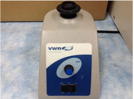
tetrachloropalladate (II) was then added, followed by four minutes mixing in the VWR
mixer (Fig.5) until a clear dark yellow solution was obtained. The optimum viscosity for
inkjetable fluids in piezoelectric Drop-on-Demand (DOD) printhead reported in literature
is 10-12 cp at room temperature. [35] Based on these, inkjet printable inks containing
different concentration of palladium ions were prepared and viscosity was measured. To
find the optimum ink for the following inkjet printing and ELD process, solutions with
different Pd salt concentration (10-60 mM) were prepared in the same way. All prepared
inks were degassed under a vacuum chamber of 2 psi for 1 hour to remove dissolved gas,
followed by filtering with a 0.2 μm springe filter to get rid of undesired particles which
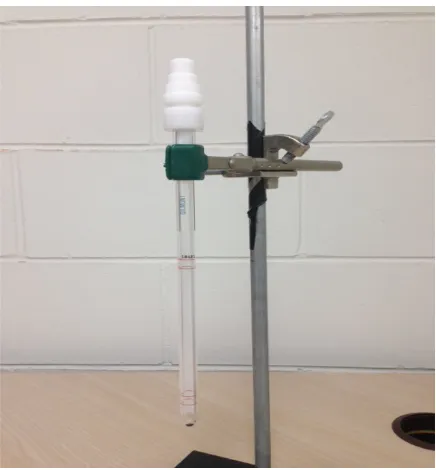
inhibits jetting. The final viscosity was measured with a Gilmont GV-2100 (Fig.6)
Falling Ball Viscometer to further confirm it was in a proper range.
Figure 5: VWR mixer
Figure 6: Gilmont GV-2100
2.3.3
Inkjet printing and parameters optimization
Printing patterns were designed and drew with vector drawing software with colour
values set to R=0, G=0, B=0 and exported as binary bmp format in bitmap colour model
with a resolution of 1300 ppi. Inkjet printing was performed using a commercially
available inkjet Dimatix DMP-2800 materials printer (FUJIFIL Dimatix, USA, Fig.4),
equipped with a 1 PL piezoelectric DOD 16-jet cartridge that can deposit features as
small as 20 μm. Two cameras were installed in the printer, the high speed side view
camera was used for monitoring the droplets in real time and the top view camera was for
checking the printed patterns and move the print head to the position where you want to
start the printing. The stage is an X-Y two directions vacuum stage with small hole-arrays
on it, enabling a vacuum absorption between the substrate and stage. Inkjet printing
experiment set up is shown in Fig.7.
Figure 7: Inner structure of the inkjet printing system (Copy from [36])
Printing parameters such as jetting period, jetting voltage control waveform, meniscus
vacuum, printhead temperature were dynamically adjusted according to the real-time
droplets video generated by a built-in high frequency camera (side view camera in Fig.7).
Epson Ultra-Premium Glossy photopaper was used as the substrate for printing and was
cut into a 10 cm x 10 cm square to reduce deformation caused by heating and wetting.
Prepared photopaper was placed on a vac-sorb substrate with temperature at 30°C and
fixed by scotch tape. Lines of the same width were printed with the drop space set to 20
µm, 25 µm, 30 µm and 35 µm respectively and examined by microscope. Results showed
a drop space of 25 µm giving the best pattern thus complex and functional patterns were
then printed with optimum settings (maximum jetting frequency 20 kHz, drop space 25
µm, meniscus vacuum 3.5 H2O, printhead temperature 30°C, printhead angle 3.6°, jetting
period 41.792 µs, jetting voltage 23.60 ± 0.4 V, printing height 150 µm, cleaning cycle of
1 s purging –1 s spitting –2 s blotting, tickle mode on with frequency 2 kHz).
2.3.4
ELD of copper and thermal sintering
ELD process was conducted to apply copper pattern onto the printed feature. The detailed
process of ELD can be found in former literatures. [18, 37, 38] Briefly, patterns printed
with inks featuring Pd salt concentration of 10 mM, 20 mM, 30 mM, 35 mM, 40 mM, 45
mM, 50 mM, 55 mM and 60 mM were put into a plating bath containing 1:1 mixture of
freshly prepared solutions I and II. Solution I consists of 13 g/L CuSO4•5H2O, 12 g/L
NaOH and 29 g/L KNaC4H4O6•4H2O which were added into distilled water in sequence.
Solution II is 9.5 mL/L HCHO in distilled water. Deposition time was controlled to 30
min, 40 min, 60 min, 120 min, and 180 min for printed patterns under the same setting.
Deposited copper lines were air dried and then put into a Fisher 1500 DEG Tube Furnace
(Fig.8) for sintering. Nitrogen was flowing for 30 minutes before heating to ensure that
no residual oxygen was in that tube. Sintering was kept for an hour under continuous
nitrogen flow at 200°C and heating rate set to 15oC/min. [39, 40]
Figure 7: Fisher 1500 DEG Tube Furnace
2.3.5
Characterization
The viscosity of the inks was measured by a Gilmont GV-2100 Falling Ball Viscometer
using a 316 stainless steel (SS) high-precision ball with a 7 mL of sample volume. Real
time images of the droplets were captured with a CORRECT PL- 4x40 built-in camera.
For studying the surface of electroless plated copper patterns before and after sintering, a
GENTAUR NJF-120A metallurgical microscope and a NOVEL Optics HDCE-90D
(3488X2616) CCD camera were used to obtain the image of the pattern. A Hitachi
S-4500 field emission scanning electron microscopy (SEM) was also used to observe the
surface morphologies of the plated patterns. Atomic force microscope (AFM, Dimension
V equipped with a Nanoscope controller V and Nanoscope software 7.30, Veeco) was
used to obtain height information. Chemical composition information of the samples was
obtained with a Kratos Axis Ultra spectrometer using a monochromatic A1 Kα radiation
source. Adhesion was determined by the use of a cross scotch tape test, following ASTM
D-3359 using 3M # 600 tape. [41] A four-probe method using M 2400 Keithley
Multimeter was carried out to measure the sheet resistance, from which conductivity was
calculated. X-ray diffraction analysis was done using Rigaku Ultima-IV XRD
goniometer.
2.4 Results and discussion
2.4.1
Ink viscosity and stability
Negatively charged tetrachloropalladate group (-PdCl42-) tends to form chemical bonds
with the positively charged quaternary amine group (NR4+-) on the photopaper. A
bivalent tetrachloropalladate group will combine with two monovalent quaternary amine
groups when the ink droplet is in contact with the photopaper substrate which results in a
strong adhesion between the palladium ions and the substrate. Rate of ELD of copper as
well as the plated copper density are proportional to the concentration of catalyst
(palladium ion in this case), thus a high concentration of the palladium salt is preferred.
[42, 43] However, the number of quaternary amine groups on the surface of photopaper is
limited, which means excessive palladium salt will result in unbonded palladium ions on
the surface. Unbonded ions will disperse on the photopaper and dissolve in deposition
solution during the process of ELD, causing serious losses in resolution (compared
experimental results are showed in Section 2.4.3-ELD of Copper). Therefore, inks with
concentrations ranging from 10 mM to 60 mM were prepared to find the optimal
solution.
Fig.8 shows that viscosity increases proportionally with concentration of ammonium
tetrachloropalladate. Yet, all prepared inks were still in the range of the optimum
requirement (10 ~ 12 cp) for printing. In order to investigate the stability of the
(NH4)2PdCl4 ink, four tubes of prepared solution (45 mM) were store in a constant 4°C
refrigerator and another four tubes (also 45 mM) were stored in a dark cabinet at room
temperature (22°C). Colour change of the inks was checked daily. UV/Vis spectrometer
measurements were taken to characterize the status of the inks and the results are shown
in Fig. 9. For inks stored at room temperature, visible precipitation was clearly observed
three days later and gradually increased with time. In order to rule out any effects of the
sediment and get a reasonable result, we filtered the ink with a 0.2 µm syringe filer each
time before the UV/Vis measurements (Fig. 9).
To get rid of the influence of the light on the stability of the inks, all prepared inks were
stored in dark. Both the fresh inks and the samples stored at 4 °C for 180 days exhibited
an absorption peak at ~390 nm originating from two transitions of the PdCl42-. [44] One
day later at room temperature, the maximum absorption peak of the solution had shifted
to ~375 nm and the absorptivity was also lightly reduced, indicating the decrement of the
PdCl42- concentration and hydration to PdCl2(H2O)2 and [PdCl(H2O)3]+. Spectra of inks
after three days showed an absorption peak at ~250 nm and a slight shift back to longer
wavelengths in lower absorption values as time increased, attributing to the formation of
[Pd(H2O)4]2+ and reduced palladium ion. The decrement of the palladium ion
concentration and the increasingly forming precipitation is probably due to the
self-oxidation-reduction reaction of the Pd ion aquo-complex which results in the increment
of relative chloride concentration, leading to the formation of [PdCl(H2O)3]+ and
PdCl2(H2O)2. The palladium salt solutions after standing up to 180 days at 4°C showed
no precipitation or deterioration. The colour of the ink is still dark yellow just as that of
the initial solution. The ink remained stable under 4°C for more than 180 days without
observation of sediment and also showed its capability of producing successful printing
results. Inks stored under room temperature after 30 days still showed its ability to trigger
the ELD process, but the ELD process was in a very low rate, usually taking more than
three hours to complete and the deposited patterns were no longer uniform and
continuous, indicating that such inks were no longer suitable for making a high resolution
functional circuits. Thus, all the inks used for final printing were either fresh made or
those stored at 4°C.
Figure 8: Viscosity of inks with different Pd salt concentration
Figure 9: UV/visible-spectra (fitted) results of freshly prepared palladium (II) salt
ink (triangle facing down) and inks after storage at room temperature for 8 hours
(triangle facing up), 3 days (round circle), 180 days (square) and 180 days stored
under 4 °C (diamond)
2.4.2
Inkjet printing of salt solution
The cartridge of ink jetting devices is always operated under negative pressure to keep
the meniscus at the edge of the nozzle and prevent the ink from dripping under the action
of gravity. The pressure difference between the inside and outside of the cartridge, which
is also known as the meniscus vacuum, needs to be adjusted depending on the viscosity
and surface tension of the ink. To obtain the optimum meniscus vacuum level, a built-in
camera was used to monitor the formation of droplets in real time. Meniscus vacuum
level was set to 3.2, 3.3, 3.5, 3.8 and 4.0 (inches of water) and under each level the
printhead continuously worked for ten minutes. Results showed that a meniscus vacuum
of 3.5 H2O gave the most stable and reliable ejected droplets. Leakage was observed on
some of the nozzles when the vacuum level was lower than 3.5 H2O. Sate of the ink
droplets under different jetting parameters is shown in Fig.10 ((a) Misdirected jetting
caused by accumulated leaked ink around the nozzle. (b) Satellite droplets caused by
relative high jetting voltage. (c) Droplets after applying the optimum parameters
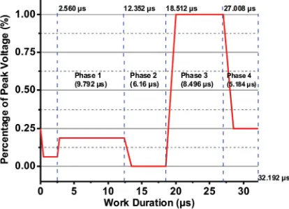
(meniscus vacuum: 3.5 H2O, jetting voltage peak ~24.30 V, single jetting duration:
32.192 µs (phase 1: 9.792 µs, phase 2: 6.160 µs, phase 3: 8.496 µs, phase 4: 5.184 µs),
maximum jetting frequency: 20 kHz)) The leaked ink attached and accumulated around
the nozzle, causing misdirected jetting and blocked nozzle Fig. 10a. For the vacuum level
higher than 3.5 H2O, a relative high voltage (~28 V) must be applied to the nozzle in
order to overcome the excessive negative pressure to make it jet. However, the increased
voltage results in the breakup of the liquid ligament and large deformation of the piezo
membrane which consequently leads to the generation of a primary drop and one or
several satellite droplets (Fig. 10b). [21] Typically, the satellite droplets may cause
undesired patterns and a serious loss in resolution, and therefore should be avoided as
much as possible. For the piezoelectric printhead, the velocity of droplet ejected from the
nozzle is a function of applied peak voltage. We observed that the distance (from the
nozzle plate to the place where droplet fully formed) travelled by the droplet also
increased with the applied voltage. Higher voltage results in a bigger dot diameter
because of the increased ink droplet’s mass and velocity, which means a reduction in the
printed resolution. By applying a meniscus vacuum of 3.5 H2O, the optimum jetting
voltage peak for the palladium ink was found to be ~24.3 V using the same real-time
monitoring method. Fig. 10c shows the images of the perfect droplets ejected from the
nozzle after applying the optimum parameters.
Nozzle clog was observed sometimes during real-time monitor, which was unacceptable
for a high resolution printing. Since all the inks were degased and filtered by a 0.2 µm
syringe filter, clogging should not be caused by undesired large particles or bubbles in the
ink. Thus, the great possibility may reside in the voltage waveform used for controlling
the bimorph on each nozzle. The bimorph is slightly deflected so that the fluid chamber
above the nozzle is depressed by a bias voltage. Typically, the voltage waveform is
divided into four segments, and each segment has three properties: slew rate, duration
and level. [45] The first segment is called the loading work during which a decreased
voltage is applied to the bimorph at the beginning of the jetting, bringing the bimorph
back to a relaxed position with the chamber at its maximum volume. However, for the
palladium salt ink the loading work segment will lead to the generation of micro-bubbles
in the nozzle, prohibiting formation of droplets since the nozzle works in a high jetting
frequency up to 20 kHz. Effect of such micro-bubbles is magnified in a nozzle with a
diameter of only 10 micron. Thus, we reduced the decreased level of the first phase, and
got the optimum jetting waveform shown in Fig. 11. A reduced level (~ 50% of the initial
one) of jetting voltage was applied to phase one, so as a longer duration of 2.550 µs, to
prevent the generation of micro-bubbles. A dampening segment was applied to phase
four to prevent the nozzles from sucking air back in and get prepared for the next
ejection. A video of the nozzles’ jetting with the optimum jetting waveform, meniscus
vacuum value (3.5 H2O) and jetting voltage peak (~ 24.30 V) was take, showing a well
alignment, stable jetting (please refer to the support information). No clog or misdirected
jetting occurred during continuous working for one hour, revealing a robust and
high-resolution printing with ammonium tetrachloropalladate (II) solution was achieved.
Figure 10: Droplets pictures under different jetting conditions (a) Misdirected
jetting caused by accumulated leaked ink around the nozzle. (b) Satellite droplets
caused by relative high jetting voltage. (c) Droplets after applying the optimum
parameters (meniscus vacuum: 3.5 H2O, jetting voltage peak ~24.30 V, single jetting
duration: 32.192 µs (phase 1: 9.792 µs, phase 2: 6.160 µs, phase 3: 8.496 µs, phase 4:
5.184 µs), maximum jetting frequency: 20 kHz).
Figure 11: Modified waveform for the ammonium tetrachloropalladate (II) ink
2.4.3
ELD and conductivity
ELD of copper was conducted under ambient environment, showing a satisfied
deposition rate. Table 1 shows the deposition results of patterns printed with inks of
different concentration. Patterns used for testing were 3 mm x 3 mm squares, printed
under the same condition with inks at different concentration.
Table 1: ELD of copper results of patterns printed with different concentration
(Scale bar: 1 cm)
Sample No.
PdCl42-
Concentration Time Results
1 10 mM 3 hours No copper
2 20 mM 3 hours No copper
·3 30 mM 2 hours
4 35 mM 2 hours
5 40 mM 1 hour
6 45 mM 40 mins
7 50 mM 40 mins
8 55 mM 30 mins
9 60 mM 30 mins
Patterns were taken out of the deposition solution when no observable changes happened
to their surfaces. Deposition time is 3~4 times longer than conventional ELD which
usually happens on a PET or PI substrate. This may result from a smaller surface area of
the reactive ions and a less active catalyst newly formed on the photopaper. The colour of
the photopaper substrate after ELD process changed in different degrees, the longer the
ELD process, the greater the colour changed. Two hours ELD made the colour of group
#3, #4 changed from white to a little bit green, while for group #5 - #9 which the time of
ELD process was controlled down to less than one hour, the photopaper still kept its
white colour but became a little bit grey. No crack or damage was observed on the
substrate of all ELD process time. Table 1 group #1 and #2 show that a concentration
below 20 mM is not able to trigger the deposition, a relative long deposition time is
![Figure 2: Principle of continuous inkjet printer. (Copy from [26])](https://thumb-us.123doks.com/thumbv2/123dok_us/7794373.1292635/33.612.120.545.151.507/figure-principle-continuous-inkjet-printer-copy.webp)
![Figure 7: Inner structure of the inkjet printing system (Copy from [36])](https://thumb-us.123doks.com/thumbv2/123dok_us/7794373.1292635/38.612.110.533.71.313/figure-inner-structure-inkjet-printing-copy.webp)