Design and Implementation of ALU Using Reversible Decoder Logic
Y. Jyosthna1, B. venkatesu2
1M.tech student, ECE department, Shree Institute of Technological Education, Peddanjimedu, Andhra Pradesh, India
2Assistant professor, ECE department, Shree Institute of Technological Education, Peddanjimedu, Andhra Pradesh, India
ABSTRACT
Digital system implemented by using conventional gates or irreversible logics like AND and OR gates dissipates a major amount of energy in the form of bits which gets erased during logical operations. This problem of energy loss can be solving by using reversible logic circuits in place of conventional circuits. The Irreversible logic is replaced by reversible logic to decrease the Power dissipation. Reversible logic functions have emerged as an important research area. Implementing the reversible logic has the advantages of reducing gate counts, garbage outputs as well as constant inputs. In today’s world ALU is one of the very important part of any system having many applications in computers, cell phones, etc. Addition, subtraction operations are realized using reversible by using reversible gates. Reversible decoder is designed using Fredkin gates with minimum Quantum cost.. The proposed method require less complexity, less hardware, minimum number of gates, minimum number of garbage inputs and minimum number of constant inputs than existing methods. The proposed circuits will be simulated using ModelSim simulator and implemented in Xilinx.
Keywords : Reversible Logic, Quantum Computing, Garbage Outputs, Full Adder, Full Subtractor, Decoder.
I.
INTRODUCTIONToday’s new technology offers faster, smaller and complex circuits. Moore’s law states that Performance (speed) of an integrated circuit per unit cost increased by a factor two for every 18 months. In order to achieve higher speed the clock frequency must be high and for smaller, complex circuit’s the number of transistors in the IC must be large and they are more closely packed in order to save area. As the IC will be faster, complex means that will increases the power dissipation in the circuit. Almost all conventional computers comprises of million numbers of gates that are irreversible in nature. During logical operations in the circuit some information is erased or lost that will causes heat dissipation and energy loss.
on the present input unlike sequential circuits in between input vectors and output vectors. And they can be made to run backward direction also. Certain limitations are to be considered when designing circuits based on reversible logic (i) Fan out is not permitted in reversible logic and (ii) Feedback is also not permitted in reversible logic. In Reversible logic using outputs we can obtain full knowledge of inputs. Reversible logic conserves information. Some cost metrics like Garbage outputs, Number of gates, Quantum cost, constantinputs are used to estimate the performance of reversible circuits. Garbage outputs are the extra outputs which help to make inputs and outputs equal in order to maintain reversibility. They are kept alone without performing any operations. Number of gates count is not a good metric since more number of gates can be taken together to form a new gate. Quantum Cost is the number of elementary or primitive gates needed to implement the gate. It is nothing but the number of reversible gates (1×1 or 2×2) required to construct the circuit. Delay is one of the important cost metrics. A Reversible circuit design can be modeled as sequence of discrete time slices and depth is summation of total time slices. In Digital Electronics the binary decoder is a combinational logic circuit that converts the binary integer value to the associated output pattern.
II.
REVERSIBLE LOGICSReversible Gates are the circuits in which number of outputs is equal to the number of inputs and there is a one to one mapping between the vector of inputs function. In certain cases these become mandatory to attain reversibility. The output that is added to an n x k function to make it reversible is called as garbage output.
The following simple formula shows the relation between constant inputs and garbage outputs :
(Input + Constant inputs) = (Output + Garbage Outputs).
Quantum Cost
Quantum cost may be defined as the cost of the circuit in terms of the cost of a primitive gate. It is calculated by the number of primitive reversible logic gates (1*1 or 2*2) required to realize the circuit. The quantum cost of a circuit is the minimum number of 2*2 unitary gates to represent the circuit keeping the output unchanged. The quantum cost of a 1*1 gate is 0 and that of any 2*2 gate is the same, which is 1.
Basic Reversible Logic Gates
Some of the important reversible logic gates are: NOT Gate, Feynman Gate, Toffoli gate, Fredkin Gate as give below.
NOT Gate:
Feynman Gate:
Figure below shows The Feynman gate which is a 2*2 gate and is also called as Controlled NOT and it is widely used for fan-out purposes. The inputs (A, B) and outputs P=A, Q= A XOR B. It has quantum cost one.
Toffoli Gate:
Figure below shows a 3*3 Toffoli gate. The input vector is I (A, B, C) and the output vector is O (P, Q, R). The outputs are defined by P=A, Q=B, R=AB XOR C Quantum cost of a Toffoli gate is 5
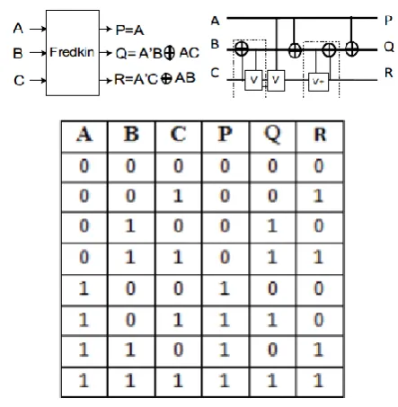
Fredkin Gate:
Figure below shows a 3*3 Fredkin gate. The input vector is I (A, B, C) and the output vector is O (P, Q, R). The outputs are defined by P=A, Q=A′BAC and R=A′C AB. Quantum cost of a Fredkin gate is 5
TR Gate:
TR Gate is a 3×3 reversible gate. The outputs are defined as shown in the below figure. The quantum cost of TRG gate is given by 4.
PERES GATE (PG):
Figure 1. Peres Gate and its Truth Table
III.
RELATED WORK
Reversible decoder:
Different Reversible Decoder circuits like 2×4, 3×8, 4×16 are designed using Fredkin Gates (mainly), Feynman gates and Peres gate. Some combinational circuits like comparator adder, subtractor, multiplexers etc., are designed using these decoders. The concept of duplicating a single output to required number of outputs using Feynman gate is introduced where Fan-out was not allowed in reversible computation.
A. Design and operation of proposed 2:4 decoder If x and y are the inputs to the decoder, then the four outputs will be xy, x’y, xy’ and x‘y’. The proposed design uses Peres Gate, TR Gate and CNOT Gate as shown in Fig 1. The Peres gate gives outputs x ^ y, and xy. It is notable that. ( ) A NOT gate is used to flip the output (x^y) which does not increase the quantum cost. Similarly the TR gate gives outputs x^y and xy’ and the XOR of these two gives x ‘y. So simply by using three more CNOT gates, all four outputs are available. The total quantum cost of this design is 11, since Peres Gate and TR gate both have quantum cost 4 and CNOT gate costs 1.
Figure 2.1. 2:4 decoder using Peres, TR and CNOT gates.
B. Design of 3:8 decoders
Henceforth, we shall call the 2:4 decoder as decoder block having two inputs and four outputs. A 3:8 decoder has the outputsx‘y‘z’; x‘y‘z; xy‘z‘; xy‘z; x‘yz‘; x‘yz; xyz’; xyz. So every output of the 2:4 decoder needs to be multiplied twice, once with z0 and then with z. To achieve this using Peres or TR gate, there will be need of a single gate for each multiplication resulting in 8 gates with a quantum cost of 32 and 16 garbage outputs (2 for each gate). A better model will be to use Fredkin gate for higher dimension. Each Fredkin gate is capable of performing two multiplications thus reducing the number of gates to 4 and garbage outputs to 1. The architecture is shown in Fig.2.
Figure 2.2. 3:8 decoder using 2:4 decoder block and Fredkin Gates.
C. 4 To 16 Decoder Design
existing method the author has given a novel design of 4x16 decoder whose Quantum Cost is less than the previous design. Replacing fredkin gates for designing 2×4 decoder reversible gates like peres gate, TR gate, NOT gate and CNOT gate are used as shown in figure9.The whole design is done using Fredkin, CNOT, Peres gates which give better Quantum Cost when compared to the other reversible Logic gates. The number of gates required to design4x16 decoder are 18 in which there are 12 fredkin gates, one peres gate, one TR gate, one NOT gate and 3 CNOT gates. The sum of all the quantum costs of each gate gives total quantum cost of 4x16 decoder.
Figure 3. Circuit diagram of Reversible 4×16 decoder
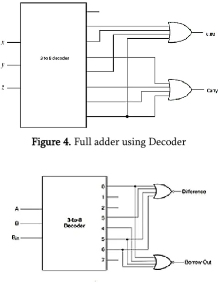
D. Full Adder/ Subtractor
For designing a full adder a 3 to 8 decoder and two four input OR gates are required. The min terms for SUM and CARRY are derived from output pattern of decoder. Similarly the full subtractor was also designed.
Equation for sum S= ∑ (1, 2, 4, 7) Equation for carry C= ∑ (3, 5, 6, 7) Equation for difference D= ∑ (1, 2, 4, 7) Equation for borrow B= ∑ (1, 2, 3, 7)
In the above min term expressions we can observe that the same min term output of decoder drives sum and carry outputs of full adder ( i.e., out[7] of decoder output pattern). Since Fan-out is not allowed in reversible logic, the Feynman gate is used to
duplicate outputs. Similarly for full subtractor outputs of decoder (i.e., out[1], out[2] and out[7]) are duplicated. By using this full adder a 4 bit full adder/subtractor is designed. The simulated output is shown in figure15. To design 4-bit full adder/subtractor circuit four full adders are required. The Cin input drives the first full adder. If Cin is given with low input4-bit addition is performed and if Cin is given with high input the 4-bit subtraction in the form of 1’s complement addition is performed.
Figure 4. Full adder using Decoder
Figure 5. Full subtractor using decoder
IV.
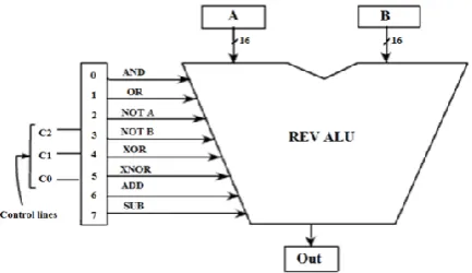
PROPOSED METHODProposed ALU Design
For instance, if contribution to control unit is 000, the decoded bits will be 10000000 and in the wake of accepting the direction bits from the decoder AND operation is performed by ALU as indicated by the operands from Register A and Register B. Block diagram of the ALU is shown below fig.
Figure 6. 16 bit reversible ALU.
V.
RESULTSBlock Diagram of reversible ALU:
Figure 7
RTL schematic:
Figure 8
Technology schematic:
Figure 9 Simulation results:
Delay: model which can be operated as reversible ALU using reversible decoder of full adder as well as full subtractor with better performance. In this paper, different combinational circuits like fulladder, full subtractor, multiplexer, comparator circuits constructed using reversible decoder are designed. The reversible logic concept work efficiently if number of garbage outputs, constant inputs and quantum cost is low. The power dissipation is zero if the reversible logic circuits are implemented with quantum gates. If we do that then we can save power, money as well as nature.
VII.
REFERENCES
[1]. R. Landauer, "Irreversibility and Heat Generation in the Computational Process", IBM Journal of Research and Development, 5, pp. 183- 191,1961.
[2]. C.H. Bennett, "Logical Reversibility of Computation", IBM J.Researchand Development, pp. 525-532, November 1973. [3]. C H Bennett, "Notes on the History of
Reversible Computation", IBM Journal of Research and Development,vol. 32, pp. 16-23, 1998.
[4]. R. Feynman,"quantum mechanical computers:, Optic News, vol. 11,pp11-20, 1985.
[5]. William C. Athas, Lars "J" ,Svensson, Jeffrey G. koller, NestorasTzartzanis, and Eric Ying – Chin Chou, "Low-power Digital Systemsbased on Adiabatic-Switching principle", IEEE Transactions on VLSIsystems, Vol. 2, No. 4, December 1994.
[6]. A. Peres, "Reversible logic and quantum computers",phys.rev.A,Gen.Phys., vol. 32, no. 6, pp. 32663276, Dec. 1985.
[7]. H.G Rangaraju, U. Venugopal, K.N. Muralidhara, K. B. Raja,"Lowpower reversible
parallel binary
adder/subtractor"arXiv.org/1009.6218,2010. [8]. J.M. Rabaey and M. Pedram, "Low Power
Design Methodologies,"Kluwer Academic Publisher, 1997.
[9]. T. Toffoli., "Reversible Computing", Tech memo MIT/LCS/TM-151,MIT Lab for Computer Science 1980.
[10]. E. Fredkin and T. Toffoli, "Conservative logic," Int’l J.TheoreticalPhysics, Vol. 21, pp.219–253, 1982.
[11]. Y. Syamala, and A. V. N. Tilak, "Reversible Arithmetic Logic Unit",Electronics Computer Technology (ICECT), 2011 3rd International, vol.5, pp.207-211,07 july 2011.
[12]. Thapliyal H, Ranganathan N.," Design of Reversible Latches Optimizedfor Quantum Cost, Delay and Garbage Outputs" Centre for VLSI andEmbedded .
[14]. Vivek V. Shende, Aditya K. Prasad, Igor L. Markov, and John P.Hayes," Synthesis of Reversible Logic Circuits", IEEE Transaction oncomputer-aided design of integrated circuits and systems, vol. 22, No. 6,June 2003.
[15]. Payal Garg, Sandeep Saini,"A novel design of compact reversible SGgate and its applications",2014 14th International Symposium on Communications and Information Technologies(ISCIT), Sept
2014,pages 400-403, doi:
10.1109/ISCIT.2014.7011941
[16]. Jadav Chandra as, Debashis De and Tapatosh