A computational study on the variation of Bandgap due to native defects in
non-stoichiometric NiO and Pd, Pt doping in stoichiometric NiO
Srikanth Itapu1, Vamsi Borra2, and Faramarz Mossayebi3
1Department of Electronics and Communication Engineering, CVR College of Engineering,
Hyderabad, India 501510
2Department of Applied Engineering and Technology, California University of Pennsylvania,
Pennsylvania, U.S.A. 15419
3Department of Electrical and Computer Engineering, Youngstown State University,
Youngstown, Ohio, U.S.A. 44555
Corresponding E-mail: sitapu@rockets.utoledo.edu
Abstract
This paper presents computational study of non-stoichiometric nickel oxide in a 32-cell NiO system to model and validate localized heating effects due to nanosecond laser irradiation. Variation in Bandgap of NiO is studied as a function of varying concentrations of native defects ranging from 0 to 25%. It is observed that there is a slight increase in the bandgap from 3.8eV for stiochiometric NiO to 3.86eV for Ni-rich NiO and to 3.95eV for O-rich NiO. It is hence deduced that the experimental laser irradiation leads to simultaneous reduction of Ni2+ ions and oxidation of NiO as the
number of laser pulses increase. As well, a detailed study on the effects of doping nickel family elements, i.e. palladium (Pd) and platinum (Pt) in stoichiometric NiO is presented. A bandgap decrease from 3.8eV for pure NiO to 2.5eV for Pd-doping and 2eV for Pt-doping for varying doping concentrations ranging from 0-25% Pd, Pt respectively is observed.
1. Introduction
Transition metal oxides (TMOs) constitute an important section of semiconducting materials exhibiting a variety of electronic and magnetic properties that are observed with the nature of their outer d states. Point defects in TM oxides such as vacancies and interstitials play a crucial role in determining the behavior of such oxides.Nickel Oxide (NiO) is a classic example of the transition metal oxides (TMOs) that has presented significant challenges for an accurate theoretical description of their electronic structure. Due to the complicated nature of its electronic properties, NiO has received considerable attention from both experimentalists and theorists.
Density functionaltheory (DFT) study on undoped NiO was first reported in detail in [1], wherein, the electron correlations in the 3d shell of metal ions in nickel oxide were computed using a combination of local spin density approximation (LSDA) and unrestricted Hartree-Fockapproximation (U) techniques. This method was able to calculate total energy of crystalline nickel oxide and validate the obtained results by measuring the electron energy loss spectra. The local-density approximation (LDA) plus Hubbard model were implemented in [2] to compute the insulating antiferromagnetic ground state of NiO and its optical properties. It is observed that charge transfer was a result of enhancement of O 2p character at the top of the valence state rather than Ni d-d LSDA-type band gap. In [3], an ab initio study of NiO at the Pd (100) surface was studied and observed that a Ni3O4 phase existed with rhombic distribution of Ni vacancies.
A preferential formation due to surface reaction of O and NiO was shown to be thermodynamically possible along with some peculiar aspects resulting from a strong bond formation between Pd and O. In [4], magnetism of uniform amorphous NiO showed a disordered structure with a dominant antiferromagnetic coupling, an ordering temperature of 3.K, and a paramagnetic ordering temperature of -13K. NiO clusters with a size of less than 1nm indicated ferromagnetic interactions. The stability and magnetism associated with vacancy in NiO is studied using GGA+U in [5]. The role of oxygen vacancies and mechanism of oxide reduction were dealt with in [6] and the electronic structure of oxygen and nickel vacancies at the surface of NiO (100) was investigated in [7] using hybrid DFT calculations. General gradient approximation (GGA) technique was used to study the defect formation energies under different conditions and inducted magnetism by vacancies in [8]. The results indicated that the predominant defect is Ni vacancy under oxygen-rich condition and the most suitable ionization state varies with different fermi level.
The stoichiometric NiO is a Mott insulator with conductivity of 10-13 S/cm, while
nonstoichiometric NiOx is a wide-band-gap p-type semiconductor. The p-type conductivity of
NiOx originates from two positive charge compensation which favors Ni2+ vacancies [8]. Several
not well-defined in NiO films with high oxygen content [23]. From [25], [26], it is observed that high energy laser irradiation causes a change in the chemical composition as well as the electrical properties of NiO, but a thorough computational analysis hasn’t been presented till date. Due to its uncertain mechanism, nickel vacancy and/or interstitial oxygen are used to explain the electrical properties of the NiO films. To facilitate this study, density functional theory offers the right platform for defect analysis.
Also, recent studies indicate an enormous work in doped NiO to enhance room temperature ferromagnetism for multiferroic devices [27], supercapacitor applications [28] and resistive switching [29]. Dopants such Cu [29], Li [30] enhance the p-type conductivity of NiO films and have been studied extensively, both theoretically and experimentally. Doping NiO with metals in the nickel family, i.e. Palladium (Pd) and Platinum (Pt)have gained attention owing to their Electrochromic, supercapacitor and gas-sensing applications and studied extensively experimentally[31],[32],[33],[34],[35],[36],[37],[38], but no theoretical analysis has been investigated in knowing the vacancy and interstitial behavior in doped NiO. In this paper,wealso study the effect of doping Pd and Pton the bandgap of NiOby varying doping concentrations from 0 to 25% doping in a 32 cell NiO.
2. Computational method
32 cell NiO with varying concentrations from 0-25%, i.e., introducing 0 to 8 Ni or O interstitials respectively.
3. Results and discussion
Pure nickel oxide belongs to the space group Fm-3m with the space number 225. The primitive cell of NiO consists of a Ni16O16 unit of 32 atoms in a rock-salt structure. Positions of
the 32 atom basis in this cell are obtained from International tables for crystallography. The N atoms forming the fcc lattice occupy the Wyckoff position 4a.For a crystal, whose lattice reacts as an elastic medium, the Vegard law is obeyed, i.e., change of the lattice constant is proportional to the concentration of the dopant and to the difference between ionic radii of the dopant and substituted host atom. Therefore, to examine the influence of doping on the lattice constant is examined, it is important to know the concentration of native defects.
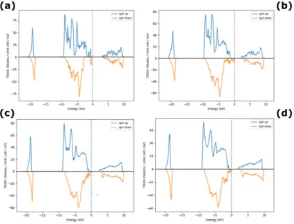
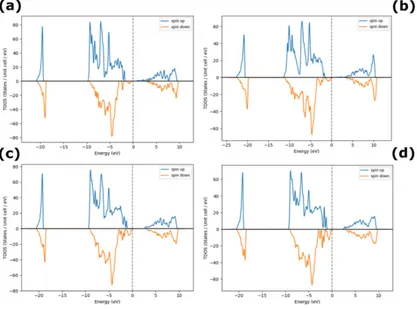
3.1 Density of states (DOS)–excess Ni occupying interstitial sites in NiO
From the GGA calculations, Ni interstitials dominate under excess Ni conditions, as depicted in
Figure 1(a-d), in agreement with the observed Ni deficiency and n-type behavior of NiO. The
results show that O interstitials are generally unstable and that O vacancies are the lowest energy
defects near the Fermi level. As a result, from [26], it is observed experimentally that, Ni-rich
NiO is typically n-type semiconductor. There is also a slight increase in the bandgap for
increasing % doping of excess of Ni in NiO system (figure 1(a-d)). Table 1 summarizes the
Figure 1. Density of States for excess Ni in NiO (a) 3%, (b) 12%, (c) 18% and (d) 25% Ni.
Table 1. Bandgap of excess Ni in NiO with respect to % doping
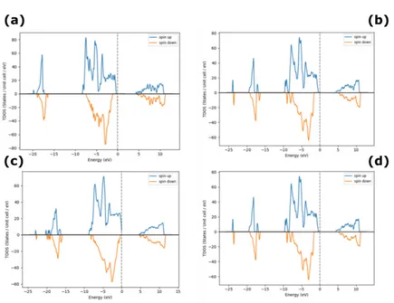
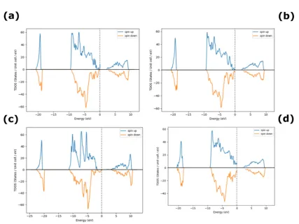
3.2. Density of states (DOS) – excess O occupying interstitial sites in NiO
The computational analysis, shown in Figure 2(a-d), reveals that, Ni vacancies dominate under
excess O conditions, which is usually the case with sputtered NiO films and is in agreement with
the observed Ni deficiency and p-type behavior of NiO. From [26], it is observed experimentally
that, O-rich NiO is typically p-type semiconductor. Table 2 depicts the increasing trend in
bandgap with an increase in O concentration.
% excess Ni 3 12 18 25
Figure 2. Density of States for excess O in NiO (a) 3%, (b) 12%, (c) 18% and (d) 25% O.
Table 2. Bandgap of excess O in NiO with respect to % doping
% excess O 3 12 18 25
Bandgap (eV) 3.80 3.85 3.90 4.00
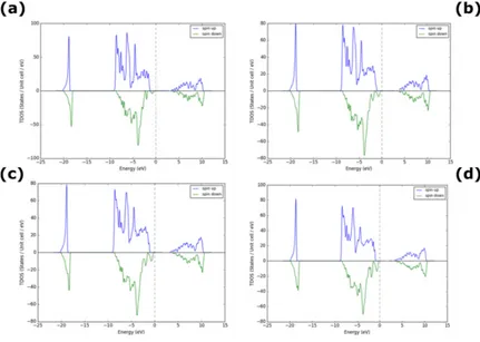
3.3. Density of states (DOS) - Pd as dopant occupying interstitial sites in NiO
Figure 3. Density of States for Pd- doped NiO (a) 3% (b) 6% (c) 9% and (d) 12% Pd.
Table 3. Bandgap of Pd –doped NiO with respect to % doping
% Pd doping 3 6 9 12 15 18 21 25
Bandgap (eV) 3.80 3.75 3.50 3.20 2.95 2.80 2.70 2.50
For higher doping percentage of Pd in NiO (fig. 4(a-d)), there is a further decrease in the bandgap of Pd doped NiO from 2.95eV to 2.5eV. This arises from the Pd2+ substituting Ni2+ sites
Figure 4. Density of States for Pd- doped NiO (a) 15%, (b) 18%, (c) 21% and (d) 25% Pd.
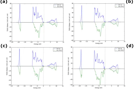
3.4. Density of states (DOS) - Pt as dopant occupying interstitial sites in NiO
Density of States for various % doping of Pt in NiO is shown in Figure 5(a-d). A band gap of 2.5eV is observed for 3 % Pd doping. It can be observed that as the doping increases, there is a slight change in the bandgap of Pd-doped NiOupto 12 % doping. Due to the large size of Pt atom, there is some amount of distortion in the lattice arrangement resulting in a dominant Pt3+
Figure 5. Density of States for Pt- doped NiO (a) 3% Pt, (b) 6% Pt, (c) 9% Pt and (d) 12% Pt.
For higher doping percentage of Pt in NiO, there is a further decrease in the bandgap of Pt doped
NiO from 2.5 eV to 2.0 eV, as shown in Figure 6(a-d). This arises from the Pd2+ substituting Ni3+
sites resulting in an increase in the lattice constant and overall volume of the cubic cell. Table 4
Figure 6. Density of States for Pt- doped NiO (a) 15%, (b) 18%, (c) 21% and(d) 25% Pt.
Table 4. Bandgap of Pt –doped NiO with respect to % doping
% Pt doping 3 6 9 12 15 18 21 25
Bandgap (eV) 2.50 2.40 2.40 2.25 2.15 2.10 2.0 2.0
4. Conclusion
for 25% Pd doping. Similarly, there is a decrease in bandgap to 2eV for 25% Pt doping. The density of state calculations suggests that, both Pd- and Pt- doped NiO are p-type in nature.
Acknowledgements
The authors would like to thank the facilities in the College of Engineering and College of
Natural Science and Mathematics at the University of Toledo to carry out this work.
REFERENCES
[1] S. L. Dudarev, G. A. Botton, S. Y. Savrasov, C. J. Humphreys, and A. P. Sutton,
“Electron-energy-loss spectra and the structural stability of nickel oxide: An LSDA+U study,” Phys. Rev. B, vol. 57, no. 3, pp. 1505–1509, Jan. 1998.
[2] O. Bengone, M. Alouani, P. Blöchl, and J. Hugel, “Implementation of the projector augmented-wave LDA+U method: Application to the electronic structure of NiO,” Phys. Rev. B, vol. 62, no. 24, pp. 16392–16401, Dec. 2000.
[3] *,† Anna Maria Ferrari, † and Mauro Ferrero, and ‡ Cesare Pisani†, “An ab Initio Periodic Study of NiO Supported at the Pd(100) Surface. Part 2: The Nonstoichiometric Ni3O4 Phase,” 2006.
[4] J. B. Yi, J. Ding, Y. P. Feng, G. W. Peng, G. M. Chow, Y. Kawazoe, B. H. Liu, J. H. Yin, and S. Thongmee, “Size-dependent magnetism and spin-glass behavior of amorphous NiO bulk, clusters, and nanocrystals: Experiments and first-principles calculations,” Phys. Rev. B, vol. 76, no. 22, p. 224402, Dec. 2007.
[5] W.-B. Zhang, N. Yu, W.-Y. Yu, and B.-Y. Tang, “Stability and magnetism of vacancy in NiO: A GGA+U study,” Eur. Phys. J. B, vol. 64, no. 2, pp. 153–158, Jul. 2008.
[7] *,† José A. Rodriguez, † Jonathan C. Hanson, ‡ Anatoly I. Frenkel, † and Jae Y. Kim, and M. Pérez§, “Experimental and Theoretical Studies on the Reaction of H2 with NiO: Role of O Vacancies and Mechanism for Oxide Reduction,” 2001.
[8] A. M. Ferrari, C. Pisani, F. Cinquini, L. Giordano, and G. Pacchioni, “Cationic and anionic vacancies on the NiO(100) surface: DFT+U and hybrid functional density functional theory calculations,” J. Chem. Phys., vol. 127, no. 17, p. 174711, Nov. 2007.
[9] J. R. Manders, S.-W. Tsang, M. J. Hartel, T.-H. Lai, S. Chen, C. M. Amb, J. R. Reynolds, and F. So, “Solution-Processed Nickel Oxide Hole Transport Layers in High Efficiency Polymer Photovoltaic Cells,” Adv. Funct. Mater., vol. 23, no. 23, pp. 2993–3001, Jun. 2013.
[10] S. C. Chen, T. Y. Kuo, and T. H. Sun, “Microstructures, electrical and optical properties of non-stoichiometric p-type nickel oxide films by radio frequency reactive sputtering,” Surf. Coatings Technol., vol. 205, pp. S236–S240, Dec. 2010.
[11] H. Sato, T. Minami, S. Takata, and T. Yamada, “Transparent conducting p-type NiO thin films prepared by magnetron sputtering,” Thin Solid Films, vol. 236, no. 1–2, pp. 27–31, Dec. 1993.
[12] H.-L. Chen, Y.-M. Lu, and W.-S. Hwang, “Characterization of sputtered NiO thin films,” Surf. Coatings Technol., vol. 198, no. 1–3, pp. 138–142, Aug. 2005.
[13] Y. A. K. Reddy, “Influence of Growth Temperature on the Properties of DC Reactive Magnetron Sputtered NiO Thin Films,” Int. J. Curr. Eng. Technol., vol. 2, no. 2, pp. 351– 357, Jan. 2013.
[14] B. Subramanian, M. Mohammed Ibrahim, K. R. Murali, V. S. Vidhya, C. Sanjeeviraja, and M. Jayachandran, “Structural, optoelectronic and electrochemical properties of nickel oxide films,” J. Mater. Sci. Mater. Electron., vol. 20, no. 10, pp. 953–957, Oct. 2009.
[15] A. Agrawal, H. R. Habibi, R. K. Agrawal, J. P. Cronin, D. M. Roberts, R.
Caron-Popowich, and C. M. Lampert, “Effect of deposition pressure on the microstructure and electrochromic properties of electron-beam-evaporated nickel oxide films,” Thin Solid Films, vol. 221, no. 1–2, pp. 239–253, Dec. 1992.
Bis-π-Cyclopentadienyl-Nickel,” Jpn. J. Appl. Phys., vol. 36, no. Part 1, No. 11, pp. 6884– 6887, Nov. 1997.
[17] B. T. Raut, S. G. Pawar, M. A. Chougule, S. Sen, and V. B. Patil, “New process for synthesis of nickel oxide thin films and their characterization,” J. Alloys Compd., vol. 509, no. 37, pp. 9065–9070, Sep. 2011.
[18] W. Guo, K. N. Hui, and K. S. Hui, “High conductivity nickel oxide thin films by a facile sol–gel method,” Mater. Lett., vol. 92, pp. 291–295, Feb. 2013.
[19] M. Tanaka, M. Mukai, Y. Fujimori, M. Kondoh, Y. Tasaka, H. Baba, and S. Usami, “Transition metal oxide films prepared by pulsed laser deposition for atomic beam detection,” Thin Solid Films, vol. 281–282, pp. 453–456, Aug. 1996.
[20] B. A. Reguig, A. Khelil, L. Cattin, M. Morsli, and J. C. Bernède, “Properties of NiO thin films deposited by intermittent spray pyrolysis process,” Appl. Surf. Sci., vol. 253, no. 9, pp. 4330–4334, Feb. 2007.
[21] J.-K. Kang and S.-W. Rhee, “Chemical vapor deposition of nickel oxide films from Ni(C5H5)2/O2,” Thin Solid Films, vol. 391, no. 1, pp. 57–61, Jul. 2001.
[22] H. Liu, W. Zheng, X. Yan, and B. Feng, “Studies on electrochromic properties of nickel oxide thin films prepared by reactive sputtering,” J. Alloys Compd., vol. 462, no. 1–2, pp. 356–361, Aug. 2008.
[23] W. Brückner, R. Kaltofen, J. Thomas, M. Hecker, M. Uhlemann, S. Oswald, D. Elefant, and C. M. Schneider, “Stress development in sputtered NiO thin films during heat treatment,” J. Appl. Phys., vol. 94, no. 8, p. 4853, 2003.
[24] A. Kuzmin, J. Purans, and A. Rodionov, “X-ray absorption spectroscopy study of the Ni K edge in magnetron-sputtered nickel oxide thin films,” J. Phys. Condens. Matter, vol. 9, no. 32, pp. 6979–6993, Aug. 1997.
[25] S. Itapu, K. Khan, and D. G. Georgiev, “Effect of UV Laser Irradiation on the properties of NiO films and ZnO/NiO Heterostructures,” MRS Adv., vol. 1, no. 4, pp. 293–298, Feb. 2016.
sputtered NiO x thin films by pulsed UV laser irradiation,” Phys. status solidi, vol. 214, no. 2, p. 1600414, Feb. 2017.
[27] J. H. He, S. L. Yuan, Y. S. Yin, Z. M. Tian, P. Li, Y. Q. Wang, K. L. Liu, and C. H. Wang, “Exchange bias and the origin of room-temperature ferromagnetism in Fe-doped NiO bulk samples,” J. Appl. Phys., vol. 103, no. 2, p. 23906, Jan. 2008.
[28] D. Han, X. Jing, J. Wang, P. Yang, D. Song, and J. Liu, “Porous lanthanum doped NiO microspheres for supercapacitor application,” J. Electroanal. Chem., vol. 682, pp. 37–44, Aug. 2012.
[29] J.-C. Li, X.-Y. Hou, and Q. Cao, “Effect of Cu doping on the resistive switching of NiO thin films,” J. Appl. Phys., vol. 115, no. 16, p. 164507, Apr. 2014.
[30] T. Dutta, P. Gupta, A. Gupta, and J. Narayan, “Effect of Li doping in NiO thin films on its transparent and conducting properties and its application in heteroepitaxial p-n junctions,” J. Appl. Phys., vol. 108, no. 8, p. 83715, Oct. 2010.
[31] G. Li, L. Li, D. Jiang, and J. Shi, “Design of a meso-structured Pd/NiO catalyst for highly efficient low temperature CO oxidation under ambient conditions,” RSC Adv., vol. 5, no. 50, pp. 40352–40357, 2015.
[32] A. M. Ferrari, M. Ferrero, and C. Pisani, “An ab Initio Periodic Study of NiO Supported at the Pd(100) Surface. Part 2: The Nonstoichiometric Ni 3 O 4 Phase,” J. Phys. Chem. B,
vol. 110, no. 15, pp. 7918–7927, Apr. 2006.
[33] M. Sambi, R. Sensolo, G. A. Rizzi, M. Petukhov, and G. Granozzi, “Growth of NiO ultrathin films on Pd(100) by post-oxidation of Ni films: the effect of pre-adsorbed oxygen,” Surf. Sci., vol. 537, no. 1–3, pp. 36–54, Jul. 2003.
[34] X. Zou, Z. Rui, and H. Ji, “Core–Shell NiO@PdO Nanoparticles Supported on Alumina as an Advanced Catalyst for Methane Oxidation,” ACS Catal., vol. 7, no. 3, pp. 1615–1625, Mar. 2017.
[36] L. Nie, A. Meng, F. Teng, and B. Cheng, “Hierarchically macro-mesoporous flowerlike Pt/NiO composite microspheres for efficient formaldehyde oxidation at room
temperature,” RSC Adv., vol. 5, no. 102, pp. 83997–84003, 2015.
[37] L. Qi, B. Cheng, W. Ho, G. Liu, and J. Yu, “Hierarchical Pt/NiO Hollow Microspheres with Enhanced Catalytic Performance,” ChemNanoMat, vol. 1, no. 1, pp. 58–67, May 2015.
[38] M. Walker, C. R. Parkinson, M. Draxler, M. G. Brown, and C. F. Mcconville, “Initial growth of platinum on oxygen-covered Ni(1 1 0) surfaces,” 2006.
[39] G. Kresse and J. Furthmüller, “Efficient iterative schemes for ab initio total-energy calculations using a plane-wave basis set,” Phys. Rev. B, vol. 54, no. 16, pp. 11169– 11186, Oct. 1996.
[40] G. Kresse Av and J. Furthmiiller, “Efficiency of ab-initio total energy calculations for metals and semiconductors using a plane-wave basis set,” Comput. Mater. Sci., vol. 6, pp. 15–50, 1996.