ASIC Implementation of Multiplexer Based
DAA
D.Srimathi1, P.Santhini2, M.Malarvizhi3, B.SahayaJenila4
PG Student [Applied Electronics],Department ofECE, IFET college of Engineering, Villupuram, Tamilnadu,
India1,2,3,4
ABSTRACT: In Digital Image Processing Point, Line and Edge detection are performed through software approach. The proposed Architecture performs these operations through hardware approach using Distributed Arithmetic. Distributed arithmetic (DA) has been widely used to implement inner product computations with fixed inputs. Conventional ROM-based DA suffers from large ROM requirements. To reduce the memory requirements, Adder based DA uses pre-defined structure for computation. But both the methods are suitable only if at least one input is constant. This project aims to implement a new Distributed Arithmetic Architecture for point detection, line detection and edge detection in DIP when both the inputs are variable. The new architecture is termed as Multiplexer based Distributed Arithmetic (MUX based DA). The proposed architecture takes the advantage of Multiplexer and DA for inner product computations when both the inputs are variable. In addition it reduces ROM requirement and complexity in constructing Adder based architecture for higher order inputs. Here, the performance of proposed Architecture with ROM based DA, Adder based DA and with multiplier based implementation are compared. The MUX based DA reduces power up to 81% and needs 40% of area as compared with multiplier based implementation.
KEYWORDS: ROM based DA,ADDER based DA,MULTIPLEXER based DA, CADENCE 180nm Technology.
I.INTRODUCTION
Distributed Arithmetic (DA) has been widely adopted for its computational efficiency in many digital signal processing applications. The most frequently used form of computation in digital signal processing is a sum of products which is dot-product or inner-product generation. DA is generally abit-serial computation operation that forms a product of two vectors in one clock cycle. The typical applications include DCT, DFT (Discrete Fourier Transform), FIR (Finite Impulse Response), and DHT (Discrete Hartley Transform) which can be found in main stream multimedia standards and telecommunication protocols. The advantage of DA is its special non multiplication mechanization which uses adder replacing multiplication and therefore simplifies the hardware implementation. The idea behind the conventional DA, called ROM based, is to replace multiplication operations by pre-computing all possible values and storing these in a ROM. The Adder based DA uses a fixed architecture which can be obtained by distributing fixed variable is used for inner product computation. The DA technique distributes arithmetic operation rather than lumps themas multipliers do. Conventional DA called ROM based DA decomposes the variable input of the inner product into bit level to generate pre-computed data.ROM based DA uses a ROM table to store the pre-computed data, which makesit regular and efficient in silicon area in VLSI implementation. However, when the size of the inner product increases the ROM area increases exponentially and becomes impractically large, even using ROM partition.
produces inner product computation with both the inputs as variable this has application in point detection, line detection and edge detection in DIP(Digital Image Processing).
II.RELATED WORK
A new hardware distributed arithmetic was implemented for high order digital filter. it was termed as reusable distributed arithmetic. It reuses the computational block much like multipliers were used to reduce the hardware complexity [1]. A hybrid adder based DA was implemented to perform discrete cosine transform algorithm based on three processors pure RAM, mixed RAM and CORDIC based RAM[2].Row column decomposition technique was used to compute the two dimensional discrete cosine and inverse cosine transform. Word-level data sharing was computed by using cyclic convolution [3].
Distributed arithmetic (DA) based array for the (1-D) any-length discrete Hartley transform (DHT). A new algorithm was used to formulate the 1-D DHT into cyclic convolution, and realized it in a DA-based array that utilizes identical ROM modules, and eliminate the accumulation loop in the processing elements (PE's)[5].
III.ROM BASED DA
An efficient technique for calculation of sum of products or vector dot product or inner product or multiplies and accumulate(MAC). MAC operation is very common in all Digital Signal Processing Algorithms. Though inner product design using multipliers and accumulator are Fast they associated cost is intolerable .when inner product computation is consider instead of using MAC, Distributed Arithmetic (DA) uses ROM that store the pre computedpartial sum of inner product .The advantages of DA are best exploited in data path circuit designing Area savings from using DA can be up to 80% and seldom less than 50% in digital signal processing hardware designs An old technique that has been revived by the wide spread use of Field Programmable Gate Arrays (FPGAs) for Digital Signal Processing (DSP) DA efficiently implements the MAC using basic building blocks (Look Up Tables) in FPGA.
DA is a bit-serial operation that computes the inner product of two vectors without needing to use multiply operations.
Figure1:Conventional ROM based DAA
Figure 2: Simulation Report for ROM based DA
Figure 2 shows the simulation report for ROM based Distributed Arithmetic.The problem with ROM based DA is that its ROM size (2L word) grows exponentially as the order L increases. As the number of inputs and the internal precision becomes large, the ROM based DA suffers from extremely large ROM requirements. To reduce the large memory requirement Adder based DA presents fixed architecture.
IV.ADDER BASED DA
Adder Based DAA decomposes the fixed coefficients instead of variable input into bit level.The adders with shiftsreplace the multipliers in the original DA algorithm.It is possible to share terms between different bit weights resulting in area saving.The adoption of adders also makes the architecture more hardware efficient.
Figure 3:Common sharing term in adder based DA.
Figure 4: Adder based DA architecture design
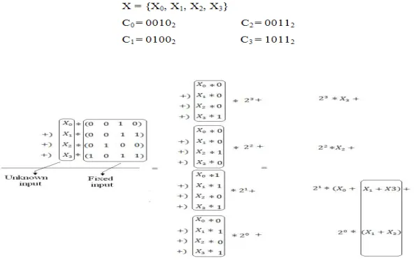
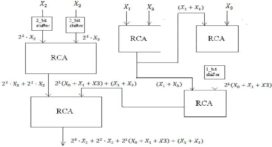
Figure 4 shows the adder based DA architecture realizing the bit-serial form of equation
The architecture consists of shifters and ripple carry adders. The shifters provide the shift needed and the ripple carry adder(RCA) tree is used to generate final inner product results.
Figure 5 shows the simulation report for adder based DA. It is complex to construct fixed architecture in Adder based DA for higher order inputs and also it perform inner product computation only when one input is fixed. This disadvantage is overcome in MUX based DA architecture.
V. MULTIPLEXER BASED DA
The advantage of Multiplexer based DA over ROM based DA and Adder based DA is that, it can perform inner product computations for two variable vectors. As per the expression both the multiplier and multiplicand are variables.
Y = a. X1 + b. X2 + c. X3 + d. X4
In MUX based DA the property of multiplexer in implementing basic logic gates is used rather than using parallel AND Gates. Implementation of AND gate using 2:1MUX
Basic expression of Multiplexer: Y= a (~s) + b(s)
Put a=0 then Y = b(s) Where ‗a‘ and‗s‘ are vector inputs.
Equation defines the AND Gate and can be used in multiplication operation by distributing one variable vector and given it to the select line through the shift register and the other vector to input 2 of MUX.
Figure 6: Multiplication of two vectors using MUX
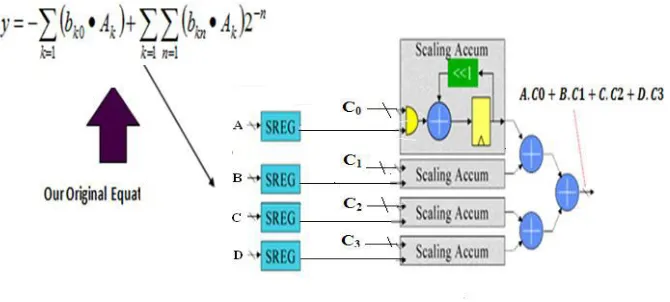
The Figure 6 shows the multiplication of two vector inputs. In most of the multiply accumulate applications in signal processing, one of the multiplicands for each product is a constant. Usually each multiplication uses a different constant. Using most compact multiplier, the scaling accumulator, it is possible to construct a multiple product term parallel multiply-accumulate function in are latively small space if it is willing to accept a serial input.
Figure 7: Implementation of original equation
If stop to consider that the scaling accumulator multiplier is really just a sum of vectors, then it becomes obvious that we can rearrange the circuit.
The adder tree combines the 1 bit partial products before they were accumulated by the scaling accumulator. After rearranging the order in which the 1xN partial products are summed. Instead of individually accumulating each partial product and then summing the results, postpone the accumulate function until after summed all the 1xN partials at a particular bit time. This simple rearrangement of the order of the adds has effectively replaced N multiplies followed by an N input add with a series of N input adds followed by a multiply. This arithmetic manipulation directly eliminates N-1 Adders in an N product term multiply-accumulate function. For larger numbers of product terms, the savings becomes significant.
Figure 8: MUX based DA architecture design
The block diagram of proposed MUX based DA architecture is shown in Figure 8.The proposed architecture takes the advantage of Multiplexer and DA for inner product computation of variable inputs.
VI. RESULT AND DISCUSSION
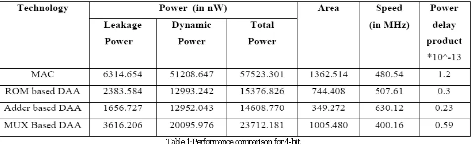
The Table 1& Table 2 compare the power, area, and speed of the ROM based DA, Adder based DA, Multiplier based implementation and MUX based DA which is synthesized using ASIC tool - Cadence.
Table 1:Performance comparison for 4-bit
Table 2:Performance comparison for 8-bit
The comparison of power among Adder based DA, ROM based DA, MUX based DA and Multiplier implementation (MAC). From the below comparison The MUX DA reduces power upto 81% compared with Multiplier based approach.
Figure 9:AREA Analysis
Figure 9 illustrates the comparison of area and shows that the MUX based DA needs only 40% of area as compared with Multiplier based approach.
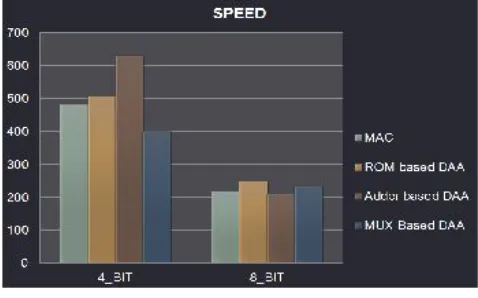
Figure 10:Speed Analysis
VI.CONCLUSION AND FUTURE WORK
Thus from the above analysis it is clear that, as compared with Multiplier based approach, the multiplexer based DAA has better performance. The MUX based DA achieved good performance in area, power compared. When both the inputs are variables and the proposed architecture performs point, line and edge detection through hardware approach. The MUX based DA has been widely adopted in many digital signals processing application such as DCT, DFT, FIR and DHT.
Our future work is to implement Point detection, Line detection, Edge detection in Digital Image processing using MUX based DAA in order to achieve better performance.
REFERENCES
[1] Raveenakoppula, S.kMasthan ,“An Efficient Distributed Arithmetic Architecture for High Order Digital Filters”, International Journal of Computer Trends and Technology, volume 2, Issue 2, 2011.
[2] Pai, A.K., Benkrid, K., Crookes, D., "Embedded reconfigurable DCT architecturesusing adder-based distributed arithmetic", CAMP, pp. 81-86, 2005.
[3] Jiun-In Guo, Rei-Chin Ju,Jia-Wei Chen,"An efficient 2-D DCT/IDCT coredesign using cyclic convolution and adder-based realization", Circuits and Systemsfor Video Technology, Volume 14, Issue 4, pp.416 – 428, 2004.
[4] Marcos R. BoschettiAlexando, "Techniques and Mechanisms forDynamic Reconfiguration in an Image Processor", Integrated Circuits and SystemsDesign, pp.177-182, 2002.
[5] Jiun-In Guo, "A new DA-based array for one dimensional discrete Hartley transform", ISCAS, vol. 4, pp.662 – 665, 2001.
[6] S. F. Haiso, W. R. Shiue, and J. M. Tseng, "Design and implementation off a novel linear-array DCT/IDCT processor with complexity of order log2N", IEE Proc.Visions, Images, and Signal Processing, vol. 147, no.5, pp. 400-408, Oct 2000.
[7] T.-S.Chang,C.Chen and C.-W. Jen, “New distributed algorithm and its application to IDCT" ,IEE Proc. –Circuits Devices Syst., Vol.146, No.4, August 1999.
BIOGRAPHY
D.Srimathi was born in Tamilnadu on 1991. She is a M.E. student of Applied Electronics department in IFET College of Engineering, Villupuram, India. She completed her Bachelor of degree in Electronics and Communication Engineering in Oxford Engineering College, Trichy, India in the year 2013.
P.Santhini was born in Tamilnadu on 1991. She is a M.E. student of Applied Electronics department in IFET College of Engineering, Villupuram, India. She completed her Bachelor of degree in Electronics and Instrumentation Engineering in Anand Institute of Higher Technology, Chennai, India in the year 2013.
M.Malarvizhi was born in Tamilnadu on 1991. She is a M.E. student of Applied Electronics department in IFET College of Engineering, Villupuram, India. She completed her Bachelor of degree in Electronics and Communication Engineering in Anand Institute of Higher Technology, Chennai, India in the year 2013.