A Design of Multiple Output DC-DC Flyback
Converter
Neha Mehrotra1, Hemavathi R2
PG Student [Power Electronics], Dept. of EE, UVCE, Bangalore, Karnataka, India1
Assistant Professor [Power Electronics], Dept. of EE, UVCE, Bangalore, Karnataka, India2
ABSTRACT: The Flyback converter is DC-DC converters used for supplying isolated and multiple outputs of different polarity. In the present era the regulated power supply is used for serving a variety of applications like aerospace, computers, TV (instrumentation), industry (factory automation) etc. The flyback converter not only provides isolation from input to output side, but is also used for low switching losses, fast transient response, low output voltage, high current etc. In the proposed paper flyback is used for generating a power supply with multiple outputs (3). The proposed flyback is designed for 28V to 3 outputs i.e., 5V, +15V, -15V. The flyback is operating in current control mode (CCM) and discontinuous current mode (DCM). The operating frequency of the converter is 100KHz. the converter is simulated by using software LTSPICE. It is software by which all the practical components can be implemented and same circuit can be designed for hardware as well.
KEYWORDS: Flybacked, Continuous conduction mode (CCM), Discontinuous conduction mode (DCM), MOSFET
I.INTRODUCTION
In today’s era SMPS has eliminated the use of linear power supplies. it consisted of 50-60 Hz heavy transformers for stepping up and down the input voltage as per the requirement. The use of these transformers results into high power losses and poor efficiency. On comparing with the switched mode power supply, it can operate at higher frequency ranging from few KHz to Mega Hz. It reduces the overall size of the circuit, provides better efficiency, low cost and less weight. There are many topologies available for SMPS, but the correct design depends upon the application.
The converters available can be AC-DC or DC-DC. In AC-DC, the AC from the mains is converted to DC with a bridge rectifier and a input capacitor. Among all the converter topologies flyback is the most easiest and popular topology. In many industrial applications, it is being implemented for obtaining a number of outputs.
Flyback converters are known for low switching losses, fast transient response, low output voltage, high current handling capability etc. The cost and size of the flyback is small. Since the converter can be operated at high frequency so the size of the magnetic components also reduces. It provides isolation between input to output side with the help of a transformer. In flyback transformer is not used practically, rather a coupled inductor. But for clarification transformer terminology is used. The transformer is referred as a coupled inductor as its primary stores energy in the steady state and transfers it to the secondary at the end of steady state.
These converters can be operated in CCM or DCM. In industries DCM mode is the most preferred. In CCM the energy stored in the transformer is not completely transferred to the secondary compared to DCM. In DCM all the stored energy is flybacked to the secondary and the secondary energy decays to zero before every switching cycle.
Multiple numbers of outputs can be obtained by increasing the count of secondary windings. By proper design, multiple outputs with different polarities can be achieved with one converter.
In the proposed paper a DC-DC flyback converter is designed with multiple outputs. The specification of the converter is 28V to 3 outputs i.e., 5V, +15V, -15V. The operating frequency of the converter is 100KHz. The converter is designed for DCM mode with the operation in current control mode. The simulation is implemented by using LTSPICE software. This software is helpful in simulating the circuit with practical components, which can be used in hardware implementation as well.
II.PROPOSED TOPOLOGY
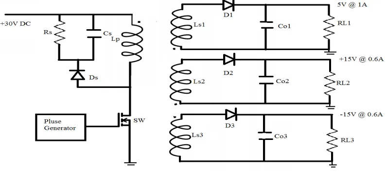
The proposed flyback converter topology is shown in figure1.1. When the switch is closed, the dotted end becomes positive with respect to the non dotted end. The primary inductor stores the energy and the forward voltage across it is Vin/Lp. During this stage no current flows in the secondary as the diode becomes reversed biased. The load current is served by the output capacitors. This is the reason the output capacitors should be large enough to drive the load with minimum droop voltage.
Figure. 1 The proposed Flyback Converter in open loop.
When the switch is open, at the end of steady stage the dotted end attains negative polarity with respect to the non dotted end. So, the secondary side diodes become forward biased and all the stored energy in the primary is flyback-ed to the secondary. The MOSFET used is given gate pulses with the help of a function generator. The function generator is set at 100 KHz switching frequency.
III.CLOSED LOOP SIMULATION
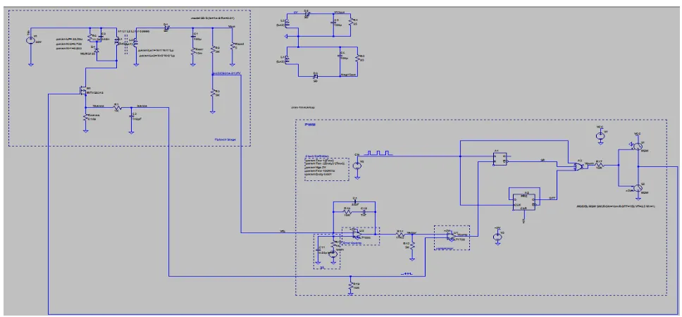
The closed is implemented using software LTSPICE. In this software practical components can be used for simulating circuit. The closed loop is tested by using error amplifier, comparator, f/f and latch. The simulation circuit for closed loop flyback converter is shown in figure 2. The first stage is the flyback stage, and the second is the PWM stage.
Figure. 2 The closed loop simulation circuit.
In the PWM stage, the output voltage 5V is taken as feedback. The 5V is first reduced to 2.5V with a resistor divider circuit. This voltage is given to the error amplifier with a reference of 2.5V. Whenever the voltage is higher than the reference, error will be generated and compared with the primary current in the comparator. This primary current is sensed with the sensing resistor. The voltage generated by the comparator is given as input to the SR latch. The output of the latch turns ON and OFF the 2 switches. The output of the switch is given as the gating pulses to the MOSFET.
The first loop is the voltage loop in which error amplifier is employed. The second loop is the current loop in which comparator is employed.
IV.SIMULATION RESULTS
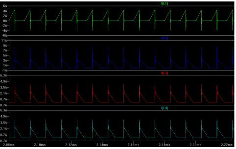
The closed simulation results are shown in the following waveform. The output voltage shown in figure 3. The middle waveform shows the 5V output which is taken as feedback, and is completely cross regulated. The above and bottom waveform shows the +15V and -15V output voltage which are semi regulated. In the flyback converter the semi regulated output have a variation of +/-10%.
Figure. 4 Primary and 3 secondaries inductor current.
When the energy stored in the primary inductor during the steady state is transferred to the secondary and the secondary current decays to zero completely before the next switching cycle, and also after the secondary current decaying to zero there is a dead time present before next switching cycle then it can be said as the flyback converter is operating in DCM mode. The figure 6 shows the converter working in DCM mode.
V. RESULT AND DISCUSSION
The proposed flyback converter is a multiple output topology, operating at 100KHz switching frequency. The circuit diagram of the proposed converter is shown, the working is explained in the above section. The closed loop simulation circuit is shown. The various waveform of the converter shows that the output which is taken as feedback is perfectly cross regulated. The other outputs are semi regulated and have +/-10% variation in output. The waveform for the current in the winding shows that the proposed topology operates in the DCM mode.
VI.CONCLUSION
The flyback converter is the most efficient topology. It is used for low power application. It has the advantage of low output voltage, isolated and multiple numbers of outputs, fast switching. The number of outputs can be easily increased by changing the count of the secondary winding. The flyback converters are used in aerospace application, process control, digital system, industry automation etc.
REFERENCES
[1] Christrophe Basso, “Switched Mode Power Supplies”. [2] Daniel W. Hart, “Power Electronics”.
[3] Alla A. Salvia, “Design Guide for Off-line Fixed Frequency DCM Flyback Converter”, Infineon Technologies North America (IFNA) Corp., Design Note DN 2013-01 V1.0 January 2013.
[4] N. Vazquez, H. Lopez, C. Hernandez, H. Calleja, “Multiple-Output DC-to-DC based on the Flyback Converter”, IEEE 2008..
[5] Nagesha C, A. Sreedevi, Muniraj Gopal, “Simulation and Hardware Implementation of 24Watt Multiple Output Flyback Converter”, IEEE International Conference on Power and Advanced Control Engineering 2015, pg 366-370, 2015.
[6] Umesh Goyal, Dr. Neelam Rup Prakash, “Design of Low Power Multiple Output Power Supply for Embedded Systems”, IEEE 4th ICCCNT
2013 July 4-6, 2013, Triuchengode, India.
[7] K.V.S. Mourya Chandra, Ravishankar Deekshit, Nageshwar Rao S, Bhoopendra Kumer Singh, “Design and Implementation of Current Mode Controlled Multiple Output Flyback Converter for Military Applications”, IEEE CONECCT 2015.
[8] C. Mullett, F. Cathell, “Improving the Regulation of Multi-Output Flyback Converters”, IEEE, pg 1923-1926, 2009.
[9] Tom Hack, Flyback Controller Improves Cross Regulation for Multiple Output Application-Design Note 344”, Linear Technology. [10] Multi-Output Flyback Off-Line Power Supply, ON Semiconductor, pg 1-23.
[11] Srivatsa Raghunath, “Isolated Multiple Output Flyback Converter Design Using TL431”, Texas Instruments, Application Report SLVA666-April 2014, pg 1-24.