Use of memories and programmable logic arrays for
asynchronous CAM
Sudha Varalakshmi
Jntu College Of Engineering,Pulivendula
ABSTRACT: in this paper a new algorithm is proposed in low power content addressable memory (CAM), which provides association between input tag and corresponding address of output data. The proposed architecture mainly depends on the sparse clustered network which is obtained from binary connections. This binary connections will eliminates most of the parallel comparison performed during a search. So, when we compare with conventional low power CAM design, the dynamic energy consumption of proposed design is significantly low. When an input tag is given to the proposed architecture computes a few possibilities for the location of matched tag and it performs the comparison on them to locate a single valid match. Now, for the purpose of simulation, CMOS technology is used. In this we discussed mainly about the design methodology which depends mainly upon the silicon area and power budgets and performance requirements.
KEY WORDS: Associative memory, content addressable memory (CAM), low-power computing, recurrent neural networks, sparse clustered networks (SCNs).
I.INTRODUCTION
To control the digital circuits and systems asynchronous reaction is necessary. This asynchronous reaction produces either mechanical or electrical solutions. Coming to synchronous reaction, it does not meet the constraints of problem and it process the solution in very slow way. But by using the synchronous reaction in modern integrated circuits, it occupies low power & space and as well as it will have good reliability. Now our main intent is to develop same features in asynchronous sequential circuits (ascs) with direct feedback. This asynchronous sequential circuits are built in conventional way by using gates, flip flops, complex modules and their designs.
By avoiding the problems of construction of hazard free nets and state assign free of crucial race then we Can get an excellent way of result in asynchronous sequential circuits.
In this mainly we are going to discuss
about the heuristic approach of
asynchronous sequential circuits. This approach consists of following properties like programmable logic array and random access memory. Coming to RAM, the
design methodology is completely
independent of memory type and coming to PLA, it applies equally to mask programmable and field programmable types. When we compared the both PLA and FPLA, FPLA is most widely used because the control applications are of two
low a volume to satisfy mask
programming. Now the main intent is to construct an asynchronous sequential circuit with few elements and to reduce the amount of design effort and to meet some of the limitations of lsi modules that is pin count. The constructed design should be directed by using computer aided design tools. In this mainly we are going to study about the properties of FPLA and RAM. Basically, content addressable memory is a type of memory which is accessed depend upon its contents. Now to access an entry in memory, a search data word is compared against the stored entries in parallel to find the match. For every stored entry a tag is associated which is used in comparison process. If once a search data word is given to input of CAM then the matching data word is retrieved within a single clock. This type of process gives a frequent and fast look up operations like translation look-aside buffers (TLBs), network routers data base accelerators,
extraction, Hough transformation, Huffman coding/ decoding, virus detection Lempel–Ziv compression, and image coding.
By using this parallel search operation in CAM, it consumes significant amount of energy. CAM architecture consists of high capacitive search line. By using circuit level techniques and architecture level techniques in CAM, the energy saving opportunities are discovered. Coming to dynamic CMOS circuit techniques, it produces low power and low cost. This circuit produces low noise margins and charge sharing. Now a sparse clustered network is introduced and implemented on FPGAs. This FPGA memory saves the short messages with lower level of computational complexity. Here the term CAM is nothing but a binary CAM which consists of preliminary results of architecture with particular parameters. In this paper a proposed system is introduced to elaborate the effect of designs degree of freedom. This proposed architecture consists of SCN- based amplifier which is coupled to CAM array. This CAM array is divided into several equally sized sub blocks which activates independently. Once the sub block is activated then the tag is compared with few entries and lowers the dynamic energy dissipation.
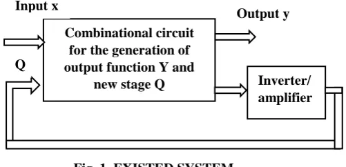
II.EXISTED SYSTEM
Below figure (1) shows the block diagram of existed system. There are some steps that should be followed in this existed system. The steps are discussed below: a) At first we should convert the given
task into a formal description.
b) Next, we should reduce the number of states which are created in step-1. Because the number heavily influences the amount of hardware.
c) A unique scale is generated to map the states into a set of binary vectors.
d) Next, transforming the formal
description into a table in the format of
binary representation of row and column identifiers.
e) The transient and output functions are derived and minimised.
f) Now this can be implemented on digital circuits.
g) Hardware realization and test will be performed on digital circuits.
h) At last the entire design is documented.
Here the steps involved in c, e, f &g are more difficult for asynchronous sequential circuits compared to sequential circuits. Because there is a rapid increase in design effort and amount of hardware. The asynchronous sequential circuit is the combination of combinational circuit and feedback loops. The both are active all the time and propagates the information all around the loop whenever change occurs. Now a stable condition is assumed in asynchronous sequential circuits to set the lines at specific level and the change in asynchronous can be done when there is change in input. So this asynchronous sequential circuits operate under three modes by depending upon the inputs and outputs, the form of transition and response time. They are given as
1) Normal fundamental mode
In this mode a single input variable changes are allowed after all changes have settle down.
2) Single transition time (STT)
In this mode one unit of overall propagation delay time is allowed for state variable changes.
Combinational circuit for the generation of output function Y and
new stage Q Inverter/ amplifier Input x
Output y
Q
3) Single output change (SOC)
Here each state transition is related to two different output vectors.
Now the main issue in this realization and application of feedback is that the generation of delay configurations under all applicable conditions. To overcome this a new system is proposed which is discussed in below section.
III. PROPOSED SYSTEM
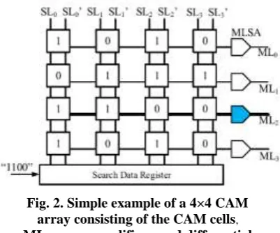
In this let us first discuss about the CAM array. The below figure (2) shows the example of 4×4 CAM array consists of
CAM cells, sense amplifiers and
differential SLs. A search data register is used to store the input bits. The register applies the search data on the differential SLs, which are shared among the entries. Then, the search data are compared againstall of the CAM entries. Each CAM-word is attached to a common match line (ML) from its constituent bits. Since the MLs are highly capacitive, a sense amplifier is typically considered for each ML to increase the performance of the search operation.
The below figure (3) shows the
architecture of proposed system. As we discussed earlier that in this we use SCAN
based amplifier. The SCAN based
classifier consists of mainly two parts they are, 1) PI and 2) PII. In PI, the neuron is binary and it is correspond to input tags and grouped to c equally sized clusters with l neurons. Generally, in two situations
the input tag is processed in SCN based classifier that is training and decoding. By using this training or decoding processes, the input tag is reduced in length to q bits, and then divided into c equally sized partitions of length κ bits.
Now the each partition is mapped to the index of neuron corresponding to the cluster of P1. The index of neuron is activated by using binary to integer mapping. Now if the given parameter is l, then the number of clusters are calculated as c = q/ log2 (l).From this we can observe that there are no connections between neurons. This is about part PI and coming to part PII, it is a single cluster consists of M neurons and it is equal to the number of entries in CAM. Each neuron in part PII is connected to the every neuron in PI. The binary value of this part PII is equal to either 0 or 1. The entire process in proposed system involves three steps they are given below and discussed in below section
1) Network training
2) CAM entry
3) TAG decoding
1) Network training: Here the binary
values in SCN based classifier
represents the association of input tags
and corresponding outputs.The
connection values are set during the training process, and are stored in a memory module. When the connection value is set to 1 then there exists an association between the corresponding neuron in PI and a CAM entry which is represented as a neuron in PII.
Fig. 3. PROPOSED SYSTEM
Fig. 2. Simple example of a 4×4 CAM array consisting of the CAM cells,
2) Network update: In SCN-CAM a network update is needed to retrain the entire SCN classifier with possible entries. The main reason to update the network is that the output neurons of PII are independent from each other and by deleting the connections from a neuron PII to the corresponding connections in PI, a tag can be deleted. Now adding new connections to the same neuron in PII adds a new entry to the SCN based classifier.
3) Tag decoding: once the SCN based classifier is trained then a tag is received and this tag determines which neuron in PII should be activated by depending upon the q bits of tag. This
process is known as decoding.
Decoding process mainly involves into four steps they are
1) An input tag is reduced in length to q
bits and divided into c equally sized partitions. 2) Next one is local decoding (LD), by using direct binary-to-integer mapping single neuron per cluster in PI is activated. 3) Global Decoding (GD), GD determines which neuron(s) in PII must be activated based on the results from LD and the stored connection values. 4) At last, ifmore than one neuron are activated in PII, then, the same number of word comparisons are required to detect the correct match.
IV. RESULTS
.
V. CONCLUSION
In this paper we studied about the architecture of low power CAM that is SCN CAM which employs the associate mechanism that is SCN-CAM classifier. This SCN-CAM amplifier is suitable for low power applications like frequent and parallel look up operations. By using independent nodes in the output part of SCN-CAM’s training network, simple and fast updates can be achieved. SCN-CAM eliminates most of the comparison
operations in the given uniform
distribution. Based upon the application the non-uniform inputs results in high power consumptions. But this does not affect the final result which is obtained from SCN-CAM. Conventional NAND-type and NOR-NAND-type architectures are also implemented in the same technology to compare SCN-CAM against with other recently developed CAM architectures.
VI. REFERENCES
[1] BEISTER, J.: 'A unified approach to combinational hazards', IEEE Trans. 1974, C-23, pp. 566-575
Fig. 4. RTL SCHEMATIC
Fig. 5. TECHNOLOGY SCHEMATIC
[2]BEISTER, J.: 'Ein totzeitmodell fuer asynchrone schaltwerke' Nachrichtentech. Z., 1975, 28, pp. 13-17
[3] BIRKNER, J., BLACK, B.,
FRANKLIN, P. and WASER. S.: PAL Handbook (Monolithik Memories Inc., 1978)
[4] DITZINGER, A.: 'Untersuchungen an
asynchronen RAM/PLASchaltwerken'.
Diploma Thesis, Institute forInformation Processing, University of Karlsruhe, Germany, 1977
[5 ]FLEISHER, H., and MAISSEL, L.I.: 'An introduction to array logic', IBM. Res.
& Dev., 1975, 19, pp. 98-109.
[6] A. Agarwal et al., “A 128×128 b
high-speed wide-and match-line\ content
addressable memory in 32 nm CMOS,” in
Proc. ESSCIRC, Sep. 2011, pp. 83–86.
[7] Y.-J. Chang and M.-F. Lan, “Two new techniques integrated for energyefficient TLB design,” IEEE Trans. Very Large Scale Integr. (VLSI) Syst., vol. 15, no. 1, pp. 13–23, Jan. 2007.
[8] H. Chao, “Next generation routers,”
Proc. IEEE, vol. 90, no. 9, pp. 1518–1558,
Sep. 2002.
[9] N.-F. Huang, W.-E. Chen, J.-Y. Luo, and J.-M. Chen, “Design of multifield IPv6 packet classifiers using ternary
CAMs,” in Proc. IEEE
GlobalTelecommun. Conf., vol. 3. 2001,
pp. 1877–1881.
[10] M. Meribout, T. Ogura, and M. Nakanishi, “On using the CAM concept for parametric curve extraction,” IEEE
Trans. Image Process., vol. 9, no. 12, pp.