CPW-Fed UWB Compact Antenna for Multiband Applications
Saira Joseph1, *, Binu Paul1, Shanta Mridula1, and Pezholil Mohanan2
Abstract—A planar UWB antenna with added GSM 1800/WMTS and UMTS bands is presented. A CPW-fed circular patch is used to obtain wideband characteristic covering the UWB range. A novel slot formed by merging the alternate sides of a hexagon with isosceles triangles is inserted in the patch to obtain dual-band operation with the lower band suitable for GSM 1800 operation. By inserting a bent monopole in the space created by the slot, a triple-band antenna is developed with two lower bands suitable for WMTS and UMTS operation. The antenna prototype is fabricated and tested. Simulated and experimental results are in good agreement. The antenna exhibits stable radiation characteristics and nearly constant group delay in the UWB range.
1. INTRODUCTION
With the increase in demand of wireless communication systems, personal communication devices are required to operate at multiple frequencies to cater to different applications. In addition to multiband operation, it is necessary that the antenna is small with light weight, low profile and easy integration with other circuit structures. Coplanar waveguide (CPW)-fed antennas have gained considerable attention due to their many attractive features such as wide bandwidth, simple structure with single metallic layer and easy integration with monolithic microwave integrated circuits. Several research articles have proposed multiband operation using slot antennas [1–3], monopole antennas [4–7], fractal antennas [8– 11], etc., and it is well known from literature that the lowest operation frequency of the antenna determines the overall size of the antenna. Presently, the focus has shifted to antennas that work in the ultra-wide band (UWB) range used for short range and high data rate communications. Recently, small size antennas have been designed for UWB systems to cover the interval 3.1–10.6 GHz [12–14]. However, most of the work presented so far use separate antennas for lower bands and UWB applications.
In this article, a CPW-fed circular patch is used to attain wideband response. Dual-band operation with a lower band from 1.68–2.06 GHz for Global Systems for Mobile (GSM: 1.71–1.88 GHz) and upper band from 3.27–11 GHz for Ultra Wide Band (UWB: 3.1–10.6 GHz) is obtained by inserting a slot in the patch such that the perimeter of the slot is an integer multiple of quarter wavelength of the GSM 1800 band resonant frequency. A triple-band antenna with two lower resonant bands from 1.36–1.47 GHz for Wireless Medical Telemetry Service (WMTS: 1.395–1.4 GHz) and 1.9–2.25 GHz for Universal Mobile Telecommunication Systems (UMTS: 1.92–2.17 GHz) and 3.14–10.8 GHz for UWB is also developed by inserting a bent monopole in the space created by the slot in the circular patch. The lower bands are achieved without increasing the overall dimensions of the antenna which makes the design compact. The paper is organized as follows. The design details and parametric study of the dual-band antenna are presented in Section 2 while the triple-band antenna is presented in Section 3. Comparisons of simulated and measured results are presented in Section 4 followed by the conclusion in Section 5.
Received 24 November 2014, Accepted 22 January 2015, Scheduled 30 January 2015
* Corresponding author: Saira Joseph (saira [email protected]).
2. DUAL-BAND ANTENNA DESIGN AND PARAMETRIC STUDY
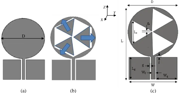
The geometry of the proposed antenna is shown in Figure 1. To develop the antenna, first a circular patch is designed with diameterD. Then a hexagonal slot is inserted in the patch and the sides of three isosceles triangles are merged with alternate sides of the hexagon as shown in Figure 1(b). The vertices of the three triangles are separated from each other by gs. The final design layout of the proposed antenna is shown in Figure 1(c).
The antenna is fed by a 50 Ω CPW on a substrate of sizeW×L. The substrate used is of thickness
h= 1.6 mm and relative dielectric constantr = 4.4 with loss tangent tanδ = 0.02. The CPW-feed line has a width Wf and is spaced at a distance ‘g’ from the ground plane of length Lg and width Wg on both sides. The circular patch of diameterD is designed [15] to cover the UWB range and is spaced at a distance ‘s’ from the ground conductor.
The slot inserted in the patch has a perimeter that is an integer multiple of a quarter wavelength evaluated as
nλg
4 =
nc
4fr√reff (1)
wherecis the free space velocity,fr is the resonant frequency andreff is the effective dielectric constant of the substrate given by the approximate formula
reff = r+ 1
2 (2)
The proposed antenna is simulated using Ansys HFSS software and optimized dimensions are shown in Table 1.
Parameters Lg, Wg, Wf, g and s affect the impedance matching in the UWB range and are optimized for wideband response in the initial circular patch [16]. To understand the dependence of the lower band on the slot parameters, parametric study is first done for the side lengthLs of the slot as shown in Figure 2, with gs = 1.2 mm and all other antenna parameters fixed at the values given in Table 1.
D
Y Z
X
(a) (b) (c)
Figure 1. (a) UWB circular patch. (b) Formation of slot shape. (c) Geometry of proposed dual-band antenna.
Table 1. Dual-band antenna dimensions (mm).
Parameter L W D Ls gs Lg Wg Wf g s
As slot length increases, the first resonance frequency as well as the lower cut off of the UWB range shifts towards the lower frequencies. For Ls = 16.7 mm, the slot perimeter is approximately 150 mm which corresponds to 1.5λg of the resonance frequency in the GSM 1800 band and so this dimension is chosen for slot side length. Next the slot gapgsat the centre of the slot is varied. TheS11vs frequency curve is shown in Figure 3. As slot gap is increased, better matching is achieved in the UWB range but the first resonance and lower frequency limit of the UWB band increases slightly. This could be due to the decrease in the overall slot perimeter with increase in slot gap. Optimum results are obtained forgs= 1 mm. The orientation of the slot with respect to the feed line is also an important parameter in determining the impedance bandwidth of the antenna. To study its effect, the slot is rotated 30◦ clockwise and counterclockwise and the results are shown in Figure 4.
When the slot is placed symmetrically with respect to feed line as shown in the second orientation there is significant shifting in the lower frequency limit of the UWB band. In the third orientation, there is considerable mismatch in the UWB range. The first resonance however remains unchanged for all three orientations because slot dimensions are the same in all three cases. The current distribution on the surface of the antenna at the first resonant frequency is shown in Figure 5. The current concentration
Figure 2. S11vs frequency of the proposed dual-band antenna for various lengths of slot side Ls withgs= 1.2 mm.
Figure 3. S11 vs frequency of proposed dual-band antenna for varying slot gap gs with Ls = 16.7 mm.
Figure 4. S11 vs frequency of the dual-band antenna for various orientations of the slot with
Ls= 16.7 mm and gs= 1 mm.
Figure 6. Simulated radiation efficiency of proposed dual-band antenna.
Ls (mm) r h (mm)
fr (GHz) Simulated
in HFSS
16.98 4.4 1.2 1.86
17.7 2.7 2.5 1.85
17.54 4 0.8 1.95
17.72 3 2 1.87
17.38 3.66 1.6 1.89
17.36 3.3 2.2 1.88
18.18 2.2 2.4 1.81
Table 2. Simulated resonance frequencies for lower band on different substrates.
along the edges of the slot clearly reveals that the perimeter of the slot controls the first resonance. The radiation efficiency of the antenna is shown in Figure 6. The efficiency is above 85% in the GSM 1800 and UWB bands and decreases sharply between 2 and 3 GHz as this is not an intended band of operation.
The proposed dual-band antenna is simulated on substrates of different dielectric constants r and thicknesses h. Using regression analysis, the required perimeter of the slot for a given resonance frequencyfr is
Perimeter≈9Ls−47.98fr−7.655r−5.02h+ 278.89 (3)
This equation is applicable to substrates with 2.2 ≤ r ≤ 4.4 and 0.8 ≤ h ≤ 2.5. To validate the equation, the antenna is simulated for a lower resonance band at 1.8 GHz on different substrates and the results obtained are shown in Table 2.
On all the substrates the proposed method can be used to attain dual-band behavior which ensures repeatability of the design.
3. TRIPLE-BAND ANTENNA DESIGN AND PARAMETRIC STUDY
In order to develop a triple-band antenna, a bent monopole is inserted in the space created by the slot. The monopole is made up of three segments of lengths LM1,LM2 andLM3 of widthLMw. The monopole will be efficiently excited if it is placed along the direction of current flow near the main CPW feed line. To accommodate the monopole in this manner, a portion of the patch is cut away near the feed and the monopole is spaced at a distance tfrom the slot edge as shown in Figure 7.
The overall length of the monopole isLM1+LM2+LM3and corresponds to a quarter wavelength of the resonance frequency 2.2 GHz suitable for UMTS application. The length of the monopole increases the overall perimeter of the slot and this lowers the first resonance frequency to 1.4 GHz which is suitable for WMTS applications. The dimensions of the optimized triple-band antenna are as given in Table 3. To carry out the parametric study of the bent monopole, first the segment length LM1 is varied, and S11 results are shown in Figure 8. As the length of the segment increases, the first two resonance frequencies shift towards the lower frequency side but matching in these bands is poor. For lower
Table 3. Dimensions of triple-band antenna (mm).
Parameter L W D Ls Lg Wg Wf g s LM1 LM2 LM3 LMw t
g L
W D
Ls
L M1
Wg s LM
t
Lg LM3
LM2
Wf Y
Z
X
w
Figure 7. Geometry of the proposed triple-band antenna.
Figure 8. S11vs frequency of the proposed triple-band antenna for varyingLM1 withLMw=1 mm and t= 0.6 mm.
(a) (b)
Figure 9. Surface current distribution of the proposed triple-band antenna at (a) 1.4 GHz, (b) 2.2 GHz.
Figure 10. Simulated radiation efficiency of proposed triple-band antenna.
segment lengths the matching at upper frequencies degrades. With LM1 = 10 mm there is reasonably good impedance matching in all the intended bands of operation.
The surface current distribution at the two resonant frequencies is shown in Figure 9. It is seen that at 1.4 GHz the current is distributed on the monopole as well as on the perimeter of the slot. At 2.2 GHz quarter wavelength distribution is seen along the length of the monopole element.
Figure 11. S11 vs frequency of triple-band antenna for varyingLMwwithLM1 = 10 mm and
t= 0.6 mm.
Figure 12. S11 vs frequency of triple-band antenna for varying t with LM1=10 mm and LMw= 1 mm.
(a) (b)
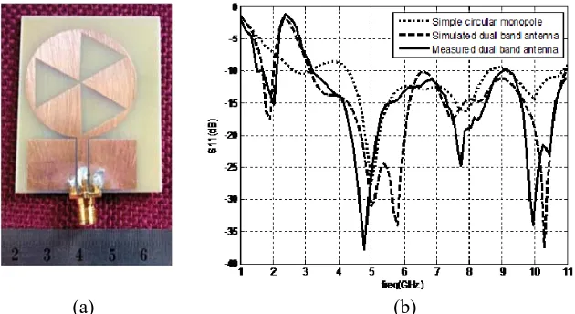
Figure 13. (a) Fabricated dual-band antenna. (b) Measured and simulated S11 vs frequency.
4. EXPERIMENTAL RESULTS
Using the optimized dimensions listed in Tables 1 and 3, prototypes of the dual-band and triple-band antennas are fabricated as shown in Figure 13(a) and Figure 14(a) respectively. Experimental verification is carried out on HP8510C network analyzer. The measured and simulated results are compared in Figure 13(b) and Figure 14(b).
The simulated and measured readings are found to be in good agreement for both antennas at lower frequencies. At higher frequencies, there is mismatch, but this can be attributed to soldering effects that have not been accounted for in simulation studies. The operating bands for S11 < −10 dB are 1.68–2.06 GHz and 3.27–11 GHz in the dual-band antenna and 1.36–1.47 GHz, 1.9–2.25 GHz and 3.14– 10.8 GHz in the triple-band antenna. The normalized radiation patterns measured at various radiated frequencies are shown in Figure 15 and Figure 16.
The patterns have a near Figure 8 shape in theE-plane and are non directional in theH-plane. A slight rotation is seen in theE-plane patterns of both antennas which can be attributed to measurement errors. Also, at higher frequencies the shape is somewhat distorted which is due to the excitation of higher modes as commonly seen in such antennas.
(a) (b)
Figure 14. (a) Fabricated triple-band antenna. (b) Measured and simulatedS11 vs frequency.
(a) (b)
1.8 GHz
3.3 GHz
6 GHz
10 GHz
Figure 15. Normalized radiation pattern of dual-band antenna measured in (a)E-plane (Y-Z plane), (b)H-plane (X-Y plane).
1.4 GHz
2.2 GHz
6 GHz
10 GHz
(a) (b)
Figure 17. Measured group delay of dual and triple-band antenna.
Figure 18. Measured peak gain of dual and triple-band antenna.
measured readings are shown in Figure 17.
The readings are almost constant with a slight variation between 7.5 and 8 GHz. The group delay is higher in this range for the triple-band antenna which is due to the introduction of the bent monopole at the feed point which makes the lower part of the patch have a more meandered current path. The antenna is thus suitable for multi-band orthogonal frequency division multiplexing (MB-OFDM) UWB systems in which the UWB range is divided into 14 subintervals each with a bandwidth of 528 MHz [22]. In the rest of the UWB range the group delay variation is less than 1 ns.
The measured gain [18] of the two antennas is shown in Figure 18. For the dual-band antenna the gain is 2.82 dBi at 1.8 GHz while in the UWB range the maximum gain is 7.35 dBi. For the triple-band antenna the gain is 6.9 dBi at 1.4 GHz, 0.2 dBi at 2.2 GHz and a maximum gain of 8.17 dBi in the UWB range. When compared to a simple CPW-fed circular monopole [16] of diameter 30 mm where the first resonance frequency occurs at 2.57 GHz, the lowest frequency of operation of the dual/triple-band antenna is considerably reduced by the proposed method for similar patch diameter. The overall size of the proposed antenna is larger than that of [19] but has the advantage of CPW-feed. The antenna size in [20] is also smaller than this design, but its lowest frequency of operation is higher. In [21], the lowest operation band is at 800 MHz but the structure is not planar and is designed specifically for smartphones.
5. CONCLUSION
CPW-fed dual- and triple-band antennas for UWB operation with added lower bands suitable for GSM 1800/WMTS and UMTS operation are proposed. While a conventional circular monopole is used to attain UWB response, the introduction of a novel slot results in a lower band of operation whose resonant frequency depends on the perimeter of the slot. By introducing a bent monopole in the space created by the slot, two lower bands are achieved for triple-band operation. In both the antennas lower frequency of operation is attained without increasing the overall size of the UWB antenna. The antennas have nearly omnidirectional radiation patterns and constant group delay in the UWB range. The radiation characteristics and the compact size make the proposed antennas suitable for multiband wireless communication devices.
ACKNOWLEDGMENT
REFERENCES
1. Chen, S. W., D. Y. Wang, and W. H. Tu, “Dual-band/tri-band/broadband CPW-fed stepped impedance slot dipole antennas,”IEEE Transactions on Antennas and Propagation, Vol. 62, No. 1, 485–490, Jan. 2014.
2. Zhang, S. M., F. S. Zhang, W. M. Li, W. Z. Li, and H. Y. Wu, “A multiband monopole antenna with two different slots for WLAN and WIMAX applications,” Progress In Electromagnetics Research Letters, Vol. 28, 173–181, 2012.
3. Chiang, M. J., S. Wang, and C. C. Hsu, “Compact multifrequency slot antenna design incorporating embedded arc-strip,”IEEE Antennas and Wireless Propagation Letters, Vol. 11, 834–837, 2012. 4. Yao, Y., X. Wang, and J. Yu, “Multiband planar monopole antenna for LTE MIMO systems,”
International Journal of Antennas and Propagation, Vol. 2012, Article ID 890705, 2012.
5. Lee, C. H., Y. H. Chang, and C. E. Chiou, “Design of multi-band CPW-fed antenna for triple-frequency operation,”Electronics Letters, Vol. 48, No. 10, 543–545, May 2012.
6. Mirkamali, A., L. Akhoondzadeh-Asl, P. S. Hall, and K. Moussakhani, “Modified multiband multiple ring monopole antenna,”Progress In Electromagnetics Research C, Vol. 14, 173–183, 2010. 7. Hongnara, T., C. Mahattanajatuphat, P. Akkaraekthalin, and M. Krairisksh, “A multiband CPW-fed slot antenna with fractal stub and parasitic line,” Radioengineering, Vol. 21, No. 2, 597–605, Jun. 2012.
8. Khan, O. M., Z. U. Islam, I. Rashid, F. A. Bhatti, and Q. U. Islam, “Novel miniaturized Koch pentagonal fractal antenna for multiband wireless applications,”Progress In Electromagnetic Research, Vol. 141, 693–710, 2013.
9. Viani, F., “Dual-band Sierpinski pre-fractal antenna for 2.4 GHz-WLAN and 800 MHz-LTE wireless devices,” Progress In Electromagnetics Research C, Vol. 35, 63–71, 2013.
10. De Dieu, N. J. and W. Zhou, “Koch-based circular CPW fed dual UWB antenna,” 2013 IEEE Conference on Microwave Technology and Computational Electromagnetics (ICMTCE), 200–203, Aug. 2013.
11. Aziz, R. S., M. A. S. Alkanhal, and A. F. A. Sheta, “Multiband fractal-like antennas,”Progress In Electromagnetics Research B, Vol. 29, 339–354, 2011.
12. Nazli, H., E. Bı¸cak, B. T¨uretken, and M. Sezgin, “An improved design of planar elliptical dipole antenna for UWB applications,”IEEE Antennas and Wireless Propagation Letters, Vol. 9, 264–267, 2010.
13. Bataller, M. F., M. C. Fabr´es, E. A. Daviu, and A. V. Nogueira, “Overview of planar monopole antennas for UWB applications,” Proceedings of European Conference on Antennas and Propagation 2006, Nice, France, Nov. 6–10, 2006.
14. Lin, C. C. and H. R. Chuang, “A 3–12 GHz UWB planar triangular monopole antenna with ridged ground-plane,”Progress In Electromagnetics Research, Vol. 83, 307–321, 2008.
15. Garg, R., P. Bhartia, I. Bahl, and A. Ittipibon, Microstrip Antenna Design Handbook, Artech House, Boston, London, 2001.
16. Liang, J., L. Guo, C. C. Chiau, and X. Chen, “CPW-fed circular disc monopole for UWB applications,” Antenna Technology: Small Antennas and Novel Metamaterials, IWAT 2005, 505– 508, 2005.
17. Bazaz, R., S. K. Koul, M. Kumar, and A. Basu, “An ultra wideband antenna with band rejection capability and its characterization in time domain,” Progress In Electromagnetics Research C, Vol. 19, 223–234, 2011.
18. Balanis, C. A.,Antenna Theory: Analysis and Design,John Wiley and Sons, New York, 1997. 19. Foudazi, A., H. R. Hassani, and S. M. Ali Nezhad, “Small UWB planar monopole antenna with
added GPS/GSM/WLAN bands,” IEEE Transactions on Antennas And Propagation, Vol. 60, No. 6, 2987–2992, Jun. 2012.
21. Akiyama, Y., F. Koshiji, and K. Koshiji, “A multiband antenna with fan-shaped monopole and folded element of 800 MHz, 2.0 GHz and UWB for 4G smartphones,” International Conference on Electronic Packaging 2014 Proceedings, 494–497, 2014.