Induction Motor Speed Control Using Space
Vector Pulse Width Modulation
P.Raju1, S.Nagaraju2, T.Jaganmohan Rao3
P.G. Student, Department of EEE, AITAM Engineering College (Autonomous), Andhra Pradesh, India1
Associate Professor, Department of EEE, AITAM Engineering College (Autonomous), Andhra Pradesh, India2
Asst. Professor, Department of EEE, AITAM Engineering College (Autonomous), Andhra Pradesh, India3
ABSTRACT: This paper presents generalized space vector pulse width modulation (SVPWM) scheme for multilevel inverter. The SVPWM scheme generates all the available switching states and switching sequences based on two simple and general mappings, thus independent of the level number of the inverter. The generalized method of generating the switching states (first mapping), calculating duty cycles, and determining the switching sequence (second mapping) is described in this paper. The scheme is suitable for every reference vector with any modulation index, and can be conveniently extended to meet specific requirements, such as symmetric switching sequences. Comparing with previous methods, the SVPWM scheme proposed in this paper provides two more degrees of freedom, i.e., the adjustable switching sequences and duty cycles, thus offering significant flexibility for optimizing the performance of multilevel inverters. In this paper, open loop speed control of three phase induction motor using space vector pulse width modulation is presented by using MATLAB/SIMULINK model.
KEYWORDS: SVPWM, 3φ-Induction motor, adjustable duty cycles, redundant switching states
I. INTRODUCTION
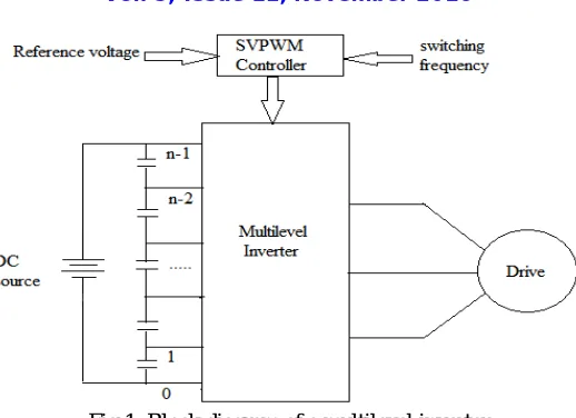
Fig 1: Block diagram of a multilevel inverter
A Euclidean vector system based SVPWM algorithm is presented in [1]. However, several matrix transformations are needed, and do not provide either systematic approach for determining the switching sequences or real time implementation. A coordinate transformation and switching sequence mapping based SVPWM scheme is proposed in [2], in which a coordinate transformation is needed to determine the location of the reference vector and to calculate the duty cycles, and a pre stored switching sequence mapping table is needed to determine the switching sequence. The three level space vector diagram can be partitioned into six two level space vector diagrams [9]. However, for the calculation of on – time, the origin is shifted to one of the six centres and the axes are rotated by 60˚.
This new SVPWM scheme has the following salient features:
1. Switching states, duty cycles and switching sequences are all obtained by simple calculation; less memory is needed and it is computationally fast.
2. The SVPWM scheme proposed in this provides two more degrees of freedom i.e. adjustable switching states and switching sequences.
3. The scheme works good for any reference vector with any modulation index.
II. BASIC PRINCIPLE OF THE SVPWM SCHEME
For an N level inverter shown in Fig 1: the output voltage vector is defined as
V = V (S + S e / + S e /
) (1)
Where Vdc is voltage of the dc source, and Sa, Sb, and Sc are the switching states of Phase A, B and C respectively. If the
values of Sa, Sb, and Sc are defined as Sa , Sb, Sc = 0,1, 2...N-1, then the output voltages of phases A, B and C relative
to the negative terminal of the dc source are Sa . Vdc/(n-1), Sb . Vdc/(n-1), Sc .Vdc/(n-1), respectively. The definition in
equation (1) is still suitable, when the N – level inverter is a cascaded inverter and in this condition Vdc/(n-1) represents
the smallest voltage among the separate dc sources.
Based on equation (1) a space vector diagram contains all the output vectors and the corresponding switching states of the inverter can be generated. For example Fig 2 shows the space vector diagram of a 7 level inverter calculated in this way. In the space vector diagram, the number at each vertex represents the switching state SaSbSc of the inverter, where
Sa, Sb and Sc are respectively the switching states of phases A, B and C as in (1). For example, the number 061 at vertex
P1 means that for the vector OP1, the corresponding switching states of phases A, B and C are Sa = 0, Sb = 6, and Sc = 1.
for generating the vector with tip P4, and they are listed decreasingly from top to bottom corresponding to the switching
states of phase A.
A reference vector Vref and the corresponding “nearest three vectors” OP1, OP2, and OP3 are also shown in Fig 2. The
vertices of the nearest three vectors to create called as “modulation triangle”, which encloses the reference vector. In order to synthesize or equate the reference vector, it is the task of the SVPWM scheme to detect the nearest three vectors (i.e., the switching states of the vertices P1, P2, and P3), to determine the sequence of the nearest three vectors
during a switching cycle (i.e., the switching sequence), and to calculate the needed on- time (i.e., duty cycle) of each nearest vector based on the following equation.
Ts .Vref = d1 . OP1 + d2 .OP2 + d3 .OP3 (2)
Where Ts is the command switching cycle, and d1, d2, and d3 are the duty cycle periods of OP1, OP2, and OP3 respectively.
Fig 2: Space vector diagram of seven level inverter
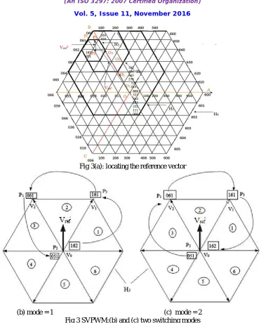
The SVPWM scheme proposed in this paper is illustrated in Fig 3. Fig3(a): shows how to locate the reference vector
(i.e., to detect the modulation triangle ΔP1P2P3); Fig. 3(b) and (c) shows how to locate the duty cycles and to generate
the switching sequence in two modes, i.e., counter clockwise (mode =1) and clockwise (mode =2 ), as if it were an equivalent two level SVPWM. In Fig. 3(b) and (c), V0, V1, and V2 are, respectively, equivalent to the nearest three
vectors OP2, OP3, and OP1. Fig 3 is described in more detail. The proposed SVPWM illustrated is based on the space –
vector diagram of a seven level inverter is shown in Fig 2.
III. LOCATING THE REFERENCE VECTOR
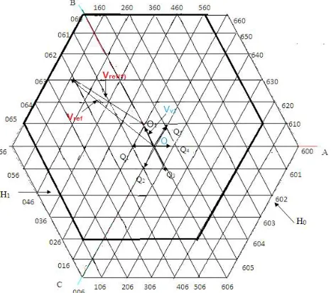
First, the reference vector Vref is represented as the sum of a set of “vertex vectors” (OO1, O1O2, O2O3, O3O4 and O4P2)
and a “remainder vector” Vref’, as shown in Fig 3(a). A vertex vector is a vector containing two adjacent vertices. The
vertex vectors connect the centre vertex of the N - level space vector diagram H0 with a first vertex (P2) of the
modulation triangle (ΔP1P2P3) enclosing the reference vector. The reminder vector is enclosed by the modulation
triangle and connecting the first vertex of the modulation triangle with the reference vector.
One way to determine the set of vertex vectors is based on determining a set of nested hexagons H1, H2, and H3
Fig 3(a): locating the reference vector
(b) mode = 1 (c) mode = 2 Fig 3 SVPWM:(b) and (c) two switching modes
Each nested hexagon corresponds to a specific level ranging from (N -1) to a second level, and centres at the vertex of a vertex vector. For instance, the method of selecting the nested (N -1) level hexagon H1 is shown in Fig 4. In this way
the other nested hexagons can be selected.
As shown in Fig 4(a), the N- level space – vector diagram H0 is partitioned into six sectors by six dashed lines. The six
dashed lines pass through the centre of the N- level space – vector diagram and their angles are from π/6 to 11π/6, and the angle between any two adjacent dashed lines is π/3. Consider the N- level space vector diagram as being composed of six hexagons that are the space – vector diagrams of (N-1) level inverters, and whose centre vertices (O1, and Q1 –
Q5) compose a two level hexagon enclosing the centre of H0. For clarity, only three hexagons SH1, SH2, and SH3 of the
Fig 4(a): division of the space vector diagram
Consequently, the nested (N-1) level hexagon H1 is selected as the one whose centre locates in the same vector as the
reference vector does (i.e., SH3), which in Fig 4(a) means that the angle θ0 of the reference vector has values within the
following range:
π/2 ≤θ0≤5π/6 (3)
The first vertex vector Vv1 is the vector that connects the centre vertices of H0 and H1, as shown in Fig 4(a).Another
equivalent way to determine the vertex vector is shown in Fig 4(b). There are six vectors available for the nested (N-1) level hexagon H1, which indicates black solid arrows (OO1) and (OQ1 – OQ5)are shown in Fig 4(b). The actual vertex
vector, among the six available vertex vectors, for the nested (N-1) level hexagon H1, is the one for which the angle
between this vertex vector and the reference vector is the smallest. In this way, the first vertex vector Vv1 can also be
selected, as shown in Fig 4(b).
Generally, the angle (φ1) of the first vertex vector are determined by the angle θ0(0 ≤ θ0 ˂ 2π) of the reference vector as
φ1 = int{mod(θ0+π/6, 2π). 3/π}.π/3 (4)
Where the function int(x) means the integer part of x, and the function mod(x, y) represents the remainder of x divided by y. After the first vector is determined, the origin of the reference vector Vref is shifted to the centre vertex of H1,
which yields a new reference vector Vref(1) as
Vref(1) = Vref – Vdc.℮jφ1 (5)
Based on Vref(1), all the other nested hexagons and vertex vectors can be determined by repeating the process shown in
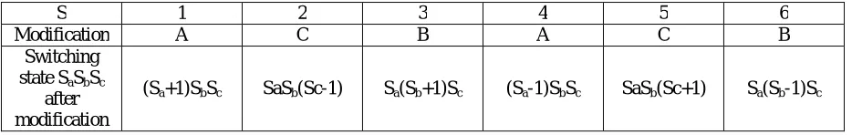
Fig 4 and the calculation by using equations (4) and (5).After the set of vertex vectors is obtained, determine iteratively the switching states at the vertices (i.e., centres of the nested hexagons) for each vertex vector in the set of vertex vectors, starting from the present switching states of the inverter at the origin vertex, by modifying (increase or decrease by 1) a corresponding phase of the present switching states to produce the switching states of the inverter at the first vertex (P2 in Fig 3) of the modulation triangle. The type of the modification for the switching states and the
corresponding phases are shown in Table I, which is called the “first mapping” in this paper and will be explained later. For each iteration, the type of the modification and the corresponding phase are determined based on a function s [represents the order number of the sector containing the reference vector as in Fig 4(a)] of the angle φ of the corresponding vertex vector relative to axis A, and the function s of the angle φ (0 ≤ φ ˂ 2π) of the corresponding
vertex vector can be described as
S = 3φ/π + 1 (6)
The rule of the modification for the switching states (first mapping) according to the function s is shown in Table I, in which the letters A, B, or C mean the switching state of phase A, B or C respectively, that needs to be modified. The up arrow “↑” means that the switching state of the phase needs to increased by 1, and the down arrow “↓” means that the
switching state of the phase needs to decreased by 1. For example, if a switching state is SaSbSc and the modification
rule is “A↑” (S =1), then the switching state after the modification is (Sa+1)SbSc.. The switching states after the
modification for other values of S are also abridged in Table I
Table I: Rule of the modification of Switching States (First Mapping)
S 1 2 3 4 5 6
Modification A C B A C B
Switching state SaSbSc
after modification
(Sa+1)SbSc SaSb(Sc-1) Sa(Sb+1)Sc (Sa-1)SbSc SaSb(Sc+1) Sa(Sb-1)Sc
Since the switching state for each phase of an N – level inverter can only have a value from 0 to (N-1) by definition in this paper, a switching state needs to be excluded when the corresponding switching state of phase A, B or C is larger than (N-1) or less than 0.
Fig 5: Switching states at the first vertex of the modulation triangle and the vertex vectors
For example, for the vertex vector from the centre of H2 to the centre of H3, the value of S in equation (6) is S3 = 4; thus,
the modification rule according to Table I is “A↓”. Because the switching states at the centre of hexagon H2 are 262,
151, and 020, the switching states at the centre of hexagon H3 (the first vertex P2 of the modulation triangle) can be
calculated as 162 and 051(the invalid switching state -120 is removed)
The rationale for the first mapping (see Table I) is based on equation (1). For a vertex vector, the shift of the origin of the reference vector is Vdc. ℮j(s – 1)π/3 (S is calculated in equation (6)), which can be substituted into equation (1) to
determine the required modification for the present switching states of phase A, B or C. The first mapping is suitable for any level inverter and any reference vectors with any modulation indexes.
IV. CALCULATING DUTY CYCLES
Based on the remainder vector Vref1, as shown in Fig. 3(b) and (c), the duty cycles of the “nearest three vectors” are
determined as for a two – level SVPWM, thus independent of the level number of the inverter. V0, V1, and V2 are
respectively, equivalent to the nearest three vectors OP2, OP3, and OP1. Equation (2) is now expressed as
Ts .Vref1 = Vdc . (T1 . ℮j(reg-1)π/3 + T2 . ℮jreg.π/3 ) (7)
Where Ts is the commanded switching cycle; T1 and T2 are, respectively, the duty cycle periods of V1 and V2 ; reg is the
region number (1 – 6) of the modulation triangle in the nested two – level hexagon H3 as shown in Fig 3(b) and (c), and
can be calculated as
reg = int(3θrem/π) + 1 (8)
Where θrem (0≤θrem˂2π) is the angle of the reminder vector, and int(3θrem/π) means the integer part of 3θrem/π. For
example, reg = 2 in Fig. 3 (b) and 3(c). .
Finally the duty cycles are T =
√ V sin π −V cos . T (9)
T = √ V sin π −V cos . T (10)
T0 = TS – T1 – T2 (11)
Where Vrx and Vry represents the real and imaginary part of Vref’/Vdc, respectively; T0 is the total duty cycle period for
the vectors from the centre vertex of the N – level hexagon H0 to the centre vertex of the nested two level hexagon H3,
or called the “zero vectors” in this paper.
In the SVPWM scheme, two switching states (e.g., 162 and 051 in Fig 3) at the centre vertex of the nested two level hexagon are used, and each switching state represents a “zero vector”. The duty cycle periods T01 and T02 of the two
T02 = T0 - T01, 0 ≤ T01 ≤ T0 (12)
Since different zero vectors have different influences on the voltage across the dc – link capacitors of a multilevel inverter and on the harmonic distortion of the flux trajectories, the SVPWM scheme provides more flexibility for balancing the dc – link capacitor voltages and approaching the ideal flux trajectories.
V. GENERATING THE SWITCHING SEQUENCES
The switching states at first vertex (P2) of the modulation triangle are obtained, based on this the switching sequences
are determined along with the switching mode and the region number of the nested two level hexagon H3.There are two
switching sequence modes are described. The first switching sequence mode is mode = 1 when the switching sequence is counter clockwise selected as in Fig 3(b), and the second is mode =2 when the sequence is clockwise selected as in Fig 3(c). To determine the switching sequences, are also called as “second mapping” is shown in below Table II.
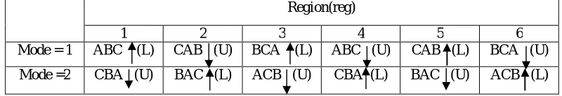
TABLE II: Rule of the determination of switching sequences (second mapping).
Region(reg)
1 2 3 4 5 6
Mode = 1 ABC (L) CAB (U) BCA (L) ABC (U) CAB (L) BCA (U)
Mode =2 CBA (U) BAC (L) ACB (U) CBA (L) BAC (U) ACB (L)
The variable reg is the region of the modulation triangle calculated in equation (8). Here the letter A, B, or C indicates switching states of phase A, B or C is to be modified sequentially. And the symbol “↑” or “↓” indicates that the state of the corresponding phase is increased or decreased by 1, respectively. For example, if the first switching state of a switching sequence is SaSbSc and the switching sequence rule is “ABC↑(L)” (i.e., reg = 1 and mode = 1) according to
Table II, then the switching sequence is generated as SaSbSc→ (Sa + 1)SbSc → (Sa + 1)(Sb +1)Sc → (Sa + 1)(Sb +1)(Sc
+1). The redundant switching states at each vertex are listed decreasingly from top to bottom corresponding to the switching states of phase A, of the space vector diagram, as shown in Fig 2[5]. For example, the switching states 566, 455, 344, 233, 122 and 011 at vertex P4 are listed decreasingly from top to bottom corresponding to the switching states
of phase A. The letter “L” in the parentheses represents the word “lower” and means the first switching state at the first vertex of the modulation triangle should not be the top one [5], e.g., not 566 for vertex P4; and the letter “U” in the
parenthesis represents the word “Upper” and means the first switching state at the first vertex of the modulation triangle should not be the bottom one, e.g., not 011 for vertex P4. Based on the second mapping, the switching sequences for the
reference vector in Fig. 2 according to different switching sequence modes are summarized in Table III and shown in Fig 3(b) and (c), and the accuracy of the switching sequences can be verified by comparison with the space – vector diagram is shown in Fig 2.
Table III: switching sequences for different modes
Mode = 1 162→161→061→051
Mode = 2 051→061→161→162
Consider “CAB↓(U)” when reg = 2 and mode = 1 [shown in Fig 3(b)] as an example to explain the switching sequence selection method in this paper. As mode = 1, reg = 2, the switching sequence is V0 →V1 →V2→V0. From V0 to V1, the
change of the vector is Vdc . ℮jπ/3, which can be substituted into equation (1) and means that the switching state of phase
C is decreased by 1. Similarly From V1 to V2, the change of the vector is Vdc.℮jπ, and from V2 to V0 the change of the
vector is Vdc . ℮j5π/3which can be substituted into equation (1) and means that the switching states of phase A, B are
For any level and reference vector with any modulation indexes, the second mapping is suitable and it can be extended to meet other requirement that is symmetric switching sequences. Based on the second mapping when the modulation index is low, the SVPWM scheme can generate more than one switching sequence [5].
Based on second mapping all the redundant switching sequences and optimal switching sequences for different applications can be easily generated. The optimized switching sequences, for example, achieving minimum number of switching transitions in a fundamental cycle as described in [4] can be obtained by simply choosing the first switching state of a switching sequence as that closest to the last switching state of the previous switching sequence. Moreover, because different switching sequences have dissimilar effects on the voltage across the DC link capacitors of a multilevel inverter [3], [6], [7], the SVPWM scheme provides more flexibility for balancing the dc – link capacitor voltages.
It should be noted that the second mapping in Table II is for generating the continuous switching sequences (i.e., no switching state is eliminated). The second mapping can also be conveniently modified to produce discontinuous SVPWM patterns (i.e., eliminating either the first or last switching state in each switching sequence), since discontinuous SVPWM can potentially increase the switching frequency and thus provide harmonic benefits for certain modulation ranges. For example, if the discontinuous pattern DPWMMAX is desired for the reference vector Vref
shown in Fig 2, the modulation rule for reg =2 and mode = 1 is adjusted to “CA↓(U)”, and the corresponding
discontinuous switching sequence is 162 → 161 → 061, which means phase B is un modulated. The rules for other discontinuous patterns can be summarized in a similar way.
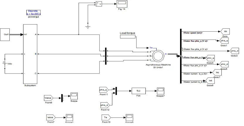
VI. SIMULATION MODEL OF SVPWM WITH INDUCTION MOTOR CONTROL
The simulation results are given for the induction motor as shown below. The specifications of the induction motor are: Number of poles (P) = 4, Frequency (f) = 50Hz, number of phases = 3, stator resistance (Rs) = 4.67Ω, Rotor resistance
(Rr) = 8Ω, stator inductance (Ls) = 347mH, mutual inductance (Lm) = 366mH, moment of inertia(J) = 0.061kg-m/sec.
Fig 6: MATLAB Simulink model of SVPWM based induction motor
Fig 7: MATLAB SIMULINK subsystem model for generation of pulses
In this SIMULINK the step by step procedure is as follows:
First the three phase voltages are calculated.
Vα and Vβ are calculated. For this 3ϕ to 2ϕ transformation block is used.
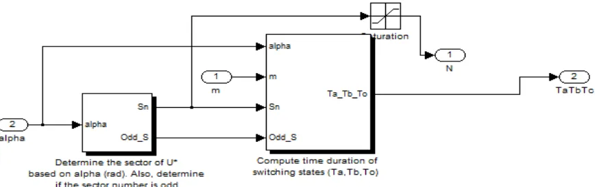
Now Vref and alpha are calculated, For this Cartesian to polar block is used.
compute the time duration of switching states Ta Tb Tc are calculated and Tn calculated (SV Modulator is
Shown)
Multiport switch is used for realisation of switching states (subsystem 2 is shown)
Finally, the 6 individual gate pulses for 7 level Inverter is derived (Subsystem 3shows).
Fig 8: MATLAB SIMULINK subsystem model for computing time duration of switching states
VII. SIMULATION RESULTS
In this simulation, the switching frequency fs is 1 KHz and fundamental frequency is 50Hz. And the modulation index
Fig 9: Normalized PWM waveform of the output voltage of 7 – level inverter
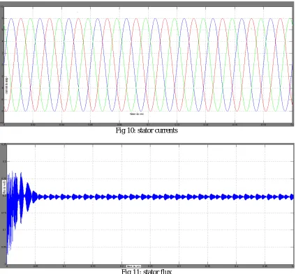
The results for the stator currents and flux are shown in figures (10) and (11) respectively.
Fig 10: stator currents
VIII. CONCLUSION
In this research paper induction motor speed control using space vector pulse width modulation is designed through MATLAB software and also tested successfully by evaluating the parameters like voltage, stator current, and flux. It is due to its characteristics like good power factor, extremely rugged and high efficiency. This scheme provides all the available switching states and switching sequences based on two general mappings and calculates duty cycles. This scheme also leads to be able to adjust the speed of the motor by control the frequency and amplitude of the stator voltage, the ratio of stator voltage to frequency should be kept constant. Besides the design and implementation of an induction motor using by MATLAB Simulink is trouble free and uncomplicated.
REFERENCES
1. N. Celanovic and D. Boroyevich, “A fast space vector modulation algorithm for multilevel three phase converters,” IEEE Trans. Ind. Appl.,
vol. 37, no. 2, pp. 637–641, Mar./Apr. 2001.
2. Gupta and A. Khambadkone, “A space vector PWM scheme for multi-level inverters based on two-level space vector PWM,” IEEE Trans.
Ind.Electron., vol. 53, no. 5, pp. 1631–1639, Oct. 2006.
3. Y. Deng, K. H. Teo, and R. G. Harley, “Generalized DC-link voltage balancing control method fo multilevel inverters,” in Proc. IEEE
Appl.Power Electron. Conf. Expo., Mar. 2013, pp. 1219–1225.
4. P. McGrath, D. G. Holmes, and T. Lipo, “Optimized space vector switching sequences for multilevel inverters,” IEEE Trans. Power Elec-tron.,
vol. 18, no. 6, pp. 1293–1301, Nov. 2003.
5. Y. Deng, K. H. Teo, Chunjie Duan A Fast and Generalised space vector modulation scheme for Multilevel Inverter, VOL. 29, NO. 10, oct 2014
6. M. Saeedifard, R. Iravani, and J. Pou, “Analysis and control of DC-capacitor-voltage-drift phenomenon of a passive front-end five-level
con-verter,” IEEE Trans. Ind. Electron., vol. 54, no. 6, pp. 3255–3266, Dec. 2007.
7. H. Zhang, S. Finney, A. Massoud, and B. Williams, “An SVM algorithm to balance the capacitor voltages of the three-level NPC active power
filter,” IEEE Trans. Power Electron., vol. 23, no. 6, pp. 2694–2702, Nov. 2008
8. Tripathi, A. Khambadkone, and S. Panda,“Direct method of over modulation with integrated closed loop stator flux vector control,” IEEE
Trans.Power Electron., vol. 20, no. 5, pp. 1161–1168, Sep. 2005.
9. H.Zhang and A. Von jouanne, S. Dai, A.K.Wallace and F.wang, “ Multilevel Inverter modulation schemes to eliminate common mode
voltages”, IEEE Trans.Ind. Appl., no.6 pp. 1645-1653, nov/dec 2000.
BIOGRAPHY
Mr. P.Raju received his B.Tech degree from sri venkateswara college of Engineering and Technology, Andhra Pradesh in 2013 and currently pursuing M.tech in Aditya institute of Technology and Management(Autonomous), Tekkali, Andhra Pradesh.His areas of interests include power system Analysis, Electrical Machines, Power Electronics and Drives.
Mr. S.Nagaraju received his B.E degree from AU college of Engineering, Vishakhapatnam in 1998 and received M.tech in Energetics in 2000 from Calicut University. Currently he is pursuing his Ph.D in AU college of Engineering, Vishakhapatnam. He had a teaching experience of 15 years. He had published many papers in different journals and conferences. His areas of interests include power system Analysis, Electrical power distribution and Electromagnetic field theory.