Capacitive Sensor with Transducer Using
Frequency Modulation for Seismometer
Rambolamanana Mamiharijao 1*, Andriatsihoarana Harlin2, Rambolamanana Gérard 3, Eddy Rasolomanana
4
, Razafiarisera Ralay Tiana 5
P.G. Student, Laboratory of Maintenance and Instrumentation, IOGA, University of Antananarivo, Madagascar 1* Professor, Electrical engineering Department, High Polytechnical School, University of Antananarivo 2
Full Professor, Institut Observatoire et Géophysique d’Antananarivo (IOGA), University of Antananarivo, Madagascar3 Full Professor, Mining Department, Geoscience Laboratory High Polytechnical School, University of Antananarivo4
P.G. Student, Laboratory of Maintenance and Instrumentation, IOGA, University of Antananarivo, Madagascar 5 * Corresponding author
ABSTRACT: Among the multitude of sensors, the capacitive sensor is one of the best to detect the displacement. Several kinds of vibrations sources may cause destruction of the civilian infrastructure such as earthquakes, explosions… To study seismology or seismic prospection needs an adequate sensor. A capacitive sensor design is proposed. The sensor used a pendulum system. One of the two capacitor plates is joined to the fixed holder, and the other one is joined to the mobile element. The vibrations detected are converted into electrical signal by using a transducer. The transducer is based on using frequency modulation (FM) system. A CMOS circuit phase locked loop is used for the transducer circuit base.
KEYWORDS:Transducer, frequency modulation, seismometer, capacitive sensors, PLL. I. INTRODUCTION
In seismometer, the signal period to detect an event can be over 100 seconds [9]. Our new seismic broadband sensor uses the capacitive sensor technical. Therefore, the frequency modulation is used for the transduction system with a variable capacitor. One of the two plates is joined on the fixed holder; the other one is linked on the mobile unit with the seismic mass (pendulum).
The previous system uses the capacitance variation of a variable capacitor [10]. A high frequency (HF) alternative signal with opposition phase is applied on the two plates fixed on the built. A mobile plate moves between the fixed plates. The phase of the resultant signal is picked out for the measurement [8].
II. RELATEDWORK
II-1- CAPACITIVE SENSOR
A capacitive sensor is a device that two conductive plates are separated by a small distance [1]. If a current flows, a positive charge q will be collected on the one plate of the capacitor. A balancing charge will be present on the other plate to preserve the neutrality charge. A voltage potential proportional to q appears between the two plates. =
Where A is the area of the plates, d is the distance of their separation, ε is the permittivity of insulating layer (ε0
=8.85pF/m for vacuum). The quantity = is the capacitance of the capacitor measured in Farads (F). The charge
= [1] [2].
II-2- THE MODULATOR
The modulating signal modifies the carrier frequency in modifying the signal phase [11]. It uses the frequency modulation technical: The carrier amplitude still constant then the frequency varies with the modulating signal rhythm [12].
The frequency modulated signal expression is [12] [13] [14]:
( ) = cos[ + 2 ( ) ]
u(t) is the modulating signal, k the modulator sensitivity expressed in Hz/Am (Ammodulating signal amplitude), ωp the
carrier instantaneous frequency. The instantaneous phase:
Ø( ) = + 2 ( )
If the modulating signal is a sinusoid, the carrier instantaneous phase is:
Ø( ) = +
Where ωm is the instantaneous modulating signal frequency. The instantaneous frequency
( ) = + . cos
The frequency deviation
∆ ( ) = .
The phase deviation or modulation index
∆Ø = ∆ =
The modulator is composed by the PLL Voltage Controlled Oscillator (VCO) (CD4046) and the capacitor C1 is
composed by two plates described above.
Figure 1: CD4046 circuit schema (4046 datasheet [5] [7]). It contains the VCO and three phase comparators.
II-3- THE TRANSDUCER
The function of this module is to extract the modulating signal. We use the synchronic detection technical. This technique consists to generate a signal with the same frequency and phase as the carrier signal. An intermediate signal is obtained by the product of the generated and the carrier signal. To get the modulating signal, the intermediate signal is filtered by a low pass filter [13] [15] [17].
If s(t) is the signal modulated by u(t):
( ) = [1 + ( )]. . cos
The intermediate signal is:
( ) = ( ). cos = [1 + . ( )]. .1 + cos 2 2
After filtering with low pass filter, the term with cos 2ωp will be eliminated, only the term with u(t) still remain.
Consequently, the carrier signal and the generated signal must be rigorously in phase. With the PLL system, we can synthesize a signal rigorously in phase with the carrier signal.
In figure 2, we can find the PLL synoptic. There are three functional blocs: A phase comparator, a low pass filter, a VCO. The phase comparator output voltage is ur, the result of ue and us phases shifting. This signal (ur) is filtered by a
low pass filter to get uf. The VCO voltage control is uf.
Figure 2: PLL synoptic composed by a phase comparator, a low pass filter, a VCO.
- Phase comparator:
Every time, this module compares the instantaneous phase φe of a periodic signal on its input with the VCO signal
instantaneous phase. The output delivers an average signal dependant of the phase shift between the two signals in input [14] [16]. The PLL is locked when fe = fs. The output voltage expression is [17]:
= . ( , )
KD is the comparator gain in V/rad.
- Low pass filter:
The harmonic signals present on the output must be eliminated by a low pass filter. An average signal will be covered. Only the direct current (DC) signal is covered [13] [15] [16].
- VCO:
The VCO runs at a set frequency f0 called center frequency when there is no signal input ue(t). When an input signal
ue(t) is applied, the comparator compares the phases and the frequencies of the input signal ue(t) and the signal
delivered by the VCO us(t). An error voltage ur(t) is generated and proportional to the phases and the frequencies
difference of the input and VCO signal. An average signal uf is delivered on the low pass filter output; it is applied to
the VCO control voltage. The signal uf(t) is used to reduce the frequencies difference [3] [6].
The frequency lock range is defined with the VCO characteristic shown in figure 3. The centre frequency f0
corresponds to = ; the frequency locked range is defined with 2 = ( − )[3]. The offset frequency is = − 1.6 [5].
The figure 3 shows the VCO frequency characteristic operating with offset. The center frequency is f0, corresponding
with Vcc/2. The frequency lock range is 2fL = (fmax – fmin), where fmax corresponds to VCOin = (Vcc – 0.9V) and fmin
corresponds to the VCOin = 0.9V, offset frequency is foff = f0 – 1.6fL [5].
Figure 3: VCO frequency characteristic (74HC/HCT4046 datasheet Philips) [5]. It presents the VCO frequency vs VCO in (voltage control)
The figure 4 presents two charts using to determine the PLL components. To select R1, R2, C1, give f0 and 2fL, R2 and
The CMOS circuit CD4046 is used as demodulator. The figure 1 shows the electronics assembly for the CD4046 [5] [7].
The signal input uses as reference is a signal stabilized by quartz. It is applied on the pin 14. We use the XOR gate for the phase comparator. The modulating signal is covered at pin 10.
III.SENSORDESIGN
A mechanical system supports the capacitor plates. One plate is fixed on the mobile element and the other one mounted on the immovable element. A displacement (d) between the two plates produces a variation of the capacitance( = ) [1]. This capacitor is coupled to the CMOS 4046 PLL circuit. It is used as C1 in figure 1. A
displacement variation produces a VCO frequency variation. On the input signal (pin 14 CD4046) is applied a reference signal by a quartz oscillator. When the PLL is locked to the reference signal, the pin 10 (Vdemod) provided a
demodulator voltage output of the VCO input. This signal is used to reduce the frequencies difference between the input signal (pin 14) and the VCO frequency [3]. The displacement variation of the mobile plate will be interpreted with the demodulation signal output variation.
The characteristics of the sensor are exposed in the next part: Sensitivity (modulator and transducer), modulation index, time response.
IV.EXPERIMENTAL RESULTS
- Sensitivity
The figure 5 shows the modulator response frequency (kHz) with respect to the displacement (mm). On the figure 5 (a) the response on the displacement range between [0.2; 3.0] mm is shown. On the figure 5 (b) the displacement range [0.2 ; 1.0] mm is considered. In this range the sensitivity is better (31.12kHz/mm).
(a) (b)
Figure 5: Sensitivity VCO frequency vs displacement. In (a) is presented the sensitivity with the full scale displacement, in (b) is selected the displacement zone where the sensitivity is better [0.2 ; 1.0] mm
The figure 6 shows the transducer demodulation (V) with respect to the displacement (mm). On the figure 6 (a), the demodulation versus displacement response between [0.5; 3.0] mm is represented. The figure 6 (b) represents the demodulation versus displacement response in the range [0.5; 1.0] mm. In this range, the sensitivity is better and the response is linear.
80 90 100 110 120 130 140
0 1 2 3
Fr e q u e n cy (k H z) Displacement (mm)
y = 31.12x + 94.56
80 90 100 110 120 130 140
0 0.5 1 1.5
(a) (b)
Figure 6: Curve representing the demodulation (V) vs the displacement (mm). In (a) is presented the sensitivity with the full scale displacement, in (b) is selected the displacement zone where the sensitivity is better [0.2 ; 1.0] mm
By regression:
( ) = 31.12 + 94.56 ( ) = −5.966 + 6.568
In these equations, d is in mm and f in kHz: the modulator sensitivity is expressed in Hz/m, and the transducer sensitivity in V/m, then:
= 31.12 . 10 / = 5966 /
- Modulation index
∆Ø = ∆ =
With the value range [0.5 ; 1.0] mm, the minimum displacement is = 0.5 , corresponds to = 110.12 , the maximum displacement is = 1.0 , corresponds to = 125.68 , then = 7.78 . The maximum modulating signal frequency is = 100 (see below). Then the modulation index is = 77
Carson relation gives the spectrum band width: = 2 (1 + ). [13] [14] With the above values = 15 600
We get a wide band modulation (WBM).
The displacement = 0.5 corresponds to the demodulation = 3.585 , the displacement = 1.0
corresponds to = 0.602 . The maximal amplitude of the modulating signal is 2.983 V peak to peak. - Time response
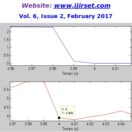
The figure 7 shows the transducer time response. Above is represented the command signal, below we can find the transducer response. The time response is the difference of the end of the time signal output and the end of the command.
0 2 4 6
0 1 2 3
D e m o d u la ti o n (V o lt ) Displacement (mm)
y = -5.966x + 6.568 0
2 4 6
0 0.5 1 1.5
Figure 7: Above the signal command, below the transducer response
Considering the figure 7, the time response is 0.01s. The modulating signal frequency cannot be over 100Hz.
V. CONCLUSION
- Two linear zones could be considered. The first is in the range [0.5; 1.0] mm, the second zone is in the range [1.2; 2.8] mm. The first zone presents the best sensitivity. It will be used for the sensor.
- An amplifier with a low noise and a gain equal to 13.4 is needed to get the same sensitivity as STS1 sensor sensitivity (80.000 V/m) [8].
- The time response knowledge is necessary because it limits the modulating signal frequency.
REFERENCES
[1] Mr.K.Sathesh, Dr.N.J.R.Muniraj, T.Divya Bharathi, S.Priyadarshini, S.Sharmila, “ Modeling and Simulation of Capacitive Pressure Sensor Using Comsol Multiphysics for Intraoral Applications”, International Journal of Innovative Research in Science Engineering and Technology (IJIRSET), Vol. 3, Issue 4, p 151-152, April 2014.
[2] Professor K. E. Oughstun “Capacitance”, School of Engineering College of Engineering & Mathematical Sciences University of Vermont, EE 141 Lecture Notes, Topic 15, pp. 11-13, 2014
[3] David K Morgan , “CD4046B Phase Locked Loop: A versatile building block for micropower digital and analog applications”, Texas Instruments, Application report, Scha002a, pp. 3-15, February 2003,
[4] W. M. Austin –: “CMOS Phase Locked Loop Applications using the CD54/74HC/HCT4046A and CD54/74HC/HCT7046A”, Texas Instruments, Application report, Scha003b, pp. 8-12, September 2002
[5] Philips Semiconductors, “Datasheet 74HC/HCT4046A – Phase Locked Loop with VCO”, pp. 6-26, November 1997 [6] G. Couturier, “ Boucle à Verrouillage de Phase et Applications”, Département GEII IUT Bordeaux I, Vol. 9, pp. 11-14 [7] NXP Semiconductors, “HEF4046B – Phase Locked Loop”, pp. 2-11, March 2016
[8] Robert Pillet, “Cours sismométries- Chapitre 4”, Geoazur, pp. 6-7, Mars 2013
[9] Villard de Lans, “Cours de sismométrie – La mesure en sismologie”, EOST Université de Strasbourg, pp. 5-8, Novembre 2014
[10] Rubhini .B, Vijay Antony Raj.B, “ Electrical Conduction Behaviour of The Cement Matrix Composite with Wireless Intelligent Sensor Network and Embedded Piezo Transducer in Concrete for Automatic Structural Health Monitoring in Bridge Structures”, International Journal of Innovative Research in Science Engineering and Technology (IJIRSET), Vol.3, Issue 8, pp. 15532-15533, August 2014
[11] Launay Frédéric, “Cours modulation analogique”, Laboratoire d'Informatique et d'Automatique pour les Systèmes (LIAS), pp. 30-35 [12] Jean Philippe Muller, “La modulation de fréquence”, Physique appliqué, TA Formation, pp. 3-6
[13] A. Dupret, A. Fischer, “Cours de télécommunication”, Université Paris XIII, IUT de Villetaneuse, Département Génie Télécommunication et Réseaux, pp. 11-23 [14] Desmoulière Jean-Baptiste, Chevillard Christophe, “La modulation de signaux analogiques et la boucle à verrouillage de phase dans les télécommunications AC20”,
Université de Technologie Belfort-Montbéliard (UTBM), pp. 11-14, 2004
[15] M. Correvon, “Systèmes électroniques – Boucle à verrouillage de phase”, Institut d’Automatisation Industrielle, Haute Ecole Spécialisée de Suisse Occidentale (Hes.so), pp. 1-16
![Figure 1: CD4046 circuit schema (4046 datasheet [5] [7]). It contains the VCO and three phase comparators](https://thumb-us.123doks.com/thumbv2/123dok_us/1617641.1200840/3.595.186.411.158.344/figure-circuit-schema-datasheet-contains-vco-phase-comparators.webp)
![Figure 3: VCO frequency characteristic (74HC/HCT4046 datasheet Philips) [5]. It presents the VCO frequency vs VCO in (voltage control)](https://thumb-us.123doks.com/thumbv2/123dok_us/1617641.1200840/4.595.130.481.592.751/figure-frequency-characteristic-datasheet-philips-presents-frequency-voltage.webp)
![Figure 5: Sensitivity VCO frequency vs displacement. In (a) is presented the sensitivity with the full scale displacement, in (b) is selected the displacement zone where the sensitivity is better [0.2 ; 1.0] mm](https://thumb-us.123doks.com/thumbv2/123dok_us/1617641.1200840/5.595.89.508.493.637/sensitivity-frequency-displacement-presented-sensitivity-displacement-displacement-sensitivity.webp)
![Figure 6: Curve representing the demodulation (V) vs the displacement (mm). In (a) is presented the sensitivity with the full scale displacement, in (b) is selected the displacement zone where the sensitivity is better [0.2 ; 1.0] mm](https://thumb-us.123doks.com/thumbv2/123dok_us/1617641.1200840/6.595.85.513.170.330/representing-demodulation-displacement-presented-sensitivity-displacement-displacement-sensitivity.webp)