George C. Hwa
Center for Communications and Signal Processing Electrical and Computer Engineering Department
North Carolina State University
ccsr-
TR-88/13HWA, GEORGE C. Digital Communication System Design Workstation. (Under the direction of Sasan Houston Ardalan) The Purpose of this project was to design and implement an advanced Multibus-based multiprocessor workstation that could be used in digital communication system research. The workstation's bus-based archi-tecture enables it to survive technological evolutions in DSP hardware and algo-rithms. The architecture consists of a Multibus I system bus interface, a DB32016 single-board microcomputer, which is based on the 32-bit NS32016 microprocessor,
with a memory expansion unit and two TMS320 family-based DSP units along with data acquisition devices. The Multibus I system bus interface is the main communica-tion channel through which the bus master, DB32016, monitors and controls system
operations in the workstation. Digital signal processing tasks are performed by the
Table of Contents
Page
Chapter 1 Introduction 1
1.1 Digital Signal Processing.. 1
1.2 DSP in Power Line Communications 2
1.3 DSP Workstation Approach 3
1.4 Summary of Topics 4
Chapter 2 Motivations 5
2.1 Real Time DSP 5
2.2 Adaptations to New Technologies 8
Chapter 3 Proposed
nsp
Workstation Architecture 10 3.1 Bus-based System Architecture and Multibus-I/IEEE796 103.1.1 Multibus System Bus 11
3.1.2 Workstation Hardware Components and Their Function 12 3.2 General Purpose Microcomputer Sub-System 13
3.3 DSP Sub-System 14
3.3.1 TMS32010 and DSP32010 15
3.3.2 TMS32020 and DSP32020 18
3.4 Data Acquisition Sub-System 20
Chapter 4 Software and User Interface 23
4.1 DSP Program Development Tools 23
4.2 Basic DSP Routines 24
4.2.1 Sinewave Generator 24
4.2.2 IIR Filter with Normalized Lattice Structure 27
4.2.3 Nyquist Pulse Shaping 28
4.2.4 Random BitGenerator and A/D-D/A Interface 29
4.2.5 LMS Adaptive Filter 29
4.3 Workstation User Interface 31
4.4 TMS320 Simulator 31
Chapter 5 Application to Distribution Power Line Communications 33
5.1 Formulation of the Problem 33
5.2 Adaptive Harmonic Cancellation 34
5.3 Finite Precision Arithmetic 38
5.4 Digital Phase-Locked Loop 39
5.5 All Digital Communication System 43
Chapter 6 Summary of Achievements and Future Research 45
6.1 Summary of Achievements 45
6.2 Future Research 46
6.2.1 DLC Implementation 46
6.2.3 Additional Support Software 48 6.2.4 DSP Algorithm Implementations... 48
References... 51
Appendix A Digital Communication Workstation User Manual 58
Very-Large-Scale-Integration(VLSI) technology has experienced exponential growth in the past two decades. In an area less than a quarter of a square inch, a cir-cuit designer is now able to place over 100,000 gates to realize circir-cuits of tremendous complexity. An electronic circuit realizing a complicated system which had to be implemented with several boards ten years ago, it can now be integrated onto one small chip. In the process, the cost per gate of fabricating such a tiny chip has been reduced to a fraction of a cent. The benefits of this technological progress have been manifested in every branch of science and engineering fields. One of the areas that has received a great impact is Digital Signal Processing(DSP).
1.1 Digital Signal Processing
Digital signal processing techniques have been widely used in speech and image processing, digital communications, and advanced digital control systems[26][30][32-37][43]. The rapid advancements in both hardware(specifically microprocessors which make DSP possible) and software(algorithms which exploit DSP implementa-tions) make digital systems practical substitutes for their analog counterparts. Digital systems have the advantage of reliability, reproducibility, compactness, programma-bility, and efficiency.
meet exact design specifications without labor-intensive tuning. As the level of inte-gration continues to increase, digital systems are becoming more and more compact, enabling applications where space constraints are severe. Since the functionality of digital systems are primarily determined by the underlying software, the same hard-ware often can be re-configured to perform completely different functions by simply replacing the software. This programmability significantly reduces the time required to develop new systems, allowing system expansion and upgrading to take place at a much faster pace in order to keep up with the rapid development of advanced DSP algorithms. The improved efficiency is fully manifested in performance versus cost.
DSP applications have penetrated almost every area of science, engineering, and everyday life. In speech processing, DSP technology makes speech synthesis and recognition possible. Scientists in astronomy, geology, and meteorology are using DSP to interpret images to a greater extent. Engineers in the video industry are applying DSP technology to enhance the performance of video display equipment. In communications, all-digital radios are designed and built with DSP technologies. Par-ticularly in telecommunications, where DSP probably has the largest usage, it has become an essential technology.
1.2 DSP in Power Line Communications
transmissions. In addition, 60 Hz harmonic noises are so strong that high fidelity transmission is impossible without special treatment. Special techniques have been developed over the years to combat the hostile power line communication environ-ment[22]. These techniques rely heavily on the successful implementation of mathematical computation intensive algorithms. As DSP hardware improves with the improvement in VLSI technology and as new algorithms are developed, the existing communication systems quickly become obsolete. New techniques cannot be readily tested on existing hardware platforms, although computer simulations may be used for validation. In the meantime DSP system designers and researchers are seeking advanced development tools to shorten the development cycle and to keep up with the fast technological advancements.
1.3 DSP Workstation Approach
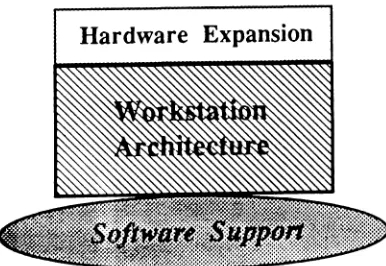
The aim of this project was to design and implement a DSP workstation with an advanced architecture, sophisticated software support, a user-friendly operating envi-ronment, and the flexibility for system expansion and upgrade. The workstation concept is illustrated in figure 1.1. The motivation for the workstation approach is
dis-Hardware Expansion
cussed in chapter 2. The DSP workstation has been utilized extensively in the study of power line communication systems which overcome the difficulties associated with power line communications.
1.4 Summary of Topics
Chapter 2 Motivation
The need for a DSP workstation, which can be used to quickly develop digital sys-tems, is obvious. Researchers need the workstation to verify the validity of DSP algorithm in real time without the concern for hardware implementation detail. Design-ers may use the workstation to confirm system designs and to improve such designs prior to the actual hardware construction. Given its flexible system architecture, the DSP workstation will enable researchers and design engineers to remain at the fron-tier technology. For instance, in order to explore the capabilities of a newly developed DSP microprocessor, which emerges every couple of years, the new DSP micropro-cessors can be incorporated into the workstation without altering the basic hardware structure and software environment of the workstation. This type of architecture allows researchers and design engineers to adapt to new technology quickly with min-imal effort.
2.1 Real Time DSP
DSP researchers often rely on computer simulations for verification of their research results. Computer simulation is a relatively inexpensive way to model the behaviors of physical systems. The simulation results, though not observable in real time, can be used to examine the correctness of an algorithm. Computer simulations save researchers the time and effort of building the actual hardware that implements
a particular algorithm. If the initial simulation results are not satisfactory, the
modified to model an improved version of the algorithm. Thus a researcher can go through the design process from a particular algorithm to the implementation(via sim-ulation) back and forth a number of times before reaching a conclusion about the algorithm. Researchers who are not familiar with building DSP hardware can still obtain an understanding of how algorithms will behave in physical settings. The major short coming is that computer simulations can only model a physical process for a rel-atively short real-time frame, i.e. the simulation results can only represent a short instance of a physical process. For example, a DSP algorithm is implemented in hard-ware to process a speech signal at an 8K Hz sampling rate. Then 480,000 samples have to be processed by the hardware in one minute of real time. From experience, it might take more than an hour of CPU time to simulate 480,000 samples on a VAX-lIn80 super mini-computer. If the simulation is performed on a multi-user system, which is normally the case, it may very well take an entire day before the results are available. Such a lengthy computer simulation is usually avoided due to the high cost of CPU time. Furthermore, data storage requirements may also be prohibitive.
case of computer simulation. It reduces researchers experimental efforts and increas-es dincreas-esign engineers productivity by allowing them to go through dincreas-esign cyclincreas-es quickly and easily. Of particular importance to the design engineer, a shortened time from the drawing board to prototype means a better product with less cost, since the designer does not solely depend on the results from computer simulations to make design deci-sions. The generality of the DSP workstation hardware allows a design engineer to explore his/her options in choosing necessary hardware components to implement a specific digital system and to use only those components that are needed for the sys-tem in the final product. The elimination of the prototype hardware construction phase can mean a significant savings in time and cost. Design engineers can make better design decisions without the concern for cost overruns in the design process. There-fore, the workstation offers the best of both computer simulation and hardware implementation approaches.
operations in computer simulation. The later alternative is usually a rather involved process that most people avoid whenever possible. Therefore, the former alternative, testing an algorithm with a true DSP processor, leads to another supporting argument for building the DSP workstation. Also worth mentioning is the fact that many DSP algorithms have critical timing requirements. Such behaviors are better understood by studying them is the real time.
2.2 Adaptations to New Technologies
In order for DSP researchers and design engineers to keep up with the rapid advancements in VLSI technology, which is one of the driving forces behind DSP tech-nology, a DSP workstation with hardware expansion and upgrade capabilities is desired. Instead of developing and replacing the entire DSP system every time a new DSP processor becomes available, or additional hardware features are needed to meet the more sophisticated DSP processing requirements, the enhanced DSP work-station architecture can be used to allow system expansion and upgrades. These features will give researchers and designers a leading edge in discovering advanced DSP algorithms and bringing about competitive DSP products. The workstation approach also makes the DSP research and development environment highly stable. Once an interactive and user-friendly programming environment is developed for the workstation, it will provide the user accesses to the workstation's resources in a con-sistent manner. This eliminates the overhead involved with the migration of research and design environments, and reduces the time and effort required to keep up with technological changes.
which efficiently employs advanced VLSI microprocessors with unique DSP capabili-ties, easily allows hardware expansion and upgrades, continuously accommodates a stable real-time digital signal processing environment, and genuinely provides a user-friendly programming interface. The workstation is to become a powerful research and design vehicle in DSP applications, specifically in power distribution line carrier
Chapter 3 Proposed DSP Workstation Architecture
The motivations and requirements discussed in chapter two lead to t1l' specifica-tions for the proposed workstation architecture. The overall workstation architecture calls for a bus-based multiprocessing system. Major hardware components of the workstation include a general-purpose microcomputer subsystem, dedicated DSP
General Purpose
Microcomputer
1
}~i;::.:;;~!~;::!l!l!fl~~illi!!!:~;"~---..I~
1
MultiBus I System Bus
Figure 3.1 DSP Workstation Architecture
microprocessor-based subsystem, and a data acquisition subsystem. The proposed architecture is illustrated in Figure 3.1. These subsystems are described in sections 3.1 to 3.4. Section 3.5 discusses the design, construction and testing of the worksta-tion hardware.
3.1 Bus-based system architecture and Multibus-IlIEEE796
the workstation components may be obtained from various sources other than doing custom design. In addition to the advantage of large variety of components available by using a standard bus, there is also the benefit of maintaining a stable overall con-figuration and programming environment as the workstation undergoes hardware upgrade.
There are a number of industry standard system busses that are intended for microprocessor-based system applications. Some of the bus architectures have been conformed to IEEE standards. Among those is the Multibus-I system bus, also known as the IEEE/796 Standard Bus. This bus has been chosen as the system bus for the DSP workstation.
3.1.1 Multibus System Bus
A Multibus memory access takes place during a memory cycle. A bus master places an address on the address bus lines. The addressed slave decodes the address and responds by sending an acknowledge signal back. Then the bus master issues a memory read/write command while data being transferred over the data lines.
A Multibus I/O access takes place during an I/O cycle. The process proceeds in similar fashion as in memory cycles except that the bus master issues I/O read/write commands instead of memory commands.
To facilitate system operations, i.e. bus cycles, there are special signals, including bus priority (BPRN), bus busy(BUSY), bus requestCBREQ), and inhibit sig-nals(INHI and INH2), designated in a Multibus system to enable or disable a device to initiate bus cycles.
The Multibus-I is chosen as the candidate for the system bus for several reasons. First, it is a well-defined industry standard as well as an IEEE standard. Second, there are a large number of Multibus compatible system components available. Third, the cost of building such a system is relatively inexpensive compared to other buses, such as Multibus-II and VME bussed which are synchronous bus interface systems.
3.1.2 Workstation Hardware Components and Their Functions
single-chip microcomputers with a Multibus compatible interface to allow the bus master to carry out necessary operations. The data acquisition devices, analog-to-digital(AID) and digital-to-analog(D/A), are not actually a part of the Multibus inter-face components. They are separately implemented and interinter-faced to one of the DSP units through two dedicated parallel ports. The analog acquisition system band-limits the incoming analog signal and samples at the Nyquist rate. The sampled data is transferred to the DSP units that perform desired DSP operations on the data. The processed data is then passed onto the D/A converter which converts the data back to an analog signal. A workstation user can control the operations by communicating to the bus master through a sophisticated user interface under software control.
3.2 General Purpose Microcomputer Subsystem
The workstation provides its powerful DSP capabilities to the users through a general purpose microcomputer subsystem along with an interactive user interface. The subsystem contains hardware elements that reside on two Multibus boards -the DB32016 single board microcomputer and -the PSM512A memory board.
host assisted mode to execute programs. The Multibus interface allows it to
commu-Multibus
Figure 3.2 Microcomputer Subsystem
nicate with other boards on the system bus. Off-board addressing includes both memory and I/O spaces. The PSM512A is a random access memory board with error checking-correction feature[78]. It provides an additional 256K of memory for the DB32016 through the Multibus interface. The DB32016 is configured as the bus mas-ter in the workstation, having access to all the workstation hardware sources - the memory on DSP units and the I/O ports mapped onto the Multibus I/O space.
3.3 DSP Subsystem
master to load programs and exchange data with the DSP subsystem. The two DSP
r---
--.-r---.-r-,~-',- - --:-.----.'7~':'--~ -~.-.~.':'~~:-. ~";"- .-r.-r--,:,--.- --- - - -~:r~~-~-;• ,'.: . :.:... I
I:::
.llllllllll!ll;i]
: : " ' ! " ' : : : : : : : : : '..
:!:::'!r>.·.· 4::::::· .:- >:.<.... :
C_· ..._... ... _.;;;_..:._.~..;...~!!.1:!~~'
__..';". _
_
.__....__;...
_.J MultibusFigure 3.3 DSP Subsystem
units are loosely coupled through a dedicated communication link, allowing them to exchange information while executing independent tasks.
3.3.1 TMS32010 and DSP32010
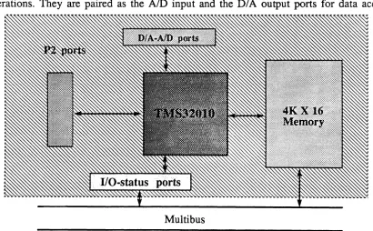
The DSP32010 board uses a TMS32010 microprocessor chip, TI's first generation DSP microprocessor family, as the CPU. The TMS32010 is interfaced to the dual-ported memory and the I/O devices.
XI
ClKOUT X2/CLKIN
... . - . - 015·00
SHIFTEn (0·1~) INSTnUCTION DATA pnOGnAM nus 10 AnOllO)I An1 (10) I
DATA RAM (144x10)
CI)
r - - - t - - - -__--I~(I)
w a: a o ct a: UJ
...
-' o a: t-Z o u LEGEND: Ace. AccumulatorAn? Auxiliaryraglstorpointor ARO. Auxiliary rogls tor 0
An1 - Auxiliary reoistor 1
OP • Data paoopolntor
PC • Prooram countor • P • P roolstor
T • T roo'stor
WE DEN MEN iiiO MC/MP INl ftS A11·AO/ PA2·PAO
is a four-level stack for context switching.
The DSP32010 board provides 4Kx16 static memory with 45ns access time to allow the TMS32010 to execute instructions at full speed. The memory is also mapped onto the Multibus memory space to allow direct access by the bus mas-ter(DB32016). Since there is no way to temporarily suspend the program executions on the TMS32010, the only way the DB32016 can access the dual ported memory is to halt the TMS32010 and reset it afterwards.
Six I/O ports are built into the DSP32010 board to facilitate the TMS32010's I/O operations. They are paired as the AID input and the D/A output ports for data
acqui-Multibus
Figure 3.5 Functional Block Diagram of the DSP32010 Board
3.3.2 TMS32020 and DSP32020
The second board, the DSP32020, implements TI's second generation DSP micro-processor chip, the TMS32020 as the CPU. The board was built with a dual-ported memory and 110interfaces.
In addition to the features contained in the TMS32010, the TMS32020 has the increased on-chip memory capacity(from 144x16 to 544x16) and the increased pro-gram and data memory spaces(both up to 64Kx16). The new processor also increases number of I/O ports up to 16 ports. It has the ability to interface with low speed exter-nal memory chips and the ability to configure the on-chip memory for storing either data or instructions, or both. Two serial I/O ports are added on the TMS32020. It also has a multi-level interrupt capability and an enhanced instructions set.
IfR(6) "PTCCO) 18 ItUl0) STO(10) 5T1(16) DXn{lGI TlMn 0) IMnIG) pnono) GneG{O) 18
, . - - - o n
r---
ClKR- - - F S R - - - . O X
cueX FSX ,."OGnAM bUS '0 1(; ,."OGllAM UUS 16 16 16 7 LSD FROM In 10 DATA IIUS 10 10 tc OAT RAM OLOCK 01 (258J( 181 3 3 ... IU I~I~J~ ~ 16 RNi Sfiiii READY iii XF
m
HOLDA M'SC iiiO RS lACKINT(2·0J
-A 15·-AOof--rl"--t
01(;·00
HOLD signal is removed to allow the TMS32020 to continue its execution.
There are four 110 ports on the DSP32020, paired as the Multibus I/O ports and the P2 lIO ports. The P2 I/O ports are connected to the DSP32010, providing a private
Multibus
Figure3.7 Functional Block Diagram of the DSP32020 Board
link between the two
nsp
units. A four level interrupt register allows the bus master toperform multi-level interrupts to the TMS32020 on the DSP32020.3.4 Data Acquisition Subsystem
the digital signals to be processed and the analog signals in the real world environ-ment.
3.5 Hardware Design, Construction and Testing
The major hardware design, construction, and testing efforts were devoted to DSP sub-systems and were carried out in two stages. The DSP32010 board was designed and constructed first to gain familiarity with the Multibus interface. The DSP32010 board is designed with a minimum set of requirements to interface with the Multibus interface as a slave processor. These requirements are (1) Multibus address decod-ing, (2) Multibus memory and I/O command recognitions, and (3) command acknowledge signal generation. These features enable the board to be configured into the Multibus system as a slave processor. The design of the TMS32010's memory and I/O interfaces are relatively straight forward. The DSP32010's Multibus interface circuitry and its dual port memory are tested by the bus-master DB32016. After-wards the bus-master loads the dual port memory with testing routines executable by the TMS32010 and flags it to perform expected functions. The DSP32010 is then connected to the data acquisition sub-system through the I/O ports PA5 and further real-time testing are conducted with test instrument observable results. A TMS32010 emulator was employed during the hardware debugging phase.
provides signals to access slower memory devices(not possible with the TMS32010). However, this feature is not implemented on the DSP32020 board to access slower speed devices. Rather the feature is used to enable the DB32016 to suspend the pro-gram execution on the TMS32020 while the DB32016 is accessing the dual port memory through the Multibus interface. During the TMS32020's program execution no wait state is necessary to access the fast static memory.
The two boards were constructed using half-height Multibus boards with the quick-connect technique for component connections. The quick-connect technique is similar to the wire-wrap technique, requiring no component-connection soldering. However, boards constructed using the quick-connect technique have lower board-heights compared with boards using the wire-wrap technique. The space constraint on a half-height Multibus board results two separate boards to house the TMS32010 and the TMS32020.
High speed(access time under 50ns) static memory chips are used on both the DSP32010 and the DSP32020 boards for simplicity of circuit design and full-speed execution of the TMS320s. Dual ported latches are used for the Multibus I/O ports and the P2-I/O ports. Therefore, transferring data on these ports must be synchro-nized by both input and output sides to ensure that no data is lost during the communication process.
Chapter 4 Software and User Interface
Advanced software is required to make efficient use of the workstation for DSP applications. The software tools discussed in this chapter enable the user to quickly translate DSP algorithms into programs executable on the workstation's DSP hardware. A user friendly interface makes the workstation operations transparent to the user. Program execution, control, and debugging on the workstation are as easy as on the host computer system.
4.1 DSP Program Development Tools
The variety of development tools available to the workstation enables the user to write programs in different languages and at different levels. The high level language programming makes program development fast and reliable while the lower level programming environment provides the user easy access to the various workstation's hardware resources. There are assemblers available for the TMS320s and the DB32016. And the Cprogramming language is available for the DB32016.
To develop programs for the DB32016, the user writes most routines in the C. For hardware dependent tasks, assembler routines must be written to interface to the specific hardware components in the workstation. After the C source is compiled and the assembler codes assembled, these modules are linked together to a form executable image to be loaded into the DB32016. The DB32016 assembler and the C compiler, along with the linker, are available on a VAX host computer under the UNIX operating system.
uses the assembler to translate the source into machine code. The macro-assembler, developed at the North Carolina State University[74] , is a powerful assembler with an enhanced macro facility. The macro facility allows the user to write compact source programs and generate in-line codes for fast execution. The macro-assembler itself is written in the C and has been ported to UNIX, DOS, and VAX-VMS systems. The output format of the assembler is Intel checksum ASCII records. The records are easily transportable between systems and can be readily loaded into the workstation's DSP units.
4.2 Basic DSP Routines
To facilitate DSP program development, some basic DSP operations/algorithms are coded into subroutines/macro-definitions and can be easily incorporated into application programs. They are sinewave generator, IIR filter, Nyquist pulse shaping, random number generation, A/D-D/A interfaces, and LMS adaptive filter.
4.2.1 Sinewave Generator
the sinewave generator. Therefore, using the TMS32010 the program memory is used for table storage. These table values can be read into the registers by the TBLR instruction. In contrast, the TMS32020 has a large data memory space - up to 64K words. Therefore the table can be directly stored in data registers, eliminating the TBLR overhead.
The second method requires two tables, the first one, a coarse table, contains samples of a unit circle and the other, a fine table, contains values uniformly sampled between two samples of the first table.
Let
a=8+o
using the trigonometric identity
sintci) =sin(8) cos(8) +sin(8) cos(8)
(4.1)
(4.2)
and let
e
denote the coarse table angle and8
denote the fine table angle. If8is chosen to be sufficiently small, thencostb)
~ 1Therefore, (4.2) can be approximated by
siniti) ~sin(8) +sin(8) cos(8)
Furthermore,
(4.3)
(4.4)
cos(S)
=
sin(S+1t/4) (4.5)Thus sin(S) and cos(S) can be found in the coarse table and sin(O) can be found in the fine table. The final result is obtained by one multiplication and one addition. The overall resolution of the implementation is
21t
N·n
whereN and nare coarse and fine table sizes, respectively. The frequency resolution.j', can be computed by
.s.
!,
=N· n
where F
s
is the sampling frequency of the system. The table sizes are chosen as follows. Since21t °max-<
N
we chooseN such that
in the fixed-point arithmetic. LetN
=
1024. Then0max< 0.0061359231
and cos(Omax) >cos(0.0061359231) = 0.999981175274
(4.7)
(4.8)
(4.9)
(4.10) (4.11)
Therefore the right hand size of (4.11) is rounded to 1 using a 14-bit fixed-point arithmetic. This implies that (4.4) becomes
sinisi)= sin(S) +sin(O) cos(S) (4.12)
The choice of the fine table size n is then just a matter of meeting the desired frequency resolution.
The tables are generated with a program written in C. These table values are computed with floating point arithmetic for high accuracy, then they are quantized to 14-bit integers. The program can be executed on the host computer and then the table values are assembled into the TMS320 routine. The TMS320 routine is then loaded into the program memory. However, the DB32016 can also be used to generate the sine table values and directly load the table into the TMS320's memory at run-time. This means the table size can be changed dynamically to meet application's requirements.
Use of the sinewave generator is accomplished via a subroutine call by passing an angle
a
through the accumulator. The anglea
is a 17-bit integer, which is decomposed into 8(10 bits) and 0(7 bits) by the subroutine. The corresponding table value is returned in the accumulator to the calling routine. The frequency can becomputed by
F
s
f= .
a
N· n
4.2.2 IIR Filter with Normalized Lattice Structure
(4.13)
The infmite-impulse-response(IIR) filters are implemented using a normalized lattice structure. A single lattice structure is coded as a macro definition. The user designs a filter and converts the filter coefficients to second order pairs. These coefficients and the order of the filter is then given to the filter subroutine to be
accumulator as well.
4.2.3 Nyquist Pulse Shaping
Nyquist pulse shaping is accomplished by using a raised cosine envelope to shape the data pulse. The raised cosine envelope is sampled in the time domain and symmetrically truncated to five periods, with two periods each at both sides of the
10 dBM
-70 dBM
10KHz
Figure 4.1 Pulse Shaping with BPSK Modulation Spectrum of a Real-Time Signal
15 KHz
table to store the envelop data samples and the longer delays for data pulses.
Figure 4.1 shows the spectrum of a BPSK modulated signal with pulse shaping.
4.2.4 Random Bit Generator and AID-DIA Interface
The random number generator is implemented to simulate a random data source. It is implemented using fixed-point arithmetic with 16-bit precision. The routine saves a number called seed and uses it to generate the next random number with a new seed. The remainder operation is done by taking only the lower-order bits from the accumulator. The routine can be used to generate binary data, rather than arbitrary integers, to be encoded for transmission tests.
Because the AID and D/A data samples are in offset binary format and the TMS320s perform operations in two's complement, data samples must undergo the proper conversions. The AID-D/A interface macros make the conversion transparent to the user. The data samples received from the
AID
are fITst converted from offset binary to two's complement. After the samples are processed, they are converted back from two's complement to offset binary for the D/A to output.4.2.5 LMS Adaptive Filter
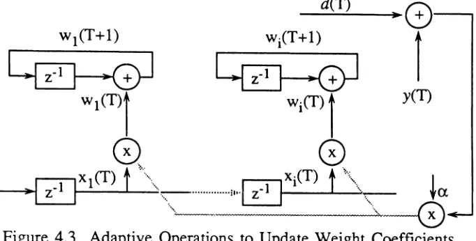
The adaptive filter is implemented as an LMS transversal filter structure. The filter produces anoutputy(T)from a weighted sum of delayed input samples.
y(T)
=
WT(T)·X(T) (4.14)filter coefficients. The transversal filter structure is illustrated in figure 4.2 .
...---~G
..· ···· ··..· ···
IIe .G---"·
I~~t
1
1
GoSrJ)
GlSrJ)
G~®
t---~
z _l:.~~tk
xO(T)
---~I
input
Figure 4.2 Transversal Filter Structure Let the error
e(T)
=
d(T) - y(T) (4.15)be the difference between the desired response and the filter output. The goal is to update W(T) periodically such that the error e(T) is minimized. By the LMS algorithm,
W(T+1)= W(T) +aoe(T)·X(T) (4.16)
where
a
is the feedback gain constant that affects the stability and the rate of convergence of the filter coefficients. Moreover,2
a<
<:
(4.17)where
A
maxis the eigenvalue of the input's autocorrelation function. The LMS adaptive operation is depictedinfigure 4.3.the filter. The macro assembler will generate in-line codes for a particular design.
d(T)
y(T)
Figure 4.3
The filter building block has been modified for the TMS32020, utilizing the available hardware resources to improve the performance. The filter uses TMS32020's auxiliary registers to perform looping control, eliminating the need for in-line code execution. TMS32020 has special instructions to perform looping control without adding overhead. These instructions are highly optimized for pipelining. By taking advantage of these advanced features on the TMS32020, the filter requires less program memory than the previous implementation. By using loop control to determine the size of the filter the implementation allows the user to alter the filter order after the program is assembled. Therefore, the user can change the order of the filter at run time, making it more flexible. Appendix B lists the assembler program source code that implements the adaptive filter on the TMS32020.
4.3 Workstation User Interface
are loaded into the workstation using the debugger. The execution control is accomplished through the monitor commands. The user can issue commands either to the monitor directly or to the host computer and let the debugger perform translations. Appendix A describes the detail of the workstation's operations.
4.4 TMS320 simulator
Chapter 5 Application to Distribution
Power Line Communications
The use of power lines as a transmission media poses some unique problems which have received considerable attention[22]. The major problem is the high noise level on the distribution lines. The noise appears mainly as 60 Hz based harmonics. An effective technique for combating this distortion has been studied and will be implemented on the workstation to demonstrate its feasibility. Other aspects of digital implementation of DLC are also discussed.
5.1 Formulation of the Problem
Applications of power line communication include load management, remote meter reading, distribution equipment monitoring and control, and possibly voice communications. These applications face the same type of threat as any other type of communication systems, primarily noise. The noise on the power lines comes from spikes induced by switching devices with various loads. These spikes are synchronous with the 60 Hz carrier, and appear as harmonics. The traditional approach is to transmit a signal with very limited bandwidth and to use fixed bandpass filters to remove the harmonics. However, with the 60 Hz carrier shifting over time and the bandwidth of the harmonics shifting, these fixed filters are often ineffectivee
filters in analog form is very costly if not impossible. With the dramatic reductions in DSP hardware costs, the implementation of adaptive filters has come within the reach of researchers and system designers. Integrating adaptive filters to perform harmonic noise cancellation in power line communication systems has become a practical solution to deal with the hostile environment.
Here we present how an adaptive filter implemented to perform harmonic cancellations in a digital receiver system. Typically, the incoming signal is first sampled at an appropriate sampling rate. The sampled data are bandpass filtered and demodulated to extract the baseband signal. Then the appropriate decimation is done to lower the sampling rate, followed by passing the data samples through an adaptive filter to remove the correlated 60 Hz harmonics before the final signal detection process.
The following sections discuss the building blocks of a digital communication system for DLC and the implementation issues involved.
5.2 Adaptive Harmonic Cancellation
wide auto-correlation function and is relatively easy to predict from the past samples. The delay queue de-correlates the broadband signal to allow the adaptive filter to predict only the narrowband signal.
Signal(broadband + narrowband)
Error (broadband)
Prediction (narrowband)
Figure 5.1 Adaptive Filter Structure
The incoming signal components consist of enccded data and 60 Hz harmonics. The encoded data component is such that it arprpteaJS 'as a broadband signal, i.e., it is highly un-correlated. The harmonics are obviously highly correlated. Therefore, it is possible to make a prediction based on the past samples of the signaL The prediction is a close replica of the narrowband signal, harmonics of 60Hz. Subtracting this predicted signal from the incoming signal, the data signal is obtained with improved signal-to-noise ratio.
execute looping instructions automatically. Highly optimized pipelining instructions can be executed faster than in-line code type of implementations. Furthermore the pipelined looping control implementation saves a large amount of program memory. Therefore the program can be loaded into the program memory much quicker. The test results, obtained by running the filter at8KI-Iz sampling rate, are shown in Figure5.2.
The adaptive filtering is to be performed after the demodulation so that the sampling rate can be reduced down to a rate covering only the baseband. At the lowered sampling rate, there is sufficient time between samples to allow the TMS32020 to execute higher order filters and perform many other tasks for the system.
10dBm
-70 dBm
o
4KHzlOdBm
-70 dBm
o
4KHz(b) Spectrum of the Predicted Signal lOdBm
-70 dBm
o
(c) Spectrum of the Error Signal
Figure
5.2 Adaptive Filter for Harmonic Cancellations5.3 Finite Precision Algorithm
Since TMS320s have a 16-bit register lengths and only integer arithmetic is supported by the hardware, DSP operations have to be done in finite precision with fixed-point arithmetic. It is very important to choose an appropriate scaling factor to avoid overflow while keeping maximum possible accuracy.
The fixed-point arithmetic is implemented by assigning i-bits for the integer part and 15-i bits for the fractional part. The most significant bit is reserved for the sign bit. The decimal point is implied. For example, the number
000 1000 1010 000
sign bit
j.
decimal point represents a value of 2.03125.In the workstation the AID and D/A converters are 14-bit devices. Therefore it is more convenient to keep data samples at 14-bit precision throughout the processing.
The adaptive filter coefficients are kept at 13-bits. The transversal operation(refer to section 4.2.5) WT(T)·X(T) will produce N(the number of taps) 27-bit products, which are summed up to obtainyeT).
xx10 0001 1100 0010 xxxO 0011 1011 0000 xxxx xOOO 0111 1100 0111 0100 0000
tt
t
Note: x - don't care bitextra sign bit
desired resulting bits
need to left shift 4-bits to obtain the desired results. This shifting process causes the
ffici b . 12
coe icients emg scaled by a factor of 2 . The true values of WeT) can be calculated bymultiplying eachwi(T) by2-12.
In the LMS adaptive operation of the filter
W(T+l)
=
WeT) +a·e(T)·X(T)we have
(5.1)
(5.2)
In order to the scaling consistent in (5.2)
a
has to be scaled by a factor of 236. In the fixed-point implementation,a= 256
which corresponds to a real value of 2-28.
Therefore, the 14-bit data samples from the AID converter are multiplied by the 13-bit filter coefficients and the products are shifted by the appropriate number of bits to obtain 14-bit results. The 13-bit coefficient implementation is based on the fact that TMS320s only support one(l) and four(4) bit left shift scaling of the accumulator. The 13-bit implementation requires only one shift operation after each multiplication to keep the results at the correct number of bits. Higher precision coefficients can be implemented with additional execution overhead to obtain the correct results after multiplication operations. Both truncation and rounding are implemented.
5.4 Phase Looked Loop and Decimation
signal, so that the local oscillator tracks the incoming signal in frequency as well as in phase. This is done by implementing Phase Locked-Loops(PLL)[41-42]. The phase difference between the local and incoming signals is detected. This phase difference is then filtered to remove high frequency noise and is used to control(or trigger) the local oscillator such that the phase difference is minimized. The implementation of PLL's in digital form has been an ongoing effort of research and development for DSP algorithms. Work done with both computer simulation and real time implementation shows that this is a promising but non trivial task.
IX r
i!iiiii!iii!iiii!lllllill'lill[j~~iiiiiiliiiiiliilli
li'II'~!I':li;'li::::i:
~~
::;:" :
:..: :
}·>Pi.gi.t~'IyC
ont
roJled :::::
:
"." ::: : ::
-:::::
~;::: : .OscllI
ator
: :;::: : : :';*:.,..::
:
: -.;. ::
: :
M· e
Input• •
,IIIID
Figure 5.3 Digital Phase-Locked Loop(DPLL)
implemented on the workstation's DSP32020 board.
RANGE. 15 d8V
28
d8m
STATUS. PAUSED
10
dB
/OIV.
-52
START. a Hz
81TIME:(R)
20 Volt
aw. 190. 97 Hz STOP. 20 000 Hz
5 Volt
/OIV
-20
STARTI
a
SecX. 1000 Hz Y. 29.80 dBm
STOP. 20 mSec
Figure 5.4 The Spectrum of DCa set at 1KHz note the harmonic distortion is 50 dB down
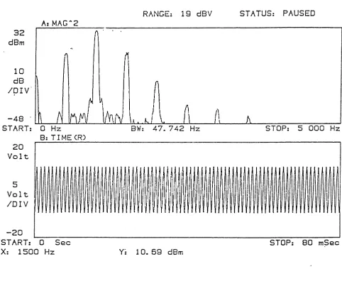
After demodulation, the baseband signal can be processed at a lower sampling rate[24-25]. At this sampling rate the time interval between samples permits extensive processing of the signal. Because of the nature of the sampling process, the lower sampling rate has to be obtained through a sampling rate transformation process called decimation.
RANGE:
19 dBV
STATUS:
PAUSED
32
dBm
.
.
.STOP: 5 000 Hz
10
dB
lorv
-48
START:
o
Hz BW: 47.742 HzB: TIME (R)
20 Volt
i
,I
~
II
~
iI
1
I
5
\
,
~
I
/1
Volt
IDlV
~
I
I
-20
START: 0 Sec
X: 1500 Hz Y: 10. 69 dBm
STOP: 80 mSec
sampling an analog signal. Therefore, Nyquist filtering is needed before sampling the signal at the desired rate. Since the original signal is already in digital form, filtering and sampling operations can be combined to allow more efficient implementations. In deciding which implementation to use, it is necessary to consider the most suitable lower sampling rate, the bandwidth of the baseband signal, hardware performance and efficiency.
5.5 All Digital Communication System
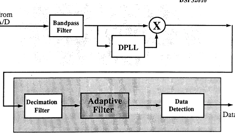
Figure 5.6 illustrates a complete all-digital receiver system(not including the AID
converter). It consists of a bandpass filter to eliminate out of band noise, a digital phase-locked loop to generate a local carrier synchronized with the carrier signal, a perfect multiplier as the demodulator, a decimation filter to lower the sampling rate,
DSP32010
- - - - -. .~~.I Bandpass
Filterf[j,
DPLLFrom
AID
an adaptive filter to separate the data signal from the harmonic noise, and a data detector. The processing tasks are divided between the DSP32010 and DSP32020, as shown in Figure 5.6.
A transmitter includes partial response coding of the data[39-40], pulse shaping, modulation, and bandpass filtering. Figure 5.7 illustrates the build blocks for a digital transmitter.
Data
~ Partial
-
Pulse----.
Coding Shaping
Bandpass
Filter ToD/A
Sinewave Generator
Figure 5.7 Digital Transmitter Implementation
Chapter 6 Summary of Achievements and Future Research
6.1 Summary of Achievements
A complete operational DSP workstation has been designed and implemented. The system has gone through extensive functional verifications by exercising all the hardware components using conventional hardware testing methods as well as run-ning various programs. The workstation features concurrent processing with two loosely coupled DSP processors to achieve ten MIPS of DSP operations. High speed communications between the two DSP processors is achieved through a dedicated data channel. A general purpose microcomputer sub-system performs major worksta-tion control funcworksta-tions. A floating point co-processor is available on the DB32016 to perform high precision computations at a relatively fast rate. The system offers 384K bytes of RAM for general purpose use and 24K bytes of RAM for DSP applications. The dual ported memory of the DSP boards allows the bus-master to perform direct-memory-access(DMA) on these memories. Non-DMA access can also take place using the Multibus I/O ports on the DSP boards. The memory configuration register on the DSP32020 allows the system to perform fast context switch during DSP pro-gram executions. A rich collection -of software development tools and DSP routines has been developed. The development tools and library routines allow the user to quickly write DSP application specific programs.
The workstation operating procedures have been established and are presented in the Workstation User Manual(see Appendix A).
6.2 Future Research
There are three major areas for future research and development. They are distri-bution line carrier communications, workstation expansion, and DSP algorithm imple-mentations.
6.2.1 DLC Implementation
The implementation of DLC systems on the workstation has just began. Specifi-cally the following areas need further development.
(1) Decimation Filter : Determine the optimal filter structure and sampling fre-quencies suitable for decimation in DLC applications. The data rate will determine the minimum sampling rate allowable. The available processing time will dictate how complex the filter can be.
(2 ) Digital Phase-Locked Loop : Define the interface between the VCO, phase detector, and lowpass filter. Given this interface, each of the functional blocks can be implemented and optimized separately for speed, performance, and efficiency. A sta-bility analysis of the digital PLL must also be performed.
(3) System Integration : Implement and test a complete transmitter/receiver sys-tem on the workstation. Plans for field testing should also be considered.
6.2.2 Workstation hardware Expansions
(1) Video Display SubSystem : A Multibus compatible video controller and dis-play terminal would further enhance the workstation's functionality. Such a subsys-tem would allow the workstation to perform real time signal analysis, displaying sig-nal waveforms and asig-nalysis results. For instance, the user could collect samples from the AID and perform an FFT for spectral analysis. Then the time domain and spectral information can be sent to the display subsystem for viewing.
(2) Mass Storage Sub-System : Eventually, the workstation can be expanded to include a mass storage subsystem for the software data base, independent of any host computer. There are variety of disk/tape controllers available for Multibus to choose from. With the addition of a storage subsystem, the user could easily collect real time signals from the field and store them for later analysis.
(3) Memory Expansion: The memory of the system could be expanded to one megabyte without using the P2 bus address lines. If a large memory space is needed on the workstation, The P2 bus must be included in address decoding. This will enable up to sixteen megabytes of memory space to be addressed in the system. Cer-tain applications may require large amounts of memory to meet speed constraints, such as in FFT operations.
(4) Next Generation DSP Processors : The new wave of DSP processors pro-vides a hope of using floating point operations instead of fixed-point arith-metic[21][29] [44-45]. These new chips, such as Texas Instruments TMS320C30 and the NEC JlPD77C25, have single cycle floating point instructions implemented in hardware. These chips open up a new array of possibilities for fast DSP algorithm
6.2.3 Additional Support Software
Additional software tools would make the workstation more powerful. These tools can be developed on the host computer.
(1) Graphic Routines : Some basic curve plotting routines are essential for the user to examine the simulation results in a graphical way. The development effort can be reduced by porting available general purpose plot routines, such as GNUPLOT.
(2) On-line Assembler/Disassembler : There are times when the user may wish to alter DSP programs after they is loaded into the DSP units' memory. To avoid re-compiling and reloading, it would be more convenient to poke the memory directly and change the code where needed. An on-line assembler/disassembler running on the workstation itself, would be a handy tool to do the job.
(3) DSP Processor Debugger: The above concept can be expanded to developing a debugger for the DSP processors, making real time DSP debugging possible.
(4) Stand-Alone Operating System : To make the workstation fully independent of any host computer assistance, a complete operating system must be developed to support the user environment. A suitable choice would be the Unix operating system.
6.2.4 DSP Algorithm Implementations
There are several subjects related to DSP algorithm implementations that would be suitable for in-depth study.
(2) Filter Tap Drift : Filter tap drift in adaptive filters, as illustrated in Figure 6.1, was observed on the workstation after the filter started normal operation for more than twenty minutes. More study needs to be conducted to gain a better understan-ding of the nature of the problem.
(3) Phase Locked-Loop : It remains a great challenge to implement a digital phase locked-loop entirely in DSP software. The performances of different types of DPLL implementations are yet to be studied.
lOdBm
-70 dBm
o
(a) Initial spectrum after filter converges
10dBm
-70 dBm
o
(b) Filter spectrum after 30 minutes
Figure 6.1 Error Signal's Spectrums of Adaptive Filter
REFERENCES
[1] A. V. Aho, J. E. Hopcroft, and J. D. Ullman, Data Structures and Algorithms,
Addison-Wesley Publishing Company, Reading, MA, 1983.
[2] M. R. Baraniecki, A. Z. Baraniecki, R. Kumaresan, and M. Shridhar,
"Multiprocessor System for Speech Processing and Telecommunications," Proceed-ings of IEEE ICASSP 84, May, 1984, pp. 25A.6.1-4.
[3] J. M. Cioffi and T. Kailath, "Fast, Recursive-Least-Squares Transversal Filters for Adaptive Filtering," IEEE Transactions on Acoustics, Speech, and Signal
Pro-cessing, Vol. ASSP-32, No.2, April, 1984, pp. 304-337.
[4] T. A. C. M. Claasen and W. F. G. Mecklenbrauker, "Adaptive Techniques for Signal Processing in Communications," IEEE Communications Magazine, Vol. 23, No. 11, Nov., 1985, pp. 8-19.
[5] L. J. Faber and T. K. Miller, "A Multiprocessor Configuration for Transversal Adaptive Filters," CCSP-WP-83/18, Dept. of Electrical and Computer Engineering, NCSU, June,1983.
[6] D. D. Falconer and L. Ljung, "Application of Fast Kalman Estimation to Adap-tive Equalization," IEEE Transactions on Communications, Vol. COM-26, Oct.,
1978,pp.1439-1446,
[7] INMOS Limited, Advance Information Data Sheet - IMS T424 Transputer, UK,
[8] J. M. McCool and Bernard Widrow, "Principles and Applications of Adaptive Filters: A Tutorial Review," IEEE Conference Paper CHI564-4/80/0000-1143, April, 1980, pp. 1143-1157.
[9] D. G. Messerschmitt, "Echo Cancellation in Speech and Data Transmission,"
IEEE Journal on Selected Areas in Communications, Vol. SAC-2, No.2, March, 1984, pp. 283-297.
[10] T. K. Miller and S. T. Alexander, "An Implementation of the LMS Adaptive Fil-ter Using an SIMD Multiprocessor Ring Architecture," Proceedings of IEEE ICASSP 85, Vol. 4, March, 1985, pp. 1605-1608.
[11] T. K. Miller and S. H. Ardalan, "A Multiprocessor Configuration for the Adap-tive Fast Kalman Algorithm," to be presented at the IEEE International Conference on Communications, June, 1986.
[12] D. P. Morgan and H. F. Silverman, "An Investigation into the Efficiency of a Parallel TMS320 Architecture: DFT and Speech Filterbank Applications," Proceed-ings of IEEE ICASSP 85, Vol. 4, March, 1985, pp. 1601-1604.
[13] L. R. Morris, Digital Signal Processing Software, DSPS Inc., Ottawa, Canada, 1983.
[14] NEC Electronics, Inc., Advanced Product Information Data Sheet - ~PD77230
Advanced Signal Processor, Feb., 1986.
[16] H. J. Siegal, "Interconnection Networks for SIMD Machines," Computer, Vol. 12, No.6, June, 1979, pp. 57-65.
[17] L. J. Siegel, "Highly Parallel Architectures and Algorithms for Speech Analysis," Proceedings of IEEE ICASSP 84, May, 1984, pp. 25A.l.1-4.
[18] Y. G. Tao, K. D. Kolwicz, C. W. K. Gritton, and D. L. Duttweiler, "A Cas-cadable VLSI Echo Canceller," IEEE Journal on Selected Areas in Communications, Vol. SAC-2, No.2, March, 1984, pp. 297-303.
[19] Texas Instruments, Inc., TMS32010 User's Guide, Dallas, TX, May, 1983.
[20] Texas Instruments, Inc., TMS32020 User's Guide, Dallas, TX, 1985.
[21] Steven L. Martin, Wave of Advances Carry DSPs to New Horizons, Computer Design, September 1987, pp. 69-83
[22] Jin-Der Wang, Analysis of Adaptive Filter Algorithms with an Application to Harmonic Noise Cancellation in Distribution Power Line Communications, Center for Communications and Signal Processing, Dept. of Electrical and Computer Engineer-ing,NCSU, August 1985
[23] R.L. Barnes, Design and Implementation of a Multiprocessor Architecture for Adaptive Digital Filters, Center for Communications and Signal Processing, Dept. of Electrical and Computer Engineering, NCSU,July 1986
[25] David J. Goodman and Michael J. Carey, Nine Digital Filters for Decimation and Interpolation, IEEE Transactions on Acoustics, Speech, and Signal Processing, vol. ASSP-25, no. 2, April 1977, pp. 121-126
[26] James C. Candy, Bruce A. Wooley, and Oconnell J. Benjamin, A voiceband Codec with Digital Filtering, IEEE Transactions on Communications, vol. COM-29, no. 6, June 1981, pp. 815-830
[27] V.B. Lawrence and A.C. Salazar, Finite Precision Design of Linear-Phase FIR Filters, American Telephone and Telegraph Company, The Bell System Technical Journal, vol. 59, no. 9, November 1980, pp. 1575-1598
[28] T.A.C.M. Claasen and W.F.G,. Mecklenbrauker, Adaptive Techniques for Signal Processing in Communications, IEEE Communications Magazine, vol. 23, no 11, November 1985, pp. 8-19
[29] John Bond, A Potpourri of DSP, The Electronic System Design Magazine, Jan-uary 1988, pp. 67-80
[30] Neal K. Riedel, David A. McAninch, Cameron Fisher, and Nahum B. Goldstein, A Signal Processing Implementation for an IBM-PC-based Workstation, IEEE Micro, October 1985, pp. 52-67
[31] F.D. Natali, Accurate Digital Detection of Angle-Modulated Signals, IEEE Elec-tronics and Aerospace Systems Convention Record, 1968, pp. 407-413
[32] Jean-Marie Blanchard, Michel Y. Levy, and Christian L. Poinas, New Algorithms for High Speed Data Receivers and Their Implementation by Microprocessors, IEEE
[33] Kamilo Feher, Ronald P. Tetare nko, Paul R. Hartmann, and Vasant K. Prabhu, Digital Communications by Radio, IEEE Transactions on Communications, vol. COM-27, no. 12, December 1979, pp. 1749-1762
[34] Raymond W. Stroh, An Experimental Microprocessor-Implemented 4800 Bitls Limited Distance Voice Band PSK Modem, IEEE Transactions on Communications, vol. COM-26, no. 5, May 1978, pp. 507-512
[35] Piet J. Van Gerwen, Niek A.M. Verhoeckx, Henk A. Van Essen, and Fred A. M. Snijders, Microprocessor Implementation of High-Speed Data Modems, IEEE Trans-actions on Communications, vol. COM-25, no. 2, February 1977, pp. 238-250
[36] Jon W. Bayless, Arthur A. Collins, and Robert D. Pedersen, The Specification and Design of Bandlimited Digital Radio Systems, IEEE Transactions on Communi-cations, vol. COM-27, no. 12, December 1979, pp. 1763-1770
[37] Friedrich JondraI, Digital Signal Processing in a Commercial Short Wave Receiv-er, Signal Processing III: Theories and Applications, Elsevier Science Publishers
B.V., North-Holland, 1986, pp. 1105-1108
[38] Norman C. Beaulieu and Cyril Leung, On the Performance of Three Suboptimum Detection Scheme for Binary Signaling, IEEE Transactions on Communications, vol.
COM-33, no. 3, March 1985, pp. 241-245
[39] Subbarayan Pasupathy, Correlative Coding: A Bandwidth-Efficient Signaling
Scheme, IEEE Communications Society Magazine, July 1977, pp. 4-11
[41] William C. Lindsey and Chak Ming Chie, A Survey of Digital Phase-Locked Loops, Proceedings of the IEEE, vol. 69, no. 4, April 1981, pp. 296-317
[42] Texas Instruments, Digital Phase-Locked Loop Design Using SN54174LS297, Dallas, Texas, 1986
[43] George Troullinos, Peter Ehlig, Raj Chirayil, Jon Bradley, and Domingo Garcia, Texas Instruments, Theory and Implementation of a Splitband Modem Using the TMS32010, 1986
[44] David Taylor, Alex Genusov, and Rami Friedlander, DSPs Finally Find Floating Point, The Electronic System Design Magazine, January 1988, pp. 81-86
[45] Bob Williams, Jim Prater, Digital Filtering: The Right Stuff/or Video, The Elec-tronic System Design Magazine, January 1988, pp. 91-94
[46] I.B. O'Neal, Overview of Power Distribution Line Carrier Communication
S)'S-tems, Conference Record IEEE Global Telecommunication Conference, pp. 464-467, November 28 - December 1 1983, San Diego, CA
[47] K.W. Whang, G.C. Cagle, and S.W. Smart, The Power Distribution System as a Communication medium for Load Management and distribution Automation, Confer-ence Record IEEE Global Telecommunication ConferConfer-ence, pp. 478-482, November 28 - December 1 1983 San Diego, CA
[48] G. Bowling, The Power Distribution System as a Communication Medium to Control of Power, Conference and Exposition, IEEE Record 79CH1377-1 Register 5, March 19-21 1979(also Rockwell International internal report)
the Power Line Carrier, Rockwell International, March 19, 1981
[50] I.B. O'Neal, Modeling the Noise on the Substation Power Distribution Bus at Frequencies from 1-20 KHz, Paper of Center for the Communications and Signal Pro-cessing, North Carolina State University, CCSP-wp-84/2, 1984
[73] R.I. Trussell, and J.D. Wang, Cancellation of Harmonic Noise in Distribution Line Communication,IEEE Transaction on Power Apparatus and Systems, to appear
[74] Brain Harry, A Macro Assembler for the TMS32010 and TMS32020 written in the C Programming Language, CCSP, North Carolina State University, 1988
[75] Todd Cook, A TMS32010132020 Simulator Written in the C Programming Lan-guage, CCSP, North Carolina State University, 1987
[76] James B. Johnson and Steve Kassel, The Multibus Design Guidebook, Structure, Architecture, and Applications, 1984
[77] National Semiconductor Corporation, Series 3200, Development Board Monitor Reference Manual, June 1984
Appaendix A Digital Communication Workstation User Manaul
TABLE OF CONTENTS
Section 1 - Introduction 60
Section 2 - System Overview 61
2.1 Hardware 62
2.2 Software 70
Section 3 - DSP Applications - An Example 71
3.1 Formulation of Application Building Blocks 72
3.2 Program Coding 72
3.3 Program Loading and Execution 74
Section 4 Run Time User-Workstation Interactions 77 4.1 Using the Debugger as a Control Tool 78
4.2 User Written Control Programs 83
Section 5 Workstation Resource Management 84
5.1 AID and D/A Converters 84
5.2 Dual Ported Memories 85
5.5 Bus Master - DB32016 85
5.6 External Memory Board 86
Section 6 Workstation's Future Expansion 86
Appendices 87
A - Multibus Data Sheet 87
B - Workstation Memory Map 88
C - DSP32010 Data Sheet 89
D - DSP32020 Data Sheet 94
E - DSP32010 to
AID
and D/A Digital Interfaces Data Sheet 105F - Program Listings 106
G - Miscellaneous Commands and Files 110
H - System Block Diagram 116
1. Introduction
The technological advance in Digital Signal Processing(DSP) has made it possible to implement communication systems in all-digital form. This is due to the fact that both the theoretical and practical aspects of the field have made tremendous progress during the past decade. As more DSP algorithms are being discovered, better tools are also being developed to implement these algorithms. One of the most important technological breakthroughs in electronics is the high-speed digital signal processor. Essentially high speed microprocessors/microcomputers and digital signal processors are designed specifically to perform computation intensive digital signal processing algorithms. These processors can execute millions of DSP operations per second by taking advantage of the advanced architecture, parallel processing, pipelining, and dedicated DSP instruction sets. These capabilities and the low cost of VLSI technology to manufacture these single-chip processors allows complicated DSP algorithms to be implemented in a tiny silicon chip with an affordable price. Digital signal processors have the advantages of reliability, reproducibility, compactness, programmability, and efficiency. The programmability makes digital signal processors very attractive for (1) system upgrades, in the case of advancements is DSP algorithms, and (2) multitasking where different tasks can be performed with the same device by simply changing its program. For the above and many other advantages, digital signal processors are being widely used in areas of general purpose digital signal processing, telecommunications, voice and speech, graphics and imaging, control, instrumentation, and the military. The purpose of the digital communication workstation is for a communication system designer and researcher to implement real time communication systems in an all-digital form by utilizing
advanced DSP technology. The workstation makes digital signal processors' attractive and powerful features easily accessible to the user by an advanced system architecture and a user friendly interface. With the workstation, communication systems can be designed and realized with minimum engineering effort. This manual is intended to give the user a good understanding of the workstation's hardware and software tools. It enables the user to utilize the workstation's available resources effectively. It also provides instructions on how to operate the workstation. The user is advised to study the references listed at the end of the manual to enhance the understanding of this manual.
The manual is organized into five sections. Section one is a brief introduction. Section two introduces the user to the workstation's hardware and describes important DSP hardware components in detail. The available software associated with the workstation's DSP applications is discussed. Section three uses a digital sinewave generator as an example to demonstrate the basic procedure of how to implement a DSP system on the workstation. Section four discusses the real-time interaction between the user and the workstation. Section five looks at each of the workstation's hardware components and examines the ways to manage these resources.
2. System Overview
The following sections describe in detail the hardware construction of the workstation and introduces the software tools available to operate the workstation efficiently. The system block diagrams shown in Appendix H of this manual will enhance understanding of this section.
2.1 Hardware Description
The architecture of the workstation is best described as a multicomputing configuration. It uses a Multibus I interface as the system bus. There are presently three processing units (boards) on the bus. Each of three boards has a microprocessor, local
I/O
channels, and shared-local memory. The fourth board is a memory expansion board. The National Semiconductor Corporation DB32016 single board computer serves as the bus master and performs system control functions of the workstation. Two Digital Signal Processing boards are built around Texas Instrument's TMS320 DSP family single-chip microcomputers. These two boards arededicated to perform actual digital signal processing, operating at 20MHz. A Plessey PSM512A Multibus Error-Correction DRAM board has been installed to expand the system memory capacity by 256Kbytes.
2.1.1 System Bus - Multibus Interface
The Multibus system bus was originally developed at Intel Corporation in 1975 and later evolved to become the IEEE Standard 796-1983. Often referred to as MultibusIIEEE-796, it is a commercial-quality industry-standard open architecture bus for the use in microprocessor-based systems. The bus supports independent memory and I/O address spaces. There are 16 megabytes directly addressable memory and 64K I/O ports. Devices with either 8-bit or 16-bit(or both) data path(s) can transfer data over the bus using the asynchronous bus cycle protocol. The master-slave bus structure concept allows devices of different speeds to be interfaced via the bus handshaking mechanism. Data transfer rates up to five million transfers(bytes or words) per second are conceivable.
The Multibus interfacing system also provides three subsidiary busses in addition
to the system bus. They are the iSBX bus, iLBX bus, and MULTICHANNEL bus. However, they are not implemented in the workstation design because of the cost and complexity considerations. Instead, a dedicated I/O channel interface, P2 Data Channel, is introduced in place of the iLBX bus to enhance the performance of the digital signal processing units. It is configured using the form-factor of a standard 60-pin Multibus P2 connector. The signal definitions are described in Appendix A of this manual. The bus backplane is a MUPAC Multibus cage with five PI bus slots.
2.1.2 Bus Master - DB32016 Single Board Computer
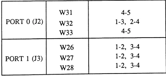
The DB32016 single board computer is a complete microcomputer using the National Semiconductor Series 32000 family of advanced microprocessors. It is equipped with an EPROM-based firmware, MON16 monitor, which provides a native debug and execution environment for programs developed on a host computer. The National's C cross software package, residing on a Micro-VAX II, provides a high level programming environment for the user to develop software for the DB32016. The Multibus interface permits the DB32016 microcomputer system to be used on the industry standard Multibus system bus as the bus master for the workstation. The board includes a NS32016 CPU, a NS32082 Memory Management Unit(MMU), a NS32081 Floating-Point Unit(FPU), and a NS32202 Interrupt Control Unit(ICU). The 128 Kbytes of on-board dynamic RAM is configured as local memory to the DB32016 board. A PROM-based fmnware MON16 monitor, which resides on two 2732 PROMs with a 450 ns access time, is installed on the DB32016 board. The jumper setting requirements are shown in Table 1.
TABLE 1 JUMPER SETIING FOR PROM INSTALLATION
Two serial I/O ports are provided via an 8251A USART(Universal Synchronous
W6 9-10
Wl1 1-2, 5-6
W3 3-4, 7-8
Asynchronous Receiver Transmitter). These ports establish the user-to-workstation-to-host-computer interface through two RS232 connections(DTE and
DeE) configured in transparent mode. A standard terminal-display with a keyboard is connected to serial port 0, designated as J2, while serial port 1, designated as J3, is connected to a Micro-VAX IT as the host computer. Both ports are operating at a 9600 baud speed. The jumper settings are listed in Table 2.
TABLE 2 JUMPER SETIING FOR PORT 0 AND PORT 1
W31 4-5
PORT 0 (J2) W32 1-3, 2-4
W33 4-5
W26 1-2, 3-4
PORT 1 (J3) W27 1-2, 3-4
W28 1-2, 3-4
Port 0 is configured as a DCE(data communication equipment) with handshaking and port 1 is configured as a DTE(data terminal equipment) without handshaking. The dip switch S3 is set as follows: position 4 closed, position 3 closed, position 2