University of Windsor University of Windsor
Scholarship at UWindsor
Scholarship at UWindsor
Electronic Theses and Dissertations Theses, Dissertations, and Major Papers
10-5-2017
Design for Test and Hardware Security Utilizing Tester
Design for Test and Hardware Security Utilizing Tester
Authentication Techniques
Authentication Techniques
Yahia OUAHAB University of Windsor
Follow this and additional works at: https://scholar.uwindsor.ca/etd
Recommended Citation Recommended Citation
OUAHAB, Yahia, "Design for Test and Hardware Security Utilizing Tester Authentication Techniques" (2017). Electronic Theses and Dissertations. 7286.
https://scholar.uwindsor.ca/etd/7286
This online database contains the full-text of PhD dissertations and Masters’ theses of University of Windsor students from 1954 forward. These documents are made available for personal study and research purposes only, in accordance with the Canadian Copyright Act and the Creative Commons license—CC BY-NC-ND (Attribution, Non-Commercial, No Derivative Works). Under this license, works must always be attributed to the copyright holder (original author), cannot be used for any commercial purposes, and may not be altered. Any other use would require the permission of the copyright holder. Students may inquire about withdrawing their dissertation and/or thesis from this database. For additional inquiries, please contact the repository administrator via email
Design for Test and Hardware Security Utilizing Tester Authentication Techniques
By
Yahia OUAHAB
A Thesis
Submitted to the Faculty of Graduate Studies
through the Department of Electrical and Computer Engineering in Partial Fulfillment of the Requirements for
the Degree of Master of Applied Science at the University of Windsor
Windsor, Ontario, Canada
2017
Design for Test and Hardware Security Utilizing Tester Authentication Techniques
Yahia OUAHAB
APPROVED BY:
______________________________________________ E. Tam
Mechanical, Automotive & Materials Engineering
______________________________________________ E. Abdel-Raheem
Electrical and Computer Engineering
______________________________________________ R. Muscedere, Co-advisor
Electrical and Computer Engineering
______________________________________________ R. Rashidzadeh, Advisor
Electrical and Computer Engineering
iii
DECLARATION OF CO-AUTHORSHIP / PREVIOUS PUBLICATION
I. Co-Authorship
I am aware of the University of Windsor Senate Policy on Authorship and I certify that I have properly acknowledged the contribution of other researchers to my thesis, and have obtained written permission from each of the co-author(s) to include the above material(s) in my thesis.
I certify that this thesis and the research to which it refers, is the product of my own research study guided by my supervisor and co-supervisor.
II. Previous Publication
This thesis includes three original papers that have been previously published/submitted for publication in peer reviewed journals, as follows:
Chapter Publication Title Publication Status Chapter -3 Y. Ouahab, D. Richard, R. Rashidzadeh,
“Secure scan chain using test port for tester authentication,” 23rd IEEE International Conference on Electronics, Circuits and Systems (ICECS), Monte Carlo, Monaco, December 2016.
Accepted
Chapter-4 Y. Ouahab, R. Rashidzadeh, R. Muscedere, “A Secure Scan Chain Using a Phase Locking System and a Reconfigurable LFSR,” IEEE 30th Canadian Conference on Electrical and Computer Engineering (CCECE), Windsor, On, Canada April 2017.
Accepted
Chapter-5 Y. Ouahab, R. Rashidzadeh, R. Muscedere, “Effect of Wafer Thinning on Hardware Security,” IEEE the 50th International Symposium of Circuits and Systems (ISCAS), Florence, Italy May 2018.
iv
I certify that I have obtained a written permission from the copyright owner(s) to include the above published material(s) in my thesis. I certify that the above material describes work completed during my registration as a graduate student at the University of Windsor.
III. General
I declare that, to the best of my knowledge, my thesis does not infringe upon anyone’s copyright nor violate any proprietary rights and that any ideas, techniques, quotations, or any other material from the work of other people included in my thesis, published or otherwise, are fully acknowledged in accordance with the standard
referencing practices. Furthermore, to the extent that I have included copyrighted material that surpasses the bounds of fair dealing within the meaning of the Canada Copyright Act, I certify that I have obtained a written permission from the copyright owner(s) to include such material(s) in my thesis.
v
ABSTRACT
Design-for-Test (DFT) techniques have been developed to improve testability of
integrated circuits. Among the known DFT techniques, scan-based testing is
considered an efficient solution for digital circuits. However, scan architecture can
be exploited to launch a side channel attack. Scan chains can be used to access a
cryptographic core inside a system-on-chip to extract critical information such as a
private encryption key. For a scan enabled chip, if an attacker is given unlimited
access to apply all sorts of inputs to the Circuit-Under-Test (CUT) and observe the
outputs, the probability of gaining access to critical information increases. In this
thesis, solutions are presented to improve hardware security and protect them against
attacks using scan architecture. A solution based on tester authentication is presented
in which, the CUT requests the tester to provide a secret code for authentication. The
tester authentication circuit limits the access to the scan architecture to known
testers. Moreover, in the proposed solution the number of attempts to apply test
vectors and observe the results through the scan architecture is limited to make
brute-force attacks practically impossible. A tester authentication utilizing a Phase
Locked Loop (PLL) to encrypt the operating frequency of both DUT/Tester has also
been presented. In this method, the access to the critical security circuits such as
crypto-cores are not granted in the test mode. Instead, a built-in self-test method is
used in the test mode to protect the circuit against scan-based attacks. Security for
new generation of three-dimensional (3D) integrated circuits has been investigated
through 3D simulations COMSOL Multiphysics environment. It is shown that the
process of wafer thinning for 3D stacked IC integration reduces the leakage current
vi
DEDICATION
I would like to thank my Lord at first for this achievement, my wonderful family –
parents, groupmate and friends for their helping hand and encouragement from
close or far.
Special thanks for my supervisor, Dr. Rashid Rashidzadeh, for his guidance and
vii
ACKNOWLEDGEMENTS
I deeply appreciate my supervisor Dr. Rashid Rashidzadeh for his exceptional
guidance and support. He provided me with excellent financial and technical
supports to conduct my research in a great research oriented environment.
I would also like to thank my co-supervisor Dr. Roberto Muscedere for his
appreciated explanations and feedback.
Special thanks to my honorable committee members including Dr. Esam
Abdel-Raheem, Dr. Edwin Tam for their time and valuable comments on my research
studies.
I would like to thank my fellow laboratory members as well at the Research Centre
viii
TABLE OF CONTENTS
ABSTRACT ... v
DEDICATION ... vi
ACKNOWLEDGEMENTS ... vii
LIST OF TABLES ... xi
LIST OF FIGURES ... xii
LIST OF ABBREVIATIONS/SYMBOLS ... xiv
Chapter -1... 1
Background & Introduction ... 1
1.1 Very Large Scale Integration (VLSI)... 1
1.2 Why Testing ICs ... 1
1.3 Testing ICs ... 3
1.4 Challenges in testing ICs [11-13 I]: ... 4
1.5 Categories of Testing Digital Circuits ... 5
1.6 Three Dimensional Integration Circuits 3D (ICs) ... 5
1.7 Research Objectives ... 8
1.8 Thesis contributions ... 8
1.9 Thesis Overview ... 9
1.10 References ... 10
Chapter -2... 11
Design for Testability ... 11
2.1 DFT ... 11
2.2 AD hoc ... 11
2.3 Built-in self-test (BIST): ... 12
2.4 Scan Based Test ... 13
2.5 References ... 15
Chapter -3... 16
ix
3.1 Introduction ... 16
3.1.1 Related Works ... 16
3.1.2 Class of attackers ... 17
3.2 Proposed Tester Authentication Based Security Measure Against Scan Based Attack ... 18
3.2.1 Tester Authentication Block ... 18
3.2.2 Scan based attacks ... 20
3.2.3 Secure Scan Chain ... 21
3.2.4 Implementation ... 22
3.2.5 Comparative Analysis ... 24
3.3 Conclusion ... 25
3.4 References ... 26
Chapter -4... 28
A Secure Scan Chain Using a Phase Locking System and a Reconfigurable LFSR ... 28
4.1 Introduction ... 28
4.1.1 Related works ... 28
4.1.2 The proposed method ... 29
4.1.3 Paper’s organization ... 30
4.2 Device Authentication Security Measure ... 30
4.2.1 Synthesizer ... 31
4.2.3 Tester Authentication sequences ... 32
4.3 The Proposed Secure Scan Chain Architecture ... 33
4.4 Implementation ... 35
4.4.1 Area Overhead ... 35
4.5 Conclusion ... 37
4.6 References ... 38
Chapter-5... 40
Effect of Wafer Thinning on Hardware Security ... 40
5.1 Introduction ... 40
5.1.1 Related Works ... 40
5.1.2 Contributions... 41
5.2 Model Definition and Parameters ... 42
5.2.1 (3D) Model Structure ... 42
x
5.3 Results and Discussion ... 47
5.3.1 Performance Analysis ... 47
5.3.2 Security Analysis ... 51
5.4 Conclusion ... 53
5.5 References ... 54
Chapter -6... 56
Conclusions and future works ... 56
6.1 Conclusions ... 56
6.2 Future Works ... 57
Appendix: Copyright permission ... 56
xi
LIST OF TABLES
Table I: AREA OVERHEAD MESUREMENTS……..…………...………..25
Table II: GATE AREA OVERHEAD MESUREMENTS………..36
Table III: VALUES PARAMETERS USED IN THE DESIGN OF N-MOSFET.44
Table IV: LEAKAGE CURRENT DEPENDENCE ON WAFER THICKNESS
xii
LIST OF FIGURES
Figure -1 A wafer combining more than millions of transistors (VLSI design)...1
Figure- 2 Different process steps involved in the fabrication VLSI components.2 Figure -3 Cost (cents/transistor) evolution fabrication and effort for testing……3
Figure- 4 Testing of digital integrated circuits………..4
Figure- 5 Six levels copper metal interconnects of CMOS chip developed by IBM………4
Figure- (a) 3D IC integration using Through Silicon Vias (TSV) and (b) 16Gb NAND flash stack using TSV developed by Samsung……….6
Figure- 7 interconnections of DRAM to a logic. (a) Planar technology. (b) System on Chip (SOC). (c) 3D stacked Si wafer………...7
Figure- 8 Ad hoc test using test point insertion………...12
Figure- 9 Built-In Self-Test (BIST) based DFT testing………...12
Figure- 10 Converting a sequential circuit into scan design. (a) Combinational logic with ordinary flip-flop. (b) Scan design………..13
Figure- 11 Symbol of Scan Flip-flop (SFF)……….…13
Figure -12 A typical example of a scan chain……….14
Figure- 13 Tester authentication block diagram………...18
Figure -14 Two phases of test port for authentication……….….19
Figure 15. Tester Authentication Block constitution………....20
Figure 16 Hardwired flip-flops with BIST to store encryption key………….…22
Figure- 17 Area overhead of the authentication block……….…23
Figure- 18 Two phases of test port for authentication Sequences………....30
Figure- 19 Block diagram of (a) a Conventional PLL and (b) a PLL based Synthesizer………...31
Figure -20 Tester Authentication Module………....32
Figure-21 Proposed architecture of N-bit secret key at the safe mode……….…33
xiii
Figure -23 Area overhead of the proposed solution using TSMC 65nm CMOS
technology………...35
Figure -24 Schematic diagram of a typical MOSFET……….42
Figure- 25 Volume plot of initial modeled doping………..43
Figure-26 Volume plot showing the total net dopant concentration of MOSFET.43
Figure-27 Simulation results for I-V characteristics for both 45/22 [nm]
n-MOSFET; (a)-(b) ID versus VG for VD=VDD normal and logarithmic scale
respectively……….…….45
Figure- 28 Simulation results for I-V characteristics for both 45/22 [nm]
n-MOSFET; (a)-(b) ID versus VD for VG=0.9 -1.2 V respectively…………..….46
Figure- 29 ID–VD characteristics comparison as function of the Si body thickness
(H) from 400 to 6[nm] for n-MOSFET 45[nm] at medium VG voltage (0.9
V)………...…..…47
Figure -30 ID–VD characteristics comparison as function of the Si body thickness
(H) from 400 to 6 [nm] for n-MOSFET 45 [nm] at high VG voltage (1.2 V)…..48
Figure- 31 ID–VD characteristics comparison as function of the Si body thickness
(H) from 400 to 6 [nm] for n-MOSFET 22 [nm] at medium VG voltage (0.9V)...48
Figure- 32 ID–VD characteristics comparison as function of the Si body thickness
(H) from 400 to 6 [nm] for n-MOSFET 22 [nm] at high VG voltage (1.2 V)……49
Figure- 33 ID–VD characteristics comparison as function of the Si body thickness
(H) from 400 to 6 [nm] for n-MOSFET 45 [nm] at high VG voltage (1.2 V)……49
Figure- 34 ID–VD characteristics comparison as function of the Si body thickness
(H) from 400 to 6 [nm] for n-MOSFET 45 [nm] at high VG voltage (1.2 V)...50
Figure -35 ID–VD characteristics comparison as function of the Si body thickness
(H) from 400 to 6 [nm] for n-MOSFET 22 [nm] at high VG voltage (1.2 V)……50
Figure- 36 ID–VD characteristics comparison as function of the Si body thickness
(H) from 400 to 6 [nm] for n-MOSFET 22 [nm] at high VG voltage (1.2 V)……51
Figure- 37 Commonly accepted leakage currents dependence based on input
patterns of four terminals n-MOSFET on input patterns………..51
Figure- 38 (a)-(b) Leackage Current Ioff (uA) Vs Si thickness for n-MOSFET 45
xiv
LIST OF ABBREVIATIONS/SYMBOLS
ABBREVIATIONS DESCRIPTION
AC/DC ATPG BIST CFSR CUT DFT DUT ICs Ioff Ion IPs JTAG LDPA LFSR LPA LSI MISR MOSFET MSI SFF SISR SOC SSI TAM TAP TAPC TCK TDI
Alternating/ Direct Current
Automatic Test Patterns Generator
Built-in Self-Test
Complete LFSR
Circuit Under Test
Design for Testability
Device Under Test
Integrated Circuits
Leakage Current
On Current
Intellectual Properties
Joint Test Action Group
Leakage Differential Power Analysis
Linear Feedback Shift Register
Leakage Power Analysis
Large Scale Integration
Multiple Input Shift Register
Meatal Oxide Semiconductor Field Effect Transistor
Medium Scale
Scan Flip-Flop
Single Input Shift Register
System On Chip
Small Scale Integration
Test Access Mechanism
Test Access Port
Test Access Port Controller
Test Clock
xv
TDO
TMS
TRST
TSV
VLSI
3D ICs
Test Data Output
Test Mode Select
Test Reset
Through Silicon Via
Very Large Scale Integration
1
Chapter -1
Background & Introduction
1.1 Very Large Scale Integration (VLSI)
Very large scale integration (VLSI) has been introduced in the early 1980s, with the
integration of millions of transistors on one die Fig. 1. As a result, manufacturing tests for
such a high density integrated circuit became a major problem to solve. Test engineers
faced various challenges on how to perform manufacturing tests as VLSI technology
evolved [1].
1.2 Why Testing ICs
The steady increase in the number of transistors within a single chip resulted in the
progression from small scale to very large sale. Most current VLSI design systems such as,
smartphones, workstations and various electronic appliances, incorporate hundreds of
millions of transistors. The reduction of feature sizes of transistors to sub-micron and the
interconnect wires to tens of nanometers have increased the density of transistors per chip
significantly.
2
The small feature sizes resulted in a substantial increase in the operating frequency of
integrated circuits [1]. However, shrinking feature sizes and increasing the number of
transistor on a single chip can increase the chance of defects. Considering sub-nanometer
technology, defects may occur in manufacturing process that can lead to a faulty transistor
or an interconnect wire. Manufacturing defects of ICs are inevitable as it requires a single
transistor or interconnect to break down the functionality of the entire chip or at least
prevent the system from proper operation at the desired frequency. There is factor known
as Part Per Million (PPM) which indicate the quality of the ICs launched to the market.
PPM indicates how many ICs out of one million are faulty. In general, a PPM of 50 is
considered acceptable for commercial applications. For certain applications such as
military projects, this rate much lower and falls below 4 PPM. Thus, it is highly required
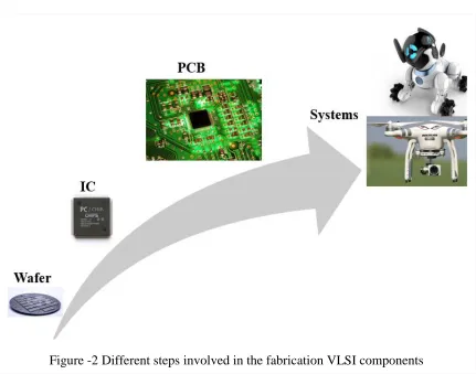
to test VLSI devices at different stages of device production Fig. 2.
Testing ICs can potentially increase the production yield [3]. Enhancing the yield can occur
3
methods of testing integrated circuits are required to reduce the overall costs of IC
fabrication prior to releasing them to the market [4].
According to Fig. 3 from Advanced Reliable System (ARES) Lab, the costs of testing per
transistor has increased over the last two decades while the fabrication costs per transistor
has declined [5].
1.3 Testing ICs
Testing digital circuits is usually performed based on the needs of consumers and design
specifications using an Automatic Test Pattern Generator (ATPG) to generate test patterns
[6]. In certain cases, Built-in Self-test (BIST) methods are used to generate the test stimuli
to test a device without external equipment [4].
In the test phase, the test stimuli are applied to the circuit under test (CUT) as shown in
Fig. 4. The output responses are then captured and compared against the expected outputs
to determine fault-free and faulty ICs. A circuit-under-test has to produce desired output
4
1.4 Challenges in testing ICs [11-13 I]:
Fig. 5 presents a physical illustration of a short channel Silicon on Insulator (SOI)
fabrication technology with six levels of metals for interconnections. A typical chip in this
technology can include more than 60 miles (100 kilometers) of copper wiring. Process
variations can affect directly the internal characteristics of the fabricated transistor such us,
threshold voltage and transit frequency. The introduction of nanometer technology has
increased the probability of parametric and catastrophic failure during ICs fabrication
which is considerably high compared to the traditional CMOS technology. Sub-nanometer
technology is characterized by high sensitivity to noise due to the lower current that can be
delivered [8-10]
Figure- 4 Testing of digital integrated circuits [7]
Input
Test
Stimuli
Circuit
Under Test
(CUT)
Output
Response
Analysis
Pass/Fail
Input
1Input
nOutput
1Output
n5
1.5 Categories of Testing Digital Circuits
Testing of digital circuits is divided into three categories of (a) functional, (b) structural
and (c) parametric tests. Testing integrated circuits starts with wafer level testing to mainly
determine catastrophic faults and sort wafers.
Once wafers are successfully passed the test, one of the three methods can be chosen to
perform tests as illustrated in Fig. 4 [4].
1. Functional test: as its name indicates used to check the functionality of the design.
In this method, the test stimuli are chosen based on the functionality of the CUT. A
set of test stimuli are applied to the CUT, and the responses are compared against
the expected outputs. This method of testing can be very time consuming for
modern integrated circuit and the fault coverage can be limited.
2. Structural test: this is a time efficient method of testing. In this approach, fault
models are considered to generate test patterns regardless of the functionality of the
CUT.
3. Parametric test: this method of testing, AC and DC parametric tests can be
performed mainly on analog circuits. The DC parametric tests are commonly
conducted to determine open paths, short paths, threshold voltage and leakage
current. The AC parametric testing focuses more on the AC parameters such as,
frequency, timing, noise, distortion and bandwidth. This approach relies on
dedicated instrument (built-in digital signal processing) to perform testing.
1.6 Three Dimensional Integration Circuits 3D (ICs)
Three-dimensional (3D) integration refers to the integration of multiple layers of planar
devices on a single chip. In such an architecture, the layers are stacked upon each other and
6
There are several manufacturing steps to design such an architecture including, TSV
formation, wafer thinning, alignment and bonding [13].
(a)
(b)
7
3D stacked IC integration can reduce the interconnect delay significantly taking advantage
of the vertical interconnect using (TSV). In 3D ICs, each layer is commonly assigned to a
specific application. For example, the integration of CPUs, SRAM, logic IC, power and
analog modules are designed on different layers. Fig. 7 presents the interconnections of
embedded DRAM to a logic circuit using three different technologies.
The current (2D) scheme is a platform where layers are connected horizontally using long
wires as shown in Fig. 7 a. System-on-chip (SOC) scheme Fig. 7b incorporates all aspects
of system design on a single die. However, it has a negative impact on the silicon area and
increases the length of interconnection wires, which in turn increases the path delays.
Besides, (SOC) requires a higher material complexity to assemble different technologies
in one chip. 3D integration technology can reduce the length of interconnect wires which
results in lower power consumption, higher speed of operation and smaller form factor
compared to the SOC technology. 3D stacked ICs include various layers on top of each
other. Each layer is thinned down and aligned to another layer to form multiple layers with
the same size as shown in Fig. 7c. As a result, a 3D integration scheme offers a higher
performance and functionality compared to the traditional technologies (2D) and SOC as
it permits integration of different technologies [14].
Figure- 7 Connecting DRAM to a logic. (a) Planar technology. (b) System on Chip (SOC). (c) 3D stacked IC [13]
8
1.7 Research Objectives
One of the most power DFT techniques for digital circuit is the scan-based testing method
which can increase the controllability and observability considerably. However, increasing
the controllability and observability through scan architecture provides opportunities to
attackers to use the scan architecture to access critical information such as a private key of
an embedded crypto-core. Moreover, the scaling of transistors to a few nano-meter
increases the leakage current considerably which can also be used to obtain critical
information by hardware attacker.
The objective of this research is to use a tester authentication technique to design a secure
scan architecture. Moreover, the effect of wafer thinning on the security of 3D ICs will be
investigated. The major focus is on designing area and cost efficient hardware solutions to
protect the scan chain from side channel attacks. There is a dependency between the
leakage current of a digital circuit on the status of its inputs. The switching of a digital gate
from high to low level or vice versa affects the leakage current. Considering this
correlation, an attacker can perform static power analysis on digital circuits to extract
critical information. The process of wafer thinning reduce the leakage current and lowers
the probability of a successful attacks by adversaries.
1.8 Thesis contributions
The research contributions of this thesis are summarized as follows which have been
presented in three conference papers:
1. A security solution against scan based attacks using a tester authentication
technique has been developed. Unlike previously proposed methods where tester
has unlimited access to the CUT, in this method after a certain number of trails the
access is denied. The circuit under test (CUT) communicates with the tester
requesting an identification key before allowing the tester to access the scan chain.
2. A new security solution using a phase locking loop system (PLL) to obfuscate the
9
3. The effect of wafer thinning on security of 3D integrated circuits has also been
studied. The results indicates that wafer thinning lowers the static power
consumption improves the chip security.
1.9 Thesis Overview
This thesis is organized as follows:
Chapter-1 Introduction and background, which provides a brief description of current VLSI
systems, testing and challenges of testing these devices.
Chapter -2 introduces three main Design for Testability techniques. Also, it provides details
of “Scan Architecture” and hardware security threats due to scan chains.
Chapter-3 presents the first published paper entitled” Secure Scan Chain using Test Port
for Tester Authentication” in which a tester authentication technique has been presented.
In this approach, access to the scan chain is restricted to only certified testers using a secret
key in which the number of attempts is limited.
Chapter-4 presents the second published paper entitled” A Secure Scan Chain using a PLL
and a Reconfigurable LFSR” in which two layers of security have been added to protect
scan chain from side channel attacks. A tester authentication method based on a Phase
Locked Loop (PLL) system to obfuscate the clock frequency, and a Built-In Self-Test
(BIST) method using internal structure to generate the test patterns are presented.
Chapter-5 presents the third paper entitled” Effect of Wafer Thinning on Hardware
Security” in which COMSOL Multiphysics has been used to model two transistors with
gate length of 45nm and 22 nm in order to evaluate and analyze the effect of wafer thinning
on chip security.
In this chapter, it is shown that wafer thinning process improves the chip security against
leakage-based differential power analysis (LDPA) threats.
10
1.10 References
[1] Gordon E. Moore, “Cramming more components onto integrated circuits”, Electronics, Vol 38, no 8, pp. 114–117, 1998.
[2] Anand Lal Shimpi. Marc Prieur. A Quick Look at a 22nm Ivy Bridge Wafer. May 31, 2011.
[3] N. K. Jha and S. K. Gupta,”Testing of Digital Systems”, Cambridge University Press, Cambridge, U.K., 2003.
[4] F. Saqib, & J. Plusquellic. VLSI Test and Hardware Security Background for Hardware Obfuscation. In Hardware Protection through Obfuscation (pp. 33-68). Springer International Publishing. (2017)
[5] Jin-Fu Li. VLSI Testing. Chapter 6. Advanced Reliable Systems (ARES) Laboratory Department of Electrical Engineering National Central University Jungli, Taiwan.
[6] A.K. Stevens, Introduction to computer Testing, Reading Massachusetts: Addision- Wesley, 1986.
[7]L.-T. Wang C.-W. Wu X. Wen, “VLSI Test Principles and Architectures: Design for Testability,” 2006.
[8] C. E. Stroud, A Designer’s Guide to Built-in Self-Test, Kluwer Academic, Norwell, MA, 2002.
[9] C. Stroud, J. Emmert and J. Batley, A new bridging fault model for more accurate fault behavior, in Pro Automatic Test Conference (AUTOTESTCON), pp. 481-485, September 2000.
[10] A.J Van de Goor, Testing Semiconductor Memorises: Therory and Practise, Jhon Wiley and Sons, Chichester, U.K. 1991.
[11] L. Geppert, Technology 1998 Analysis and forecast: IEEE Solid State Spectrum, Vol 35, no 1, pp. 23-28, 1998.
[12] M. Jung, J. Mitra, D. Z. Pan, & S. K. Lim,” TSV stress-aware full-chip mechanical reliability analysis and optimization for 3D IC”, Communications of the ACM, 57(1), 107-115. (2014).
[13] S. J. Koester, A. M. Young, R. R. Yu, S. Purushothaman, K. N. Chen, D. C. La Tulipe, ... & E. J. Sprogis. Wafer-level 3D integration technology. IBM Journal of Research and Development, 52(6), 583-597. (2008).
11
Chapter -2
Design for Testability
In the past, designing and testing integrated circuits were considered two separate issues,
handled by different groups of engineers. During that time, design engineers used to focus
more on how to meet the prerequisite functionally rather than the testability of the circuits.
Test engineers had to develop time and cost effective methods to test the designed ICs.
With this method, manufacturers achieved high fault coverage for small-scale integrated
circuits. The weakness of this method became apparent with the introduction of VLSI
systems due to the complexity of VLSI designs.
Designing VLSI systems without test consideration increases the design complexity and
the time required for testing. Modern circuit designs are developed based on the
design-for-testability (DFT) methods. Currently chip designers have access to powerful CAD tools
developed based on efficient DFT techniques. This CAD tools can be readily used to ensure
the testability of circuits and desired fault coverage [1].
2.1 DFT
Design-for-Test (DFT) techniques have been developed to improve testability and reduce
the costs of testing integrated circuits [2]. DFT techniques help test engineers to save time
and effort to develop test solutions for integrated circuits. DFT techniques can reduce the
complexity of testing sequential circuits to a degree where the testing a sequential circuit
becomes similar to that of a combinational logic. The main DFT methods are (a) Ad hoc,
Built-in self-test (BIST) and scan based testing [1].
2.2 AD hoc
Ad hoc is considered a DFT technique dedicated to improving the testability of circuit parts
that are unreachable directly. The basic principle of Ad hoc is to add extra circuitry to the
original circuit to provide access to the internal nodes using Test Point Insertion. An
example is illustrated in Fig. 8 where a 2-to-1 multiplexer has been added as a test point to
12
2.3 Built-in self-test (BIST):
Built-in self-test is developed to perform an autonomous system testing where test patterns
are internally generated without the need to any external device such as an ATPG [3]. BIST
integrates a test-pattern generator (TPG) at its input and an output response analyzer (ORA)
at its output to apply test vectors internally to the ICs and analyze the output responses
respectively as illustrated in Fig. 9.
Figure- 8 Ad hoc test using test point insertion [1]
13
2.4 Scan Based Test
Scan based test methodology is considered as one of the most important and efficient DFT
techniques. Using a scan-based test method, sequential circuits are converted to a
combination of flip-flop chains and combinational logics as shown in Fig 10 a.
Besides, each traditional flip-flop is converted to a scan flip-flop (SFF) as indicated in Fig.
11. A scannable flip-flop has two distinct inputs sources to be selected through a 2-to-1
multiplexer as shown in Fig. 10b. The flip-flops are connected properly together to create
a shift register called scan chain.
(a) (b)
Figure- 10 Converting a sequential circuit into scan design. (a) Combinational logic with ordinary flip-flop. (b) Scan design [1]
14
The Mux used in SFF permits the scan cell to operate in two different modes:
1. Normal/ Capture mode: in this mode, the scan cell operates as a conventional
flip-flop where the first input (DI) is selected to update the output.
2. Shift mode: in this mode it is possible to insert test patterns to all scan cell in the
scan chain through one or more primary inputs. Also, the content of scan cells
supplied by the combinational logic of circuit can be shifted out through one or
more primary output as depicted in Fig. 12
Scan architecture provides direct access into the internal nodes of modern VLSI designs
including crypto-chips that could be unreachable without the scan architecture.
Although scan based test techniques have been widely adopted for modern circuit
testing, it can open a back door for hackers to perform side channel attacks and retrieve
secure information. Therefore, novel techniques to protect ICs in the test mode are
required to fulfill the requirements of both testability and security [4].
15
2.5 References
[1] L.-T. Wang C.-W. Wu X. Wen, “VLSI Test Principles and Architectures: Design for Testability,” 2006. [2] J. Aerts, & E. J. Marinissen, “Scan chain design for test time reduction in core-based ICs," Test Conference, 1998. Proceedings, International. IEEE, 1998.
[3] F. Saqib, & J. Plusquellic. VLSI Test and Hardware Security Background for Hardware Obfuscation. In Hardware Protection through Obfuscation (pp. 33-68). Springer International Publishing. (2017).
16
Chapter -3
Secure Scan Chain using Test Port for Tester Authentication
3.1 Introduction
Test engineers seek for greater controllability and observability in order to manage test
stimuli and observe the responses. Scan architecture is known as an effective DFT measure
for digital circuits. Scan chains are used to increase the testability of circuits to apply test
vectors and observe their responses. However scan architecture can also be used as a back
door for hackers to break down a chip security [2]. Scan architecture has been used to hack
various crypto hardware implementations such us AES, RSA etc. A secure scan
architecture to protect CUT against scan-based attacks while maintaining a high
controllability and observability has become a design requirement. There are two
commonly used methods to provide security for scan architecture against potential attacks.
First, the access to the scan chain is restricted using a private controller. Second, the access
to the scan chain is open; however, the data are encrypted [3].
3.1.1 Related Works
Many solutions to protect crypto cores against the scan chain attacks have been reported in
the literature. In [4] access to the scan chain is granted only if a predetermined key is
entered. Test patterns are used as the authentication keys to allow access to the scan chain
[5]. A function/test mode control method has been proposed in [6]. It limits the transitions
between normal function mode and the test mode for crypto cores. However, this method
is not suitable for at-speed online testing.
The second secure scan architecture method allows access to the scan chain but during the
scan-out phase, the data is encrypted. In this method, the scan structure is modified using
different methods such as adding gates like invertor, XORs, XNORs or scrambling the scan
chain. Various encryption methods are used to encrypt the actual scanned output and make
the output data as random as possible so that the attacker is unable to deduce the secret
17
scan technique [7]. In this technique, inverters are randomly placed in the scan chain to
confuse the attacker, as the locations of the invertors in the scan chain are not known to the
attacker. Although, it is difficult to guess the location of the invertors but a “reset” attack
on the system can reveal the location of the invertors. When the flip flops are reset, the
scan out become a stream of zeroes with ones indicating the locations of invertors.
Another secure scan architecture is the random placement of XORs between scan cells [8].
This serves to confuse attacker as the nature of the gates inserted would be unclear and the
attacker might not consider the possibility. This method offers better security than the
above technique since this method passes the “reset” attack. Most of the available solution
for a secure scan architecture allow the testers to access the scan chain, apply test vectors
and observe the output responses. Moreover, the access to the scan chain is not limited and
tests can be performed any number of times. Therefore, there is a possibility of access to
critical information through analysis of applied inputs and corresponding outputs.
3.1.2 Class of attackers
Depending on the required level of security and the possible class of attackers, different
measures can be taken. The solutions range from a basic security solution to a full fledge
encryption method. An attacker can be categorized as follows [4]:
1. Beginners: As the name indicates, someone who is new in the field.
Independents: The hackers of this class are experienced. An independent attacker has large
resources, a good knowledge of the field and can easily hack basic security systems.
2. Business: Hackers in this class are performing business secret activities. They
commonly work in organized groups with highly qualified attackers. They have
access to sophisticated hardware and software packages to wage attacks. These
activities are commonly supported by governments trying to access security
information. If we consider a novice hacker, the designer has a little to concern about
18
3. The next two levels of the hacker categories require much more effort to prevent an
attack. It is extremely difficult to secure a design against government hacking because
of the vast resources available to them.
3.2 Proposed Tester Authentication Based Security Measure Against Scan Based Attack
The proposed method consists of two layers of security against hackers (a) tester
authentication and (b) scan protection. The proposed internal structure of a CUT is shown
in Fig. 13. The CUT consists of a tester authentication block and a scan-chain security
block.
In the proposed solution, unlike previously implemented methods, where the tester can
apply test vectors to the scan chain, the CUT requests the tester identification code before
allowing the tester to apply test vectors to the scan chain as shown in Fig. 14. The number
of attempts for the tester authentication is limited and exceeding the maximum number will
result in denying further authentication attempts.
3.2.1 Tester Authentication Block
The steps for tester authentication by CUT are described below:
Step 1: Once the connection between the CUT and the tester is established, the CUT
applies a Clk signal to the tester to obtain the serial key from the tester through Dout as
shown in Fig. 2a.
19
Step 2: The tester receives the Clk signal and sends the serial key to the CUT as
indicated in Fig. 2b.
Step 3: The CUT receives the serial key and compares it with a preloaded serial key
in the authentication register.
Step 4: If the authentication is successful, the second layer of security is activated.
Else, the CUT sends an authentication failure message to the tester.
Step 5: When the authentication fails, the trial counter is incremented. If the count
reaches a predefined number, the pass/fail logic is disabled which in turn blocks the access
to the secure scan chain.
The authentication block in Fig. 15 mainly consists of n-bit authentication register, a key
comparator, a pass/fail logic and a counter. The authentication register stores a predefined (a)
(b)
20
n-bit serial key to authenticate the tester. The key comparator compares the tester key and
the authentication key and sends the result to pass/fail logic. The counter is used to
determine the number of authentication failures and blocks further authentication attempts
once a predetermined number of failures has been reached.
3.2.2 Scan based attacks
Scan chains are designed to provide access to the circuit-under test through test access port
in order to apply test data to CUT during the test mode. The responses obtained from CUT
are also captured by the scan chain for evaluation. A scan-based attack incorporates four
operations as follows:
1. Scan-in
This step is divided into two phases as well. First, test data are serially loaded into the scan
flip-flops connected to the input pins. Second, the loaded data is applied as a test vector to
the CUT.
2. Response capture
The CUT response to the applied test vector is captured by the scan flip-flops at the output
pins.
Figure -15 Tester Authentication Block constitution
n Bit Register
n Bit Tester Input
Flip Flop n-Bit
Counter
Trial Counter Authentication
Key Request
Access to Scan Chain
21
3. Scan-out:
Shifting out the responses captured by the scan-flip to make the data available serially at
Test Data Output (TDO).
4. Response evaluation
The CUT response to the applied test vectors is analyzed to unfold the internal circuitry
and to determine the position of the secret registers.
To counter the steps involved in the scan-based attack, and make the data obtained from
scan chain many solutions have been presented in the literature.
3.2.3 Secure Scan Chain
After tester authentication, access to the scan chain is granted and the tester can apply test
vectors to the scan chains and observe the output responses. An authenticated user can
encrypt the scan output. There are various encryption methods to prevent the use of scan
architecture by attacker. In [11] the flip-flops in a scan chain are dynamically reordered to
protect the secrets. However, the scan chain structure can be revealed by statistical analysis
of the information scanned out from chips. In [4] a lock and key security solution that is
based on a test key to secure the on-chip information is presented. This technique suffers
from the problem of large area overhead. A method proposed in [12] where a secure scan
chain architecture, based on Mirror Key Register (MKR), is used to maintain testability
and security. In this method, the encryption key is used for functional mode of operation
however; a fake mirror key is loaded in the test mode to protect the genuine key against
unauthorized access.
In this work to protect against the scan-based attacks, the solution presented in [12] is used
as the second layer of security for the proposed tow-layer security solution. To ensure
protection against scan-based attacks, the encryption key in [12] is generated by an array
of flip-flops. The flip-flops are hardwired to generate a private encryption key at the power
on state as shown in Fig. 16. To protect the secret code against scan-based attacks, the
22
Self-Test (BIST) method using a Linear Feedback Shift Register (LFSR) is implemented.
In the test mode as shown in Fig. 4 an LFSR is formed using the first three flip-flops in the
chain of flip-flops. The test patterns generated by the LFSR are applied to the hardwired
flip-flops in the test mode. Using such a BIST solution for the flip-flops containing the
encryption key eliminates the chance of obtaining the key through the scan architecture.
3.2.4 Implementation
The proposed solution of the tester authentication for scan chain has been implemented
with Cadence design tools using CMOS 0.18µm technology as shown in Fig. 17. The area
overhead including: test key comparator, counter, 32-bits register and trial counter is
reported in table I. The area overhead for the scan protection block depends on the number
of bits in the register and the counter. When the register test key size increases, the counter
size increases as well. The size of the test key comparator does not change with the
variations of the register test key size. The trial counter’s operation is mostly independent
of the size of the register test key, which is based on the number of attempts.
For the implementation in work, a 32-bit test key is used. The number of bits in the test
register is dependent on the degree of the complexity required to prevent a scan chain
against attacks. Increasing the size of the register test key increases the security of scan
D FLIP FLOP 1 M U X 1 D-FF 4 D-FF N
Configured as an LFSR at the test mode
M U X 1 M U X D-FF 1 M U X M U X
1 0 0
CLK D-FF 2 D-FF 3 Test Mode Select
23
architecture at the cost of a higher area overhead due. A large size test key register make a
brute force attack impossible in practice.
In the proposed solution, the number of unsuccessful attempts is limited to four times.
After four unsuccessful attempts, the circuit is locked and it has to receive a power on reset
to restart. This by default takes about two seconds. Assuming a tester with a clock
frequency of 2.9GHz is used to break a 64-bit user identification key through a brute force
attack, the estimated time to apply test vectors thorough a brute force attack exceeds more
than 15 years. It is assumed that each cycle of applying an input test vector and observing
the output response takes 20 clock cycles,
The attacker may try to use a side channel attacks such as power analysis [13] timing
analysis [14], or fault injection attacks [15] [16] to obtain the critical information. To
perform these side channel attacks, the operation mode for the CUT has to be changed to
the test mode. In the test mode, an attacker can apply inputs and observe corresponding
outputs. The correlation between the inputs and outputs can provide the required data to
extract the security critical information. In the proposed solution, the content of the
encryption key registers are protected against side channel attacks in the test mode.
Revealing the encryption key in the proposed solution becomes extremely difficult as the
number of bits in the register test key increases.
Figure -17 Area overhead of the authentication block
55 µm
24
An unauthorized tester will be able to apply test data for one of the following cases:
• An unauthorized user must first determine the technique used to protect scan chain
• An unauthorized user has to figure out that there is a limited number of trail for
tester authentication
• If an unauthorized user figures out that there is a tester authentication, the user still
cannot access the critical security information due to the implemented BIST for the
encryption key.
The proposed solution is scalable and depending on the desired security level, the level of
the security can be determined. It is clear that a higher level of security requires more
resources and more silicon area for implementation.
3.2.5 Comparative Analysis
There is a range of solutions in the literature for security against scan-based attacks [4, 7].
The proposed approach, presents tester authentication to prevent unauthorized tester from
gaining access to the scan chain. In [11] 31234 gates are used to implement a secure scan
architecture using a mirror key register. The area occupied by the secure scan architecture
is 412 gates that is 1.32% of the original area.
The area overhead for implementation of Lock and Key security solution [4] on a chip is
relatively low for 4 bits (327 gates). However, increasing the number of bits to 12 bits has
a significant effect on the area overhead (5817 gates) due to the use of linear shift registers
(LFSR’s) and decoders. The proposed solution uses a minimum number of components
including resulting in an area overhead of about 2200 gate using CMOS 0.18 µm
25
3.3 Conclusion
This paper presents a new approach to protect scan architecture against attacks. The
proposed solution has two layers of security. First, the circuit-under-test identifies testers
by requesting an identification code through test access port. The tester authentication
process limits the access to the scan chain only to known testers. Once the tester is
successfully identified, it is allowed to carry out tests however, the tester still cannot access
critical security information in the circuit-under-test due to the second layer of security.
The private encryption key, which is the target for attackers, is not accessible through the
scan architecture. In the proposed solution, a built-in self-test measure is used to test the
private key generator rather than the scan architecture.
The proposed solution has been implemented using Cadence design tools in CMOS
0.18μm technology. A comparative analysis was also performed in order to evaluate the
area overhead for the different solutions verses the proposed method in this work. TABLE. I AREA OVERHEAD MESUREMENTS
32 bits of register test key
Element Size (µm x µm)
A counter 18 × 189.8
An XOR 5.8 × 6.6
A trial counter 6 × 73.8
26
3.4 References
[1] D. Rolt, Jean, et al. "A smart test controller for scan chains in secure circuits." 2013 IEEE 19th International On-Line Testing Symposium (IOLTS). IEEE, 2013.
[2] D. Mukhopadhyay, S. Banerjee, D. RoyChowdhury, & B. Bhattacharya, " CryptoScan: A secured scan chain architecture," 14th Asian Test Symposium (ATS'05) (pp. 348-353). IEEE. (2005, December).
[3] Y. Atobe, Y. Shi, M. Yanagisawa, & N. Togawa, "Dynamically changeable secure scan
architecture against scan-based side channel attack," CUT Design Conference (ICUTC), 2012 International (pp. 155-158). IEEE (2012, November).
[4] J. Lee, M, Tehranipoor, C, Patel, and J. Plusquellic "Securing Scan Design using Lock and Key Technique," 20th ternational Symposium on Defect and Fault Tolerance in VLSI Systems, 2005, pp. 51-62.
[5] B. Yang, W. Kaijie, and K. Ramesh, "Secure scan: A design-for-test architecture for crypto chips," IEEE Transactions on Computer-Aided Design of Integrated Circuits and Systems 25, no. 10 (2006): 2287-2293.
[6] Y. Shi, T. Nozomu, Y. Masao, and O. Tatsuo, "Robust secure scan design against scan-based differential cryptanalysis," IEEE Transactions on Very Large Scale Integration (VLSI) Systems 20, no. 1 (2012): 176-181.
[7] G. Sengar, D. Mukhopadhyay, and D.R. Chowdhury, "Secured Flipped Scan-Chain Model for Crypto Architecture," IEEE Transactions on Computer-Aided design of Integrated Circuits and Systems,vol.26, no. 11, 2007, pp. 2080-2084.
[8] M. Agrawal, S. Karmakar, D. Saha, & D. Mukhopadhyay, "Scan based side channel attacks on stream ciphers and their counter-measures," International Conference on Cryptology in India (pp. 226-238). Springer Berlin Heidelberg (2008, December).
[9] J. Lee, M. Tebranipoor, & J. Plusquellic, "A low-cost solution for protecting IPs against scan-based side-channel attacks," 24th IEEE VLSI Test Symposium (pp. 6-pp). IEEE (2006, April).
[10] D. Hely, F. Bancel, M.L. Flottes, B. Rouzeyre, "A Secure Scan Design Methodology," in Proceedings of Design Automation and Test in Europe, 2006 , pp. 1-2.
27
[12] A. Mehta, D. Saif, R, Rashidzadeh, "A Hardware Security Solution against Scan-based Attacks," unpublished.
[13] P. Kocher, J. Jaffe, and B. Jun, "Differential Power Analysis," Lecture Notes in Computer Science, vol. 1666,pp. 388–397, 1999.
[14] J. Kelsey, B. Schneier, D. Wagner, and C. Hall, “Side Channel Cryptanalysis of Product Ciphers," in Proc. Of the European Symposium on Research in Computer Security, Sept. 1998, pp. 97–110.
[15] D. Boneh, R. A. Demillo, and R. J. Lipton, “On the Importance of Checking Cryptographic Protocols for Faults,” Lecture Notes in Computer Science, vol. 1233, pp. 37–51, 1997.
28
Chapter -4
A Secure Scan Chain Using a Phase Locking System and a Reconfigurable LFSR
4.1 Introduction
Design for Test (DFT) has been introduced to enhance the testability by improving
controllability and observability. Scan based test methodology is widely known as the
dominant DFT technique to improve the testability of digital circuits. The testability is
enhanced by adding additional logic to each flip-flop in the circuit to build a shift register,
or scan chain. While the scan architecture is indispensable for testing integrated circuits, it
can be utilized by attackers to access critical information within secure chips [1]. Scan
chains are susceptible to various attacks such as differential power analysis [2], timing
analysis [3], fault injection attacks [4, 5]. Scan chains have been utilized to access valuable
data such as a secret key [6] of a crypto core. Enhancing both testability and security is a
difficult task and commonly a trade-off is maintained between the requirements for
testability and security [7]. In the scan mode, attackers can monitor the circuit behavior to
obtain the secret key.
4.1.1 Related works
Many attacks utilizing scan chains have been reported in previous works. It is shown how
scan chains can be used to extract the characteristics of the circuit under test and gather a
considerable number of signatures [8-10]. Yang et al. in [11] have demonstrated that the
conventional scan chains are susceptible to reveal critical information of advanced
encryption standard (AES). As a remedy for this information leakage, a mirror key register
(MKR) method has been proposed where the path to the secret key is separated from the
data path. The MKR method protects the secret key from unauthorized access by loading
the scan chain with a fake secret key.
The chip secret information such as a cryptographic key can be obtained through a scan
chain if enough test patterns are applied to the CUT and responses are captured. The steps
29
solutions reported in the literature to protect crypto cores against the scan-based attacks
can be classified into two techniques of (a) limiting the access to prevent attackers from
observing the scan data [7] and (b) concealing the secret information while providing
access to all users.
The first method commonly leads to a high timing overhead. In [11] secure-scan DFT
architecture has been presented in which two modes of operation insecure/insecure are
defined and switching between the test mode and the normal mode is controlled. The
transition from test mode to normal mode is authorized as long as the circuit is at the
insecure mode. Conversely, the transition is not allowed at the secure mode, and the circuit
is kept in the normal of operation. Furthermore, there is no condition to switch between the
modes of operation. This scheme requires a power-OFF/reset to return from the secure
mode that might affect the critical information within the scan cells [13]. In [6] the
conventional scan chain is changed to control the output data. The output information is
altered by adding inverter gates randomly to the scan cells. However, the location of
inverters can be determined if proper inputs are applied to the scan chain.
Another approach adding XORs randomly into the scan chains has been presented in [14].
This method overcomes the issue of static configuration of scan cells in which the location
of the inverter gates is fixed after fabrication. A low-cost solution has also been introduced
that involves adding dummy flip-flops to the scan design. If the right key associated with
the location of these flip-flops is not entered, a random data will be shifted out [15].
4.1.2 The proposed method
The proposed method in this paper consists of device authentication and Built-In Self-Test
(BIST) based reconfigurable Linear Feedback Shift Register LFSR. The first stage has been
constrained in terms of attempts, and surpassing a certain number of trail will result in
denying further verification endeavors. The circuit under-test in this study functions as an
authentication module by requesting a secret key before permitting users to apply test
patterns to the scan chain as indicated in Fig. 18. Moreover, the actual operating frequency
of both CUT and Tester is obfuscated using a PLL based synthesizer for extra level of
30
chain is not permitted to test the circuit. However, a self-test method (BIST) is introduced
to test the circuit. In addition, various sizes of test patterns are applied to the scan chain by
configuring the existing flip-flops as a reconfigurable (LFSR).
4.1.3 Paper’s organization
The paper is organized as follows. The device authentication based security solution is
presented in Section II. Section III explains the proposed secure scan design. The proposed
method implementation and the area overhead comparison are given in section IV. The
conclusions are covered in Section V.
4.2 Device Authentication Security Measure
The proposed solution for authentication includes: a PLL based synthesizer and
authentication controller.
Figure -18 Two phases of test port for authentication Sequences
CUT Tester
Dout
Din
PLL
Fin (N/M)
Authentication Controller Unique
Identification key
Interrupt Signal
Private Key 010111011
010101001 Phase 1
Phase 2
Fin (M/N)
PLL
31
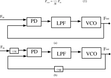
4.2.1 Synthesizer
The block diagram of a typical PLL consists three blocks of (a) Phase Frequency Detector
(PFD), (b) Low Pass Filter (LPF) and (c) Voltage Controlled Oscillator (VCO) as shown
in Fig. 19a. The PFD compares the phase and the frequency of the reference input and the
VCO output to generate an output that is linearly proportional to the phase difference (ΔΦ).
An (LPF) filter is required to suppress the ripples of the control voltage. When the control
voltage is zero, the VCO frequency is set to a center frequency that varies linearly
proportional to the control voltage. The PLL block can readily be modified by adding
divider to design a synthesizer as shown in Fig. 19b. In this case, the relationship between
the frequency of the input reference signal, and the VCO output signal is given by:
in
out F
N M
F (1)
4.2.2 Authentication Controller Block Constitution
The authentication controller presented in this study Fig. 20 is constituted of the following:
an n-bit register, XOR gate, n-bit counter and trial counter. The controller functions as
follows. An n-bit secret key is defined by the designer and stored in the n-bit register in Figure -19 Block diagram of (a) a Conventional PLL and (b) a PLL based Synthesizer
PD
LPF
VCO
Fin
÷
N÷
MF
outPD
LPF
VCO
Fin
F
out
(a)
32
order to be compared against the n-bit tester input using the XOR gate. If the two keys
match each other, pass flag will be raised and the access to the scan chain is granted.
However, in the case of mismatch, a trial counter is incremented. The trail counter is
dedicated to track the number of failures and prevents further attempts after a preloaded
maximum number of trails.
4.2.3 Tester Authentication sequences
The tester authentication is performed in two phases as described below:
1. Phase 1:
The CUT is equipped with a PLL system to synthesize a new frequency equal to Fin (M/N).
Where M and N are two constants known by the designer and Fin is the frequency of the
Voltage Controlled Oscillator (VCO) within the PLL. The CUT sends an interrupt signal
via Dout and waits for the tester to provide the authentication information through Din as
shown in Fig. 18.
2. Phase 2:
The tester receives the synthesized clock signal running at Fin (M/N) frequency. The PLL
has to be able to lock on the signal and generate a clock running at Fout frequency.
Otherwise, the tester and the CUT will operate at different frequencies. As a result, the data Figure -20 Tester Authentication Module
Counter n-bit
Flip Flop n-bit Register
n-bit Tester Input
Access to Scan Chain
Trial Counter Authentication
33
applied to the scan chain by the tester will not propagate within the scan chain properly
due to synchronization problem.
Once the tester successfully captures the lock and synchronizes with the CUT, it sends its
authentication key, which is compared against the content of a preloaded authentication
register to verify the tester. The access to the scan chain will only be provided if the tester
is successfully authenticated. Otherwise, the CUT requests for a valid authentication key.
Contrarily to the reported methods where limitless attempts are allowed to apply input test
pattern to the CUT and observe its responses, the number of attempts is limited in the
proposed solution in this work.
4.3 The Proposed Secure Scan Chain Architecture
In the proposed solution, we define two modes of operation safe mode and test mode. At
the safe mode of operation, the secret key is produced by a group of flip-flops within the
scan chain as shown in Fig. 21. Note that, after the tester has been authenticated, access to
the scan chain is granted. However, to protect the scan chain against possible attacks, the
access to the scan cells is not directly granted in the test mode. This will protect the CUT
from fault injection attacks where the CUT operation mode is abruptly changed from the
test mode to the safe mode to scan out critical information.
Figure -21 Proposed architecture of N-bit secret key at the safe mode
D-FF Scan Chain 1 Clk D Q D-FF 0 D Q D-FF D Q D-FF D Q
N-bit Secret Key
34
Switching the mode of operation to the test one will provide an opportunity for an
unauthorized access. Therefore, a reset signal is proposed to clear the secret key held by
the flip-flops in order to protect it from access by an attacker and to overcome the issue of
power-OFF in [11].
In order to test the circuit, a reconfigurable LFSR is proposed to implement a Built-In
Self-Test (BIST) method. The proposed architecture of reconfigurable LFSR in the test mode
is shown in Fig. 21. The N flip-flops of the scan chain are converted to an n-bit
reconfigurable LFSR to act as an Automatic Test Pattern Generator (ATPG) for the array
of flip-flops configured in the test mode.
The access to the output of the shift register is granted through the scan-chain. This allows
the tester to use the scan chain to capture the data and perform evaluation of the responses.
The data captured is compared against the golden response of the circuit to determine
whether it is fault-free or faulty. The length of the key needed for testing is mainly
determined by the number of the D-flip-flops implemented for the required operation
The proposed reconfigurable LFSR consists of the following: a Multiplexer and an XOR
gate.
Figure -22 Proposed architecture at the test mode in which a reconfigurable LFSR is formed using scan chain flip-flops.
D-FF 1 M U X 1 D-FF 2 D-FF 3 D-FF 4 D-FF 5 D-FF N
1 0 0 1 1 0
35
As shown in Fig. 22, the circuit can be configured for four different lengths of LFSR. The
control bits C1/C2 will determine the length of the LFSR through a 4×1 multiplexer.
However, the configuration might be extended further using a larger multiplexer depending
upon the nature of application required.
4.4 Implementation
Cadence design environment using TSMC CMOS 65nm technology has been used to
implement the proposed solution to secure a scan chain. The level of the complexity
depends on the size of the key register.The total area overhead for implementation of the
proposed solution to secure the scan chain using128-bit secure key and a 32-bits register
for tester authentication is about 1847.05 µm2 as shown in Fig. 23. If the size of the register
key increases, the security of the encryption key increases at the cost of extra area overhead.
4.4.1 Area Overhead
Various solutions have been reported in previous works to secure conventional scan chain
[17, 6]. The area overhead of Lock and Key security solution [17] is reported moderately
low (327 gates) for 4-bit. However, a noteworthy impact on the area overhead (5817 gates)
is reported if the number of bits increases to 12-bit due to the LFSRs and decoders. Figure -23 Area overhead of the proposed solution using TSMC 65nm CMOS
![Figure -1 A wafer of 22nm Ivy Bridge CPUs containing more than a billion transistors [2]](https://thumb-us.123doks.com/thumbv2/123dok_us/1377048.1170387/17.612.109.499.274.485/figure-wafer-ivy-bridge-cpus-containing-billion-transistors.webp)
![Figure -3 Cost (cents/transistor) evolution fabrication and effort for testing [5]](https://thumb-us.123doks.com/thumbv2/123dok_us/1377048.1170387/19.612.106.535.193.448/figure-cost-cents-transistor-evolution-fabrication-effort-testing.webp)
![Figure- 5 Six levels copper metal interconnects of CMOS chip developed by IBM [11]](https://thumb-us.123doks.com/thumbv2/123dok_us/1377048.1170387/20.612.108.540.459.689/figure-levels-copper-metal-interconnects-cmos-chip-developed.webp)
![Figure. 6 (a) 3D IC integration using Through Silicon Vias (TSV) and (b) 16Gb NAND flash stack using TSV developed by Samsung [12]](https://thumb-us.123doks.com/thumbv2/123dok_us/1377048.1170387/22.612.109.542.66.614/figure-integration-using-silicon-vias-using-developed-samsung.webp)