University of Windsor University of Windsor
Scholarship at UWindsor
Scholarship at UWindsor
Electronic Theses and Dissertations Theses, Dissertations, and Major Papers
10-5-2017
High Level Synthesis and Evaluation of an Automotive RADAR
High Level Synthesis and Evaluation of an Automotive RADAR
Signal Processing algorithm for FPGAs
Signal Processing algorithm for FPGAs
Siddhant Luthra
University of Windsor
Follow this and additional works at: https://scholar.uwindsor.ca/etd
Recommended Citation Recommended Citation
Luthra, Siddhant, "High Level Synthesis and Evaluation of an Automotive RADAR Signal Processing algorithm for FPGAs" (2017). Electronic Theses and Dissertations. 7274.
https://scholar.uwindsor.ca/etd/7274
This online database contains the full-text of PhD dissertations and Masters’ theses of University of Windsor students from 1954 forward. These documents are made available for personal study and research purposes only, in accordance with the Canadian Copyright Act and the Creative Commons license—CC BY-NC-ND (Attribution, Non-Commercial, No Derivative Works). Under this license, works must always be attributed to the copyright holder (original author), cannot be used for any commercial purposes, and may not be altered. Any other use would require the permission of the copyright holder. Students may inquire about withdrawing their dissertation and/or thesis from this database. For additional inquiries, please contact the repository administrator via email
High Level Synthesis and Evaluation of an Automotive
RADAR Signal Processing Algorithm for FPGAs
by
Siddhant Luthra
A Thesis
Submitted to the Faculty of Graduate Studies
through the Department of Electrical and Computer Engineering
in Partial Fulfillment of the Requirements for
the Degree of Master of Applied Science
at the University of Windsor
Windsor, Ontario, Canada
2017
High Level Synthesis and Evaluation of RADAR Signal Processing algorithm for FPGAs
by
Siddhant Luthra
APPROVED BY:
__________________________________________
T. Bolisetti
Department of Civil and Environmental Engineering
____________________________________________
E, Abdel-Raheem
Department of Electrical and Computer Engineering
_____________________________________________
M. Khalid, Advisor
Department of Electrical and Computer Engineering
iii
Author's Declaration of Originality
I hereby certify that I am the sole author of this thesis and that no part of this thesis has
been published or submitted for publication.
I certify that, to the best of my knowledge, my thesis does not infringe upon anyone’s
copyright nor violate any proprietary rights and that any ideas, techniques, quotations, or
any other material from the work of other people included in my thesis, published or
otherwise, are fully acknowledged in accordance with the standard referencing practices.
Furthermore, to the extent that I have included copyrighted material that surpasses the
bounds of fair dealing within the meaning of the Canada Copyright Act, I certify that I have
obtained a written permission from the copyright owner(s) to include such material(s) in
my thesis and have included copies of such copyright clearances to my appendix.
I declare that this is a true copy of my thesis, including any final revisions, as approved
by my thesis committee and the Graduate Studies office and that this thesis has not been
iv
Abstract
High Level Synthesis (HLS) is a technology used to design and develop hardware
(HW) using high-level languages such as C/C++. An HLS model of an automotive
RADAR signal processing algorithm has been developed for the purpose of comparison
between the HLS model and the existing HDL model. Register Transfer Level (RTL)
programming is a technology used to design and develop hardware at the register transfer
level (or low level) using Hardware description languages such as Verilog and VHDL.
FPGA development usually requires the knowledge of RTL technologies. HLS gives
software (SW) developers the ability to design and implement their designs on an FPGA
without requiring the knowledge of RTL technologies and HDL.
Even though HLS is currently gaining popularity, the applications used to evaluate
HLS tend to remain small. We synthesize an automotive RADAR signal processing system
using HLS-based design methodology, which has mid to high complexity, and compare
our synthesis results to that of the RTL-based design. We used many techniques used to
make the high-level program model ready for synthesis while optimizing for both speed
and resource usage using Xilinx Vivado HLS Computer-Aided Design (CAD) tool. We
achieved a speed up of 2X compared to the RTL-based design while reducing the design
time from approximately 16 weeks to 6 weeks. The FPGA resource utilization increased
v
Acknowledgements
With utmost sincerity, I express my gratitude and respect to my advisor Dr. M. Khalid,
who gave me the wonderful opportunity to work under his supervision and inspired me to
work with honesty, integrity and discipline.
I would also like to thank my committee members Dr. T. Bolisetti and Dr. E.
Abdel-Raheem, who provided me with insightful suggestions to improve my research.
I would like to dedicate my work to my parents, as their ever-encouraging faith has
kept me going and gave me the strength to overcome any obstacles that have come my
vi
Table of Contents
Author's Declaration of Originality ... iii
Abstract ... iv
Acknowledgements ...v
List of Tables ... viii
List of Figures ... ix
List of Abbreviations ...x
Chapter 1. Introduction ...1
1.1. Motivation ... 1
1.2. Objective ... 2
1.3. Thesis Outline ... 2
Chapter 2. Background ...4
2.1. FPGAs ... 4
2.2. Hardware Design Methodologies... 5
2.2.1. Hardware Design using HDLs ... 6
2.2.2. Hardware Design using HLS ... 8
2.2.2.1. High Level Synthesis Design Methodology ... 10
2.3. Related Research ... 12
2.3.1. High Level Synthesis of an H.264 Decoder ... 13
Chapter 3. Automotive RADAR Signal Processing ...14
3.1. Target Detection using RADAR systems ... 14
3.2. An Automotive RADAR Signal Processing system... 15
3.2.1. RADAR Transmitter and SP3T switch Control ... 17
3.2.2. RADAR Receiver Flow Control and Signal Processing ... 19
Chapter 4. Implementations of the RADAR Signal Processing System ...23
4.1. MATLAB Implementation ... 23
4.2. HDL-Based Implementation ... 31
4.2.1 TLC – Top Level Control ... 31
4.2.2 Sampler ... 33
4.2.3 FFT ... 33
4.2.4 Peak Intensity Calculator (PSD) ... 34
4.2.5 Constant False Alarm Rate Processor (CFAR) ... 34
4.2.6 Peak Pairing Module ... 34
4.2.7 Usage/Timing analysis for the design ... 34
4.3. High Level Synthesis of the RADAR system ... 35
vii
4.3.2. Top-Level Function/Module ... 40
4.3.3. Adc_control() function ... 41
4.3.4. Fft_control() function ... 41
4.3.5. Fft_absolute() function ... 42
4.3.6. Cfar() function ... 43
4.3.7. Peak_pairing() function ... 44
4.3.8. Optimizations and Final Design ... 45
Chapter 5. Synthesis Results ...49
5.1. Approximate Time-To-Market ... 49
5.2. Resource Utilization ... 50
5.3. Performance ... 54
Chapter 6. Conclusions and Future Work ...56
6.1. Summary ... 56
6.2. Future Work ... 56
References ...58
Appendix – Source Code ...60
viii
List of Tables
Table 1 Xilinx 7-series FPGA family comparison [12] ... 5
Table 2 Popular HLS tools ... 9
Table 3 Pragma Class supported by Vivado HLS [2] ... 12
Table 4 Initial System Specifications [5] ... 15
Table 5 Final Parameters for the Algorithm [5] ... 22
Table 6 Specifications for Test 1 (3-Lane Highway with narrow beam) ... 28
Table 7 Results for Test 1 (3-Lane Highway with narrow beam) ... 29
Table 8 Specifications for Test 2 (3-Lane Highway with a single wide beam) ... 30
Table 9 Results for Test 2 (3-Lane Highway with a single wide beam) ... 30
Table 10 FFT Specifications [5]. ... 33
Table 11 Resource utilization on the Virtex-5 board. [5] ... 35
Table 12 Timing/Latency analysis for the HDL-based design ... 35
Table 13 Inputs and Outputs of the main design. ... 36
Table 14 I/O for adc_control() function ... 41
Table 15 I/O for fft_control() function ... 42
Table 16 I/O for fft_absolute() function ... 43
Table 17 I/O for cfar() function ... 44
Table 18 I/O for peak_pairing() function ... 45
Table 19 Resource utilization breakdown ... 51
Table 20 RAM utilization comparison. ... 51
Table 21 Slice LUTs / Registers utilization comparison. ... 52
Table 22 BRAM and DSP blocks utilization comparison. ... 53
ix
List of Figures
Figure 1 Concurrent Operations Example pseudo-code ... 6
Figure 2 Overview of Xilinx Vivado HLS Design Flow ... 10
Figure 3 Conceptual Diagram of the RADAR system [5] ... 16
Figure 4 Flowchart for the RADAR transmitter and SP3T switch control [5] ... 19
Figure 5 Flowchart of Radar Receiver flow control and Signal Processing [5] ... 21
Figure 6 Flowchart of the MATLAB implementation [5] ... 25
Figure 7 Illustration of test scenario 1 (3-Lane Highway with narrow beam) [5]. ... 28
Figure 8 Illustration of test scenario 2 (3-Lane Highway with single wide beam) [5]. ... 29
Figure 9 HDL-based design overview [5] ... 31
Figure 10 TLC overview ... 32
Figure 11 Approximate time taken to write HDL and HLS code. ... 50
Figure 12 RAM utilization comparison graph ... 51
Figure 13 Slice LUTs / Registers utilization comparison graph ... 52
Figure 14 BRAM and DSP blocks utilization comparison graph ... 53
x
List of Abbreviations
FPGA HLS HLL HW SW RTL HDL VHDL VHSIC RADAR CAD IC OTP ASIC SSI CPU GPU DSP IP FFT I/O SoC FPS FM-CW LFM-CW MEMS RF MMIC VCO TLC RPU SP3T ADC DAC CFAR CA-CFAR SNR RAM
Field Programmable Gate Array High Level Synthesis
High Level Language Hardware
Software
Register Transfer Level
Hardware Description Language
VHSIC Hardware Description Language Very High Speed Integrated Circuit Radio Detection And Radio Ranging Computer-Aided Design
Integrated Circuit
One-Time Programmable
Application-Specific Integrated Circuit Stack Silicon Interconnect
Central Processing Unit Graphics Processing Unit Digital Signal Processing Intellectual Property Fast Fourier Transform Input/Output
System On Chip Frames Per Second
Frequency Modulated – Continuous Wave Low Frequency Modulated – Continuous Wave Microelectromechanical System
Radio Frequency
Monolithic Microwave Integrated Circuit Voltage Controlled Oscillator
Top-Level Control Radar Processing Unit Single Pole Three Throw Analog to Digital Converter Digital to Analog Converter Constant False Alarm Rate
Cell-Averaging Constant False Alarm Rate Signal to Noise Ratio
xi ROM
FIFO R&D LUT FF
Read Only Memory First-In First-Out
Research and Development Look Up Table
1
Chapter 1.
Introduction
1.1. Motivation
High Level Synthesis is gaining popularity as a primary design methodology when it
comes to hardware design due to a number of advantages such as higher productivity, faster
time to market, etc. Even though HLS provides many advantages over the current
RTL-based design methodologies, a lot of work remains to be done in effectively utilizing HLS
Computer-aided Design (CAD) tools for hardware design targeting complex real world
applications.
There have been a few case studies in the past which focus on the High-Level Synthesis
of various hardware designs [1, 8] but they generally focus on the design itself and not the
comparative evaluation of HLS results with the older RTL-based design methodologies. A
case study which focuses on the comparison and evaluation of HLS and HDL synthesis
results is presented in [2]. The H.264 video decoding algorithm was synthesized using
Vivado HLS CAD tool [3]. Some previous case studies which focus on the HLS
technology itself have shown promise that HLS is ready for mainstream implementation
[10]. A detailed overview of currently available HLS CAD tools from the industry and
academia is presented in [11, 13]
The main motivation for this thesis is to compare HLS and HDL-based design
methodologies for designing a mid to high complexity design which is the automotive
RADAR signal processing algorithm to detect a target’s range and velocity with respect to
2
1.2. Objective
The main goal of this thesis is to evaluate and compare HLS and HDL-based design
methodologies by simulating and synthesizing an automotive RADAR signal processing
algorithm for Xilinx Virtex 7 FPGA. The metrics used for the evaluation and comparison
are time-to-market, speed (timing analysis), and area (resource utilization). The CAD tool
used for this purpose is the Xilinx Vivado HLS. The HDL model used in our comparison
is described in [4, 5]. For fair comparative analysis, the existing HDL model was updated
to target the Xilinx Virtex 7 FPGA using Xilinx Vivado since the original design was for
the Xilinx Virtex 5.
A few other questions which will be answered in this thesis are:
• Is HLS ready for complex real world applications such as the automotive
RADAR signal processing algorithm?
• What are the advantages of HLS over HDL-based synthesis?
1.3. Thesis Outline
This remainder of this thesis is organized as follows:
In Chapter 2, the background of FPGAs, hardware design methodologies (HDL and
HLS), tools for hardware design, a brief comparison of the technologies, and related
research are briefly discussed. Chapter 3 describes the automotive RADAR signal
processing algorithm to be synthesized using HLS. This includes a brief introduction to
3 In Chapter 4, implementations of the algorithm at different levels of abstraction,
namely, MATLAB, C++, and Verilog are discussed. Chapter 5 discusses the results
obtained from various implementations which are then used for the evaluation and
comparison of the HLS and the HDL-based design methodologies. We finally conclude in
4
Chapter 2.
Background
This chapter provides background information on FPGAs and HLS. Previous related
works are also discussed.
2.1. FPGAs
Field Programmable Gate Arrays (FPGAs) are Integrated Circuits (ICs) which consists
of large amounts of programmable logic resources, programmable routing and embedded
resources such as memories and DSP blocks. FPGAs enable rapid and custom hardware
design for many real-world applications. They are also used for prototyping various
hardware designs before they are sent for IC fabrication. FPGAs enables us to reprogram
the hardware architecture to mimic a custom IC which allows us to do thorough testing
before the design is sent for fabrication. Although one-time programmable (OTP) FPGAs
are available which perform specific tasks, reprogrammable FPGAs are more popular
because they can handle design changes as the design evolves.
Application specific integrated circuits are custom hardware ICs which are
manufactured for specific applications. Although ASICs are faster and consume less
power, the recent advances in FPGAs push the limits of speed, complexity, and physical
size in comparison to older FPGAs.
The FPGA used for this research is the Xilinx Virtex 7, which is one of the four Xilinx
7 series FPGA families. These FPGAs are optimized for highest system performance and
5 devices enabled by stack silicon interconnect (SSI) technology [12]. An overview
comparison between the four different families of Xilinx 7-series FPGAs is shown in Table
1.
Table 1 Xilinx 7-series FPGA family comparison [12]
2.2. Hardware Design Methodologies
Hardware design can be done either for a specific task (Single purpose) or to execute
different multiple tasks (General purpose). General purpose hardware (or IC) is designed
to be able to execute multiple different tasks, the best example would be a CPU in a
personal computer. Single purpose hardware are ICs which are designed only to perform
one task and do it well, a common example for this would an IC for encryption and
decryption. For our research, we will focus on single purpose HW.
There are a few ways to design hardware, it all depends on what the intention of the
design is. For this thesis, we are more concerned about FPGA prototyping which means
that we would program an FPGA to perform certain tasks. Traditionally, a Hardware
description language (HDL) is used to program the FPGA at the RTL level, two most
6 program FPGAs which allows us to do so using High Level Languages (HLLs). This allows
rapid hardware design targeting ASICs and FPGAs.
2.2.1. Hardware Design using HDLs
As mentioned earlier one of the traditional and most popularly used technology to
program FPGAs is using HDLs. They allow the designers to program at the RTL level.
VHDL and Verilog, being the two most popular HDLs, had a huge impact on hardware
development when they were created.
The main feature of HDLs is the ability to model concurrent operations which is
important to reduce the run time of a specific task. It can provide faster speed but is hard
to code and can have stalling issues due to dependencies.
An example of concurrent operations is discussed here:
Figure 1 Concurrent Operations Example pseudo-code
For the example in Figure 1, let’s assume that each addition takes 1 clock cycle and
assigning operations have no delays. If this code is to be run sequentially, Line 1, Line 2,
and Line 3 will take 1 clock cycle each since they have one addition (+) each which means
the whole process will take 3 clock cycles. Now, to run this code in parallel, we come
across with an issue of dependency on Line 3. What this means is to run Line 3, we need
7 statements run. In this case, Line 1 and Line 2 can be run in parallel since both the lines
have no dependencies. To sum it all up, executing Line 1 and Line 2 will take only 1 clock
cycle, and executing Line 3 will take another 1 clock cycle, so it will take 2 clock cycles
instead of 3 when compared to the sequential (or non-concurrent) execution. Even though
there isn’t much difference in the time consumed, this gap increases as the designs get
bigger and more complex. Concurrent programming is one of the most important
techniques a hardware designer requires but can get very complicated while using HDLs.
Another significant feature RTL based designs provide us is access to arbitrary
precision data types, what this implies is every input, output, internal registers, etc. can
have the desired number of bits. In HLLs, however, we usually only have access to data
types bound by 8-bit boundaries. The arbitrary precision data types we have access to has
an effect on the size, speed, precision, flexibility and power consumption of the final
design.
There are quite a few tools available for FPGA programming using HDLs, the one we
will be focusing on is Xilinx Vivado.
Currently, Xilinx Vivado is part of the Vivado Design Suite, created by Xilinx. Since
the FPGA we are using in our thesis is made by Xilinx. This would be the best tool for us
to use. All the Xilinx Vivado Design Suite tools are written with a native tool command
language (Tcl) which offers us access to all the tools via command line which is available
in the GUI. Xilinx Vivado Design suite currently supports the Xilinx® UltraScale™ and 7
series devices, Zynq® UltraScale+™ MPSoC device, and Zynq®-7000 All Programmable
8 As discussed earlier, the FPGA in question for our thesis is from the Xilinx 7 series
called the Virtex 7. Xilinx Vivado is a very broad tool which allows us to synthesize,
implement, simulate and analyze our design. It supports both VHDL and Verilog but we
will be focusing on Verilog since the existing HDL model of the automotive RADAR
signal processing algorithm is written in Verilog.
2.2.2. Hardware Design using HLS
Even though the technologies mentioned in the previous section are very advanced,
recent increases in logic capacity of FPGAs and other similar hardware are making these
technologies somewhat tedious and time consuming. This would mean a very long
time-to-market along with large code size which further implies that the code is more complex
and not particularly readable. Eventually, it comes down to the cost of the product in
development. Higher time-to-market would mean the development cost will be higher. To
overcome the ever-increasing cost and delays in product release, we look for alternatives
to these technologies.
An alternative which we will be considering is High Level Synthesis (HLS). HLS
allows designers to program hardware using HLLs (C/C++/SystemC) which are usually
used for software development. HLS tools, in essence, synthesize the HLL code into
optimized RTL level models but there are substantial differences between the models
created by the code written in HLL and HDL. As seen from a broader perspective, there
are two main types of HLS technologies, one allows us to design the entire hardware in
HLLs, while the other is used to accelerate certain parts of a software using hardware also
known as heterogeneous computing. For example, the automotive RADAR signal
9 A basic example of heterogeneous computing would be: a GPU is used to accelerate 3-D
rendering of graphics for a program running on the CPU. There are various tools available
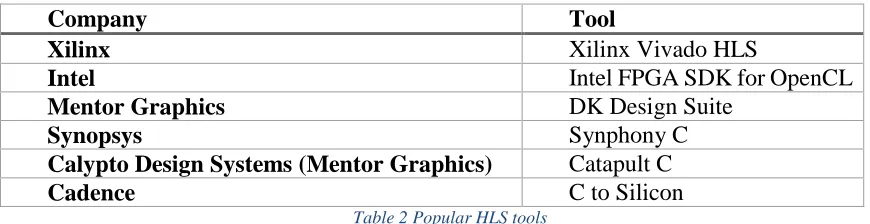
for both types of applications. A few popular ones are shown in Table 2.
Company Tool
Xilinx Xilinx Vivado HLS
Intel Intel FPGA SDK for OpenCL
Mentor Graphics DK Design Suite
Synopsys Synphony C
Calypto Design Systems (Mentor Graphics) Catapult C
Cadence C to Silicon
Table 2 Popular HLS tools
The HLS tool we will be using is Xilinx Vivado HLS which is a part of the Vivado
Design Suite by Xilinx. This tool essentially synthesizes the code written in C, C++ or
SystemC and produces an optimized RTL level model. One important feature of this CAD
tool is the ability to use different C/C++ compilers like GCC to compile the HLL code and
then convert it into the RTL model, this includes the verification for the design using test
benches created in C/C++ or SystemC. The testbench created in HLLs are highly
productive in the sense they require very little time when compared to test benches created
in Verilog, VHDL or SystemVerilog. Since we are using the Xilinx Virtex 7 FPGA board
for our thesis. This tool provides us with all the necessary sub-tools required to successfully
program the automotive RADAR signal processing algorithm for the Xilinx Virtex 7.
Some other features of this tool include the ability to create Intellectual Property (IP)
cores which means we can import sub-designs from other models into our current design
easily. Xilinx provides us with some IP cores like Fast Fourier Transform (FFT), Finite
Impulse Response (FIR) filters etc. These become very important since programming these
10 manually. With these IP cores, Xilinx also provides us with a variety of options in these
cores, since not all designs are going to use the same type of cores. A simple example is
the FFT size, it can be adjusted by setting up the FFT size parameter to suit the design.
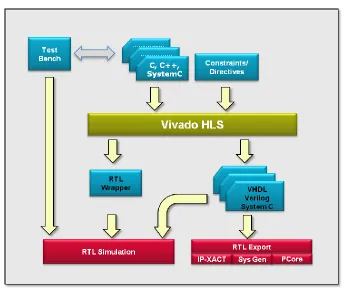
The way Xilinx Vivado HLS works is that it synthesizes the HLL code into an
optimized RTL level model. An overview of Vivado HLS design flow is shown in Figure
2.
Figure 2 Overview of Xilinx Vivado HLS Design Flow
2.2.2.1. High Level Synthesis Design Methodology
The first step in HLS design methodology is to overcome the limitations HLLs have
when it comes to hardware design. Some limitations HLLs have over HDLs are mentioned
11
• In standard HLLs like C/C++, the data types are usually bound by 8-bit
boundaries (8, 16, 32, and 64 bits). Whereas HDLs supports data types with
arbitrary bit-lengths [17, 18, 19].
• One of the main features of HDLs is concurrent (or parallel) programming.
Since HLLs like C/C++ revolve around the concept of sequential programming,
special tools are required to program concurrent functions (or modules).
• Standard HLLs do not have the ability for memory management for the entire
hardware.
Most HLS CAD tools, including Xilinx Vivado HLS, have pre-built libraries and
inbuilt features to overcome most of the limitations HLLs have when it comes to
programming for hardware design. Some of the features which are part of the Xilinx
Vivado HLS are [13, 16]:
• Vivado HLS automatically generates the Input/output (I/O) interfaces for the design
with memories or other communication interfaces.
• It also allocates the necessary registers, memory access, scheduling of operations
and binding these operations to the respective functional units.
• Vivado HLS uses pragmas to promote further optimizations using various
techniques like flow optimization, loop pipelining, array partition etc., the pragma
class supported by the tool can be seen in Table 3 [2].
• Vivado HLS provides us with pre-built libraries which include arbitrary precision
(for integers) and arbitrary fixed point precision (for fractional numbers) data types
for C/C++. This allows variables of arbitrary widths ranging from 1-bit to
12
Pragma Class Operation
Interface Define function interface Function Call Function Inlining/off
Flow Optimization
Separate instantiation of functions Loop Optimization Loop pipelining
Loop unrolling
Loop merge operations Memory Control Array partition, etc.
Table 3 Pragma Class supported by Vivado HLS [2]
The features mentioned above and the automatically applied optimizations by Vivado
HLS are the key design optimization techniques for HLS. Many hardware designers are
moving towards HLS with C/C++ as a primary design language since C-level design and
verification is relatively easy to use, the time-to-market is significantly lower and the final
design is more optimized. The automotive RADAR signal processing algorithm is
synthesized to work as a stand-alone hardware due to the nature of the design. Although
this design is somewhat complex, we will be using top-down approach since all the
functions/modules in our design will be tailored to output the desired results efficiently.
We present details of our HLS based methodology to synthesize the automotive RADAR
signal processing system in Chapter 4.
2.3. Related Research
There have been a few evaluations of HLS or HLS based CAD tools [2, 10, 11, 13, 16].
Most of them evaluate the tool itself using either a particular benchmark [11], or they
conduct surveys and collect information on how HLS has been implemented. However,
13 are focusing on complex applications, we will briefly summarize HLS based design of an
H.264 Decoder [2].
2.3.1. High Level Synthesis of an H.264 Decoder
Many major platforms like YouTube use H.264 as a video coding standard, due to
this the H.264 is present in most of the common embedded SoCs such as Apple’s
mobile processors, and the popular Qualcomm Snapdragon processors. H.264 being a
very complex application, demands HLS-based design so that the designers can achieve
accurate results without the tedious and time consuming nature of HDL-based designs.
An H.264 decoder has been synthesized using HLS techniques in [2]. The desired
design was required to achieve a throughput of 542 frames per second (fps) at 176x144
resolution and 34 fps at 640x480 (480p) resolution. The results obtained [2] using HLS
satisfy the targeted throughput, which shows that HLS-based design methodologies are
effective even with complex applications like video decoding. Due to the rapid
advancements in HLS-based CAD tools, HLS-based design methodology is
increasingly becoming popular and may become a standard for hardware design in
future.
A top-down approach for the open-source C-reference model for the H.264 decoder
was used. Code restructuring and performance optimizations were performed on the
C-reference model in [2], ensuring efficiency while obtaining the desired results. Since
the desired throughput was successfully achieved in [2], we used similar optimization
techniques to get the desired result for the automotive RADAR Signal Processing
14
Chapter 3.
Automotive RADAR Signal Processing
3.1. Target Detection using RADAR systems
Detecting targets for various scenarios in vehicles plays an important role in collision
avoidance for automobiles. Although Collison avoidance in vehicles is one of the many
applications for target detection, it is an important one since on-road safety has always been
a high priority. All the global auto industries are extensively pursuing RADAR based target
detection for various purposes like collision warning, automatic braking, blind spot
monitoring, parking aid, adaptive cruise control, lane change assistance, and rear crash
Collison warning and avoidance, etc. Target detection using various methods like RADAR
are extensively being researched while designing autonomous vehicles.
Earlier, a high-power Pulsed Doppler RADAR technique was relied upon for target
detection, although this technique was criticized due to the failure of the Mercedes-Benz
pulsed RADAR assisted Distronic cruise control system [5]. Therefore, new techniques
like the Frequency Modulated-Continuous Wave (FM-CW) RADAR was introduced.
Automotive RADAR systems have proved very reliable in recent years in reducing the
number of fatal accidents. Initially, these systems were expensive to implement and were
only available in high-end luxury cars. Due to the advances in hardware technologies, the
costs of implementing these systems in the automotive industry have been reduced
significantly. This enables lower-end vehicles to be equipped with the collision avoidance
15
3.2. An Automotive RADAR Signal Processing system
The automotive RADAR signal processing system we will be focusing on is presented
in [5]. The system is based on the Long Range Automotive system developed at the
University of Windsor. It measures the target range and velocity based on the Linear
FM-CW (LFM-FM-CW) approach using a Microelectromechanical system (MEMS) Rotman Lens,
MEMS Radio Frequency (RF) switches and phased array antennae for transmission and
reception of the signal which the algorithm will process to get the desired output. Table 4
provides the initial system specifications of the automotive RADAR signal processing
system [5].
Parameter Value
RADAR Type LFM-CW
Operating Frequency 77 GHz
Voltage Controlled Oscillator (VCO) TLC77xs*
Target Model(s) considered Swerling I, III, and V type targets
Beamformer Rotman Lens
Number of Beams 3
Processing duration per beam 2 ms
Beam Width ±4.5°
Antenna Type Phased Array Antenna
RADAR Processing unit (RPU) platform
FPGA
16
Figure 3 Conceptual Diagram of the RADAR system [5]
A conceptual diagram of the entire RADAR system, showing the major components
can be seen in Figure 3. In this design, we will be focusing on the RADAR processing unit
which is the FPGA. As we can see, the RPU or the FPGA has 3 main outputs and 1 main
input.
The three main digital outputs are:
1. Output to the 77 GHz VCO.
2. Output to the Single Pole 3 Throw (SP3T) switch.
3. Output representing the target velocity and range.
The only main input is the time-domain sample received from the Analog-to-Digital
17 The RADAR Signal Processing algorithm [5] which is to be synthesized can be divided
into two parts:
1) RADAR Transmitter control and SP3T switch control.
2) RADAR Receiver Flow Control and Signal Processing.
3.2.1. RADAR Transmitter and SP3T switch Control
This section of the algorithm provides the necessary outputs to the VCO and the SP3T
switch. The VCO controls the signal to be transmitted by the RADAR system, and the
SP3T switch is responsible for switching between the MEMS Rotman lens beam ports
(Beam port 1, Beam port 2, Beam port 3).
This part of the algorithm is responsible for the following:
• Generation of the RADAR frequency chirp by tuning the VCO with a voltage
sweep through a Digital-to-Analog Converter (DAC).
• The synchronization of the chirp generation with the signal processing done after
receiving the appropriate signal.
• Keeping track of when every down sweep ends so the appropriate output can be
sent to the SP3T switch control to switch to the next beam port changing the beam
direction.
• Modifying the output to the SP3T to switch between the MEMS Rotman lens beam
ports.
o Beam port 1 to Beam port 2
o Beam port 2 to Beam port 3
18 The flowchart for this part of the algorithm can be seen in Figure 4 [5]. Some key
information regarding this part of the algorithm is listed as follows [5]:
• The sensor begins with beam port 1 of the Rotman Lens, and after system reset.
• The system starts with the up sweep or a positive frequency chirp.
• Based on the market availability of fast DACs, a 10-bit DAC with a 900
nanoseconds refresh period should be suitable for the target sweep duration of 1
millisecond.
• The DAC is configured to output voltage range from 4.5 V to 6.1 V based on the
10-bit modulating output to the DAC from the FPGA which ranges from 0 to 1023.
• A clock signal is also sent to the DAC for the DAC clock.
• A sampling clock for the ADC will be sent to the ADC.
• The output to the 3-pin MEMS RF switch control will be a 3-bit output from the
FPGA:
o (100)2 (Decimal equivalent of 4): For beam port 1
o (010)2 (Decimal equivalent of 2): For beam port 2
19
Figure 4 Flowchart for the RADAR transmitter and SP3T switch control [5]
3.2.2. RADAR Receiver Flow Control and Signal Processing
This is the main part of the automotive RADAR signal processing algorithm, which
outputs the target information. The input to this are the time-domain samples received from
20
• Applying the Hamming window to the received time-domain samples from the
ADC.
• Perform Fast Fourier Transformation (FFT) on the windowed time-domain
samples to convert into frequency-domain samples.
• Calculating the peak intensity for every frequency bin of the frequency-domain
samples.
• Neglecting noise, clutter, and individual target detection by running a Constant
false alarm rate (CFAR) algorithm for both up and down sweeps.
• Calculate the final target information by peak pairing, after the CA-CFAR
algorithm is done.
The flowchart for the RADAR receiver flow control and Signal Processing can be seen
in Figure 5 [5]. Some key information about this part of the algorithm is listed as follows
[5]:
• The bandwidth of the system was chosen to be 800 MHz for a respectable range
resolution.
• The sampling frequency of 2 MHz was calculated to be used over 1.024 ms for
2048 samples.
• The FFT size, which is the number of samples will be 2048, therefore, 2048
samples will be collected in 1.024 ms.
21
• Since the output from the FFT is symmetrical, only half of the FFT output is
considered therefore the CA-CFAR algorithm processes 1024
frequency-domain peaks.
• The probability of false alarm was selected as 10-6, the averaging depth of 4
cells on either side of the CUT and 2 guard bands on either side of the CUT
were chosen, which generates a scaling constant of approximately 1.3714.
• Spectral proximity and Power level were the two criteria used for peak pairing.
22 The final design specifications for the complete algorithm can be seen in Table 5. These
specifications will be used for the three implementations of the automotive RADAR signal
processing system in Chapter 4.
Parameter Value
LFM-CW sweep bandwidth 800 MHz
FFT size 2048
FFT type Radix-4 DIT
Up/Down sweep duration 1 ms
ADC resolution / Sampling rate 11 bits / 2.2 MSPS
DAC resolution / refresh period 10 bits / 2.2 MSPS
Target range 0.40m – 200m
Target relative velocity ±300 km/h
CFAR Algorithm CA-CFAR
CFAR Parameters One-sided cell-averaging depth = 4
One-sided guard band count = 2
23
Chapter 4.
Implementations of the RADAR Signal Processing
System
This chapter describes the implementations of the automotive RADAR signal
processing algorithm at different levels of abstraction.
1. MATLAB Implementation: This section discusses the MATLAB
implementation of the algorithm, focusing only on the 2nd part of the algorithm
which is the RADAR receiver flow control and signal processing.
2. Existing Verilog Implementation: This section briefly explains the current
HDL implementation of the algorithm [5, 6] targeted for the Xilinx Virtex 5,
and the changes we made to this implementation to target the Xilinx Virtex 7.
3. HLS Implementation and Optimizations: Here we describe the design
methodology we used to implement the automotive RADAR signal processing
algorithm using HLS. This section also covers the various HLS code
optimization techniques we used to make our design more efficient.
4.1. MATLAB Implementation
A MATLAB implementation of the algorithm was used for testing the correctness of
the algorithm using MATLAB version R2016b [20]. The MATLAB design from [5],
creates a MATLAB model to do two things:
24 2. To create sample 10-bit input data which is to be sent to the HDL/HLS based
implementations for simulation.
In [5], three tests have been conducted on MATLAB, the first one is the test to see if
the hamming window function is necessary, and 2 highway test scenarios to check the
accuracy of the signal processing algorithm. A brief explanation of these tests is discussed
in this section. The MATLAB implementation does not test the first part of the algorithm
which is the RADAR transmitter control and SP3T switch control.
Before we discuss the test scenarios, some parameters used for the MATLAB
implementation are as follows:
1. Frequency sweep bandwidth (B) = 800 MHz
2. Sampling Frequency = 2 MHz
3. Sampling duration (T) = 1.024 ms
4. Number of time-domain samples = 2048
5. FFT size = 2048
6. FFT frequency resolution = 2 MHz / 2048 = 976.5625 Hz/bin
7. Rate of change of frequency over a single sweep (k) = Bandwidth/Sampling
duration (B/T).
A flowchart of the sequential MATLAB implementation used for the simulation of the
25
26 Scenario to tests the need for Windowing [5]:
This test verifies the requirement of the windowing stage of the RADAR signal
processing algorithm.
The test scenario used for this is 1 target at 142 meters with the velocity of 165 km/h,
while the host velocity is 70 km/h. Due to the receding target, the relative velocity will be
(70 - 165) = -95 km/h (negative Doppler shift) [5]. Assuming c = 2.973 x 10⁸m/s2.
Results without windowing:
Calculated Up-sweep frequency (fup): 734375.00 Hz
Calculated Down-sweep frequency (fdown): 761718.75 Hz
Calculated target range:
𝑟 =𝑓𝑢𝑝+ 𝑓𝑑𝑜𝑤𝑛
2 ×
𝑐 2𝑘
Therefore, the range r = 142.33 m
Calculated relative target velocity:
𝑣𝑟 =
𝑓𝑢𝑝+ 𝑓𝑑𝑜𝑤𝑛
4 ×
𝑐 𝑓0
Therefore, the velocity vr = -26.497 m/s = -95.39 km/h.
Results with windowing:
27 Calculated Down-sweep frequency (fdown): 760742.11 Hz
Calculated target range:
𝑟 =𝑓𝑢𝑝+ 𝑓𝑑𝑜𝑤𝑛
2 ×
𝑐 2𝑘
Therefore, the range r = 142.15 m
Calculated relative target velocity:
𝑣𝑟 =
𝑓𝑢𝑝− 𝑓𝑑𝑜𝑤𝑛
4 ×
𝑐 𝑓0
Therefore, the velocity vr = -26.497 m/s = -95.39 km/h.
Based on these results, there was no change in the velocity measurement of the
algorithm. However, the measured range distance had a difference of 18 cm, between with
and without windowing. Calculating error percentages for both:
Without windowing: (142.33 – 142)/142 x 100 = 0.23%.
With windowing: (142.15 - 142)/142 x 100 = 0.11%.
Therefore, applying the hamming window to the time-domain samples is a significant
improvement in terms of range measurement. These results also agree with the results of
the similar test in [5].
Scenarios for the verification of the algorithm [5]:
Test 1 (3-Lane Highway with narrow beam): The scenario for this is illustrated in Figure
28
Figure 7 Illustration of test scenario 1 (3-Lane Highway with narrow beam) [5].
The host velocity considered is 70 km/h, 6 targets will be tested, and a 3-beam Rotman
lens RADAR sensor is being used. A Signal to Noise Ratio (SNR) of 4.73 dB was used.
The specifications for this test scenario are mentioned in Table 6.
Beam
Port Target
Range (m)
Velocity (km/h)
Theoretical Up Sweep IF (Hz)
Theoretical Down Sweep IF
(Hz)
1 1 12 65 63784 62358
3 54 24 290397 277280
2 4 111 90 580509 586212
6 90 150 461541 484354
3
2 35 250 158148 209477
5 75 99 405783 414053
6 90 150 461541 484354
Table 6 Specifications for Test 1 (3-Lane Highway with narrow beam)
The results for this scenario with the error percentages of the algorithm are shown in Table
29 Beam
Port Target
Real Range
(m)
Real Velocity
(km/h)
Calculated Range
(m)
Range Error (m)
Calculated Velocity
(km/h)
Velocity Error (km/h)
1 1 12 65 12.36 0.36 66.59 1.59
3 54 24 54.35 0.35 25.71 1.71
2 4 111 90 111.30 0.30 90.44 0.44
6 90 150 90.21 0.21 148.36 1.64
3
2 35 250 35.30 0.30 247.15 2.85
5 75 99 78.32 0.32 100.66 1.66
6 90 150 90.30 0.30 151.76 1.76
Table 7 Results for Test 1 (3-Lane Highway with narrow beam)
The maximum errors for this scenario are:
Range: For target 1 detected at beam port 1 = 0.36 m or (0.36/12) x 100 = 3%.
Velocity: For target 2 detected at beam port 3 = 2.85 km/h or (2.85/250) x 100 = 1.14%.
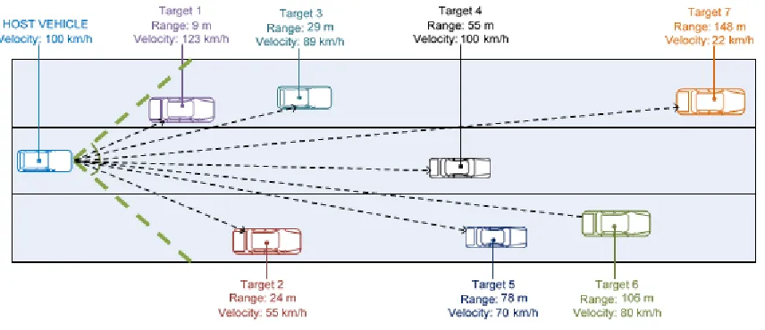
Test 2 (3-Lane Highway with a single wide beam): The scenario for this is illustrated in
Figure 8.
Figure 8 Illustration of test scenario 2 (3-Lane Highway with single wide beam) [5].
30 The host velocity considered is 70 km/h, 7 targets will be tested with a single wide
beam. A Signal to Noise Ratio (SNR) of 4.73 dB was used. The specifications for this test
scenario are mentioned in Table 8.
Target Range (m)
Velocity (km/h)
Theoretical Up Sweep IF (Hz)
Theoretical Down Sweep IF
(Hz)
1 9 123 44004 50563
2 24 55 132585 119753
3 29 89 153990 150853
4 55 100 289060 289060
5 78 70 414239 405684
6 106 80 559964 554261
7 148 22 789013 76671
Table 8 Specifications for Test 2 (3-Lane Highway with a single wide beam)
The results for this scenario with the error percentages of the algorithm are shown in Table
9. Target Real Range (m) Real Velocity (km/h) Calculated Range (m) Range Error (m) Calculated Velocity (km/h) Velocity Error (km/h)
1 9 123 9.38 0.38 123.85 0.85
2 24 55 24.34 0.34 52.31 2.69
3 29 89 29.27 0.27 89.78 0.78
4 55 100 55.37 0.37 100.00 0.00
5 78 70 78.32 0.32 69.34 0.66
6 106 80 106.28 0.28 79.56 0.44
7 148 22 148.37 0.37 21.64 0.36
Table 9 Results for Test 2 (3-Lane Highway with a single wide beam)
The maximum errors for this scenario are:
Range: For target 1 = 0.38 m or (0.38/12) x 100 = 3.167%.
31
4.2. HDL-Based Implementation
The HDL-Based model’s overview can be seen in Figure 9, the HDL for this design is
Verilog. The design is synthesized and simulated using Xilinx Vivado. The original design
from [5] was originally designed for the Xilinx Virtex-5 FPGA but has been updated for
the Xilinx Virtex-7.
Figure 9 HDL-based design overview [5]
4.2.1 TLC – Top Level Control
The Top-Level Control (TLC), is responsible for providing the basic control for the
design. This includes the VCO tuning based on the modulating clock, the sampling clock
to the ADC and the sampler, and the SP3T switch control. The TLC is the main control
32
Figure 10 TLC overview
The 22-bit target information output consists of:
• Most significant 10 Bits: 10-bit target velocity, where 9 bits are used for the integer
part and 1 bit for the fraction, therefore, the velocity is [9-bits].[1-bit].
• The next 10 bits: 10-Bit target range, where 8 bits are used for the integer part and
2 bits for the fraction part, therefore, the range is [8 bits].[2-bits].
• The last 2 bits: The last 2 bits of the final information includes the beam port
number from which the target was detected.
o 01: For beam port 1 (100).
o 10: For beam port 2 (010).
o 11: For beam port 3 (001).
The 10-bit modulating output to DAC controls the VCO voltage based on the DAC
clock.
The 3-pin MEMS RF switch control controls the beam port from which the next
up/down sweep data will be received from the ADC.
33 The sampling clock to ADC is a 2 MHz clock which is the operating clock frequency
of the ADC.
4.2.2 Sampler
The sampler or the ADC-control is responsible for receiving the data from the ADC,
while also providing the necessary logic for the 2 MHz sampling clock to the ADC. The
sampler is also responsible for applying the hamming window function to the time-domain
inputs received from the ADC. The data is then stored in a dual-port RAM which allows
us to access the stored windowed data from the next module.
4.2.3 FFT
The FFT module is responsible for performing the Fast Fourier transform on the
windowed time-domain data from the Sampler. Due to the symmetrical nature of the
Frequency domain data from the FFT, the first 1024 values are ignored by the system since
it also contains more noise. The last 1024 frequency-domain output from the FFT core is
then stored in another dual-port RAM. The specifications of the FFT core can be seen in
Table 10.
Parameter Value
FFT size 2048
Architecture type Burst I/O
Radix Radix-4
Input word length 12 bits
Output word length 12 bits (scaled)
Scaling type Rounding
I/O data type 2’s complement Internal phase factor length 16 bits
34
4.2.4 Peak Intensity Calculator (PSD)
The peak intensities for all the 1024 frequency domain data from the FFT are
calculated here. Before sending the peak intensities forward to the CFAR processor, they
are passed through a square-law detector unit which ensures positive peak intensities for
the entire data.
4.2.5 Constant False Alarm Rate Processor (CFAR)
The CA-CFAR algorithm is implemented in this block. The CFAR processor
receives the data from the PSD in batches of 4 and then stored in a Block-Ram. Once 32
frequency-domain values are received by this block. The CA-CFAR algorithm removes
the unwanted clutter and noise due to the various reasons like system noise and weather
conditions.
4.2.6 Peak Pairing Module
This module is responsible for pairing the peak intensities to detect valid targets
from the CFAR processed frequency domain data. The criteria used for peak paring are
Spectral proximity and power level comparison. The output from this module contains the
target information (velocity, range, and beam port) and is sent to the TLC for the final
adjustments and then sent as an output to the final design.
4.2.7 Usage/Timing analysis for the design
The resource utilization of the original RTL-based design for the Xilinx Virtex-5 board
35
Resource Used Available % Usage
Slice Registers 1357 32640 4 %
Slice LUTs 7445 32640 22 %
DSP48E slices 17 288 5 %
Fully used LUT-FF pairs 705 8097 8 %
BUFG/BUFGCTRLs 1 32 3 %
FPGA fabric area ratio 21 100 21 %
Table 11 Resource utilization on the Virtex-5 board. [5]
Operation Effective Clock cycles per
beam
Latency per Beam with operating Clock at 100 MHz (in ms)
Up sweep sampling 204756 2.047560 ms
Window and feed time-domain samples to FFT core
2072 0.020720 ms
FFT calculation 3960 0.039600 ms
Peak Intensity
Calculations
10743 0.10743 ms
CFAR processing and Peak Pairing
4388 0.060460 ms
Total Signal Processing Latency
21163 0.211630 ms
Overall Latency 225928 2.259280 ms
Table 12 Timing/Latency analysis for the HDL-based design
4.3. High Level Synthesis of the RADAR system
The basic structure for the HLS-based design was kept the same to ensure a fair
comparison between the HLS and HDL-based design. The basic structure for the design is
shown in Figure 9. This section discusses the design methodology used for HLS. The
design was synthesized and simulated using Xilinx Vivado HLS and the FPGA we selected
36 The list of the inputs and outputs for our design is similar to the ports for the
RTL-based design and are shown in Table 13.
I/O Port Name Width (in bits) Description
Inputs
Reset 1 System Reset
Unit_vel 8 Host Velocity in km/h
Data_in 11 Input Data from the ADC
Outputs
Sclk 1 Clock for ADC
Beamport 3 The beam port signal to switch the
S3PT switch
Modulate 10 Modulation output for VCO tuning
Final_target_info 22
Target information which includes target velocity, target range and the beam port in which the target was detected.
Final_info_valid 1 Flag to indicate valid
final_target_info
Table 13 Inputs and Outputs of the main design.
4.3.1. HLS programming techniques
Some features which are important for hardware design are not present in standard
HLLs. Since we are using C++, Xilinx Vivado HLS provides us with some useful
techniques to overcome this limitation. Some of the features [8] we used to program the
design are:
1. Arbitrary Precision
• Data types in standard HLLs like C++ only allow the programmer to use data
with 8-bit boundaries, for example, integers can be represented as either 32 bits
or 64-bits for newer systems.
• Due to the importance given to bit length in hardware design to preserve
37 precision allows us to use variables with arbitrary precision. Xilinx Vivado HLS
currently supports bit-widths from 0 to 1024.
• There are two basic data types for arbitrary precision
i. For Integers: ap_int or ap_uint are two data types which are available to
us. The data width (in bits) is mentioned when these data types are
initialized, for example: ap_int<5> would be a 5 bit signed integer.
ii. For Non-integer numbers: ap_fixed and ap_ufixed are two data types
which are available to us for fraction numbers. The data width (in bits)
for the entire number and the data width of the integer part are
mentioned during initialization of the variable. For example:
ap_fixed<20, 12> would be a 20-bit value with 12 bits for the integer
part and 8 bits for the fraction part.
• These data types allow us to work with variables which are not bounded by the
8-bit boundary. These data types also include member function which returns
the value in different data types for type casting or performing operations. A
few of these member functions are:
i. to_[u]int(): This function returns the [un]signed integer represented by
the arbitrary precision type.
ii. to_[u]double(): This function returns the [un]signed floating point
value.
iii. range(A, B): This function returns the value represented by the bits A to
B. The return type for this function is the same data type as the original
38 2. Multiple outputs from a function
• In standard C++, functions are only allowed to return one type of data, this data
could be an integer, floating point number, or an array etc. In hardware design,
however, there are usually more than 1 outputs, therefore, there are techniques
which are used to support multiple output behavior.
• In Xilinx Vivado HLS, the compiler detects when the values to a function are
passed by value or by reference.
i. The data passed by value to a function are automatically assigned as
Input ports.
ii. The data passed by reference can be assigned as inputs, outputs, or
bi-directional input/output ports based on how they are being accessed
inside the function. If there are writes to this particular reference and no
reads, they are assigned as output ports. If there are reads and no writes,
they are assigned as input ports, and if they are being read from and
written to, they are assigned as I/O ports.
• Therefore, we use pass by value for the inputs and pass by reference for outputs
and I/O ports.
3. Registers
• In C++, there are no available data types which mimic a register in a hardware.
These registers are important since they retain information which were acquired
during the last function run.
• Xilinx Vivado HLS uses static variables for register initialization so the
39
• To use this, “static” keyword is used before the variable initialization. For
example, “static int a = 0;”. The variable “a” in this example will only initialize
once. Once this variable is written to, the value stored in “a” will be maintained
for the next function run.
4. Memory Interface
• In C++, the memory interface equivalent are arrays. Arrays are blocks of data
which can store multiple values of the same data type.
• Random Access memory (RAM) equivalent, these would be regular arrays and
Vivado HLS automatically recognizes if there are both reads and writes to the
array. If there are only read operations for an array they would be treated as
Read-only memory (ROM).
• Read-Only Memory (ROM): Even though Vivado HLS automatically
recognizes if an array is RAM or ROM based on the type of access it has, some
arrays can be forced to be treated as ROMs by adding the keyword “const”
before the array initialization. For example: “const int[5];” would be an array
which stored 5 integer values and will be treated as ROM which implies that
this array will only be written to once. The reason to use this memory interface
is that it takes less time to access data from a ROM than the time taken to access
data from a RAM.
All these additional features help us design efficient and proper hardware using HLLs
40
4.3.2. Top-Level Function/Module
The top module for our design is a function called “RPU()”, the inputs and outputs for
this function are shown in Table 13. We used arbitrary precision data types for all the
inputs, outputs, and the internal registers. For 1 bit internal flags, data type “bool” was
used which are 1-bit data types by default and can have “true” or “false” as their values.
The reason for this is that “bool” types in C++ are very well managed when it comes
to condition management like if-else statements etc. This function, similar to the
RTL-based design, is responsible for VCO tuning, beam port switching, final target
information management. The clock for the ADC is also managed by this function.
This function also calls the necessary functions for further calculations. The
function calls from this function are:
• Adc_control(): This function is called to store the input data from the ADC.
• Fft_control(): This function is called after data for each sweep is collected and
the FFT computation can be started.
• Fft_absolute(): This function is called after the FFT computation has been
completed to store and forward the frequency domain data for further
calculations.
• Cfar(): This function is called for the CA-CFAR computations [5].
• Peak_pairing(): This function is called to detect valid targets and calculations
for the range and velocity of the target [1, 5].
After these functions, the final target information is filled and the final information
41 The input and output of this function are the main I/O for our design which are shown
in Table 13.
4.3.3. Adc_control() function
This function is responsible to store the input data from the ADC. The Hamming
window is applied to the input data and sent to the fft_control() function to be stored. The
Hamming window coefficients are stored in a constant array (ROM) of size 1024 and stores
10-bit window coefficients. These values are acquired using MATLAB. This function
multiplies the input data by the window coefficient and then rounded to 12 bit signed values
and sent to the fft_control() for further computations. The inputs and outputs for this
function can be seen in Table 14.
I/O Port Width (in
bits) Description
Inputs Reset 1 System Reset
Data_in 11 Input Data from the ADC
Outputs
Xn_index 11 Index to maintain the number of data
acquired from ADC.
Xn_value 12 Windowed time-domain data
Fft_start 1 Flag to start FFT computation
Fft_record 1 Flag to indicate fft_control needs to store the windowed data
Table 14 I/O for adc_control() function
4.3.4. Fft_control() function
This function is responsible for storing the windowed time-domain data from the
adc_control(). Once 2048 values have been stored in a First-In-First-Out(FIFO) memory
interface, the FFT computation is started and the output is stored in another FIFO. The
output data which is the frequency-domain values are complex variables. Since we only
42 square root of the sum of squares of the real and the imaginary part. These absolute values
are then sent to fft_absolute() function for further computations. The inputs and outputs for
this function can be seen in Table 15.
I/O Port Width (in bits) Description
Inputs
Reset 1 System Reset
Fft_record 1 Flag to indicate that this function should store the windowed data from adc_control()
Fft_start 1 Flag to indicate FFT computations can be started
Xn_index 11 The index where the data will be stored in the FIFO
Xn_value 12 The value which will be stored at xn_index
in the FIFO
Outputs
Xk_abs 13 The absolute value of the frequency domain
data.
Xk_index 11 The index indicating the number of data currently been sent in xk_abs
Fft_done 1 Flag to indicate FFT computations are
finished
Table 15 I/O for fft_control() function
4.3.5. Fft_absolute() function
This function is responsible for storing 4 absolute values of the frequency-domain data
and are sent to the cfar() function for CA-CFAR computation. Since CFAR works with
bins of 32 values at a time, we send 4 values at a time so this function runs 8 times before
CFAR computation begins. The inputs and outputs for this function can be seen in Table
43
I/O Port Width (in bits) Description
Inputs
Reset 1 System Reset
Fft_done 1 Flag to indicate FFT computations are
finished
Xk_index 11 The index indicating the number of
data currently been sent in xk_abs
Xk_abs 13 The absolute value of the frequency
domain data.
Outputs
outA, outB,
outC, outD 13
4 absolute values to be sent to the cfar() function
Abs_done 1 Flag to indicate that 4 values are being
sent.
Table 16 I/O for fft_absolute() function
4.3.6. Cfar() function
This function is responsible for CA-CFAR computations which store the left and right
averages of a particular frequency bin of 32 frequency-domain data to remove noise and to
detect a new target. Once these computations are done, a new target flag is set to true if a
target has been detected. The absolute value of the particular target and the information
regarding where it was detected is then sent to peak pairing for the range and velocity
44
I/O Port Width (in bits) Description
Inputs
Reset 1 System Reset
inA, inB,
inC, inD 13
4 absolute values to be sent to the cfar() function
Start 1 Flag to indicate that 4 values are being sent. (abs_done output from fft_absolute())
Outputs
Target_abs 13
The absolute value of the frequency domain data of the corresponding detected target
Target_pos 10 The position of the target in the frequency bin where it was detected.
New_target 1
Flag to indicate a new target has been detected and the values in target_abs and target_pos are valid.
complete 1
Flag to indicate that the CFAR computations have been completed for the particular frequency bin.
Table 17 I/O for cfar() function
4.3.7. Peak_pairing() function
This function is responsible to validate the detected targets from the previous functions
and calculate the range and velocity of the target in respect to the host vehicle. This function
waits for the previous computation of each bin and calculates the ranges and velocity of
the detected targets in each bin. Peak pairing allows us to validate the targets and avoid the
spectral copies of a valid target to prevent multiple outputs for the same target. This
function uses spectral proximity and power level comparison as criteria for the necessary
computations. The calculated range and velocity are adjusted and sent to the top level
function (RPU()) for the final output. The inputs and outputs for this function can be seen
![Table 4 Initial System Specifications [5]](https://thumb-us.123doks.com/thumbv2/123dok_us/1373663.1170062/27.612.110.535.408.603/table-initial-system-specifications.webp)
![Figure 3 Conceptual Diagram of the RADAR system [5]](https://thumb-us.123doks.com/thumbv2/123dok_us/1373663.1170062/28.612.125.560.69.342/figure-conceptual-diagram-radar.webp)
![Figure 4 Flowchart for the RADAR transmitter and SP3T switch control [5]](https://thumb-us.123doks.com/thumbv2/123dok_us/1373663.1170062/31.612.175.475.73.487/figure-flowchart-radar-transmitter-sp-t-switch-control.webp)
![Figure 5 Flowchart of Radar Receiver flow control and Signal Processing [5]](https://thumb-us.123doks.com/thumbv2/123dok_us/1373663.1170062/33.612.172.490.281.651/figure-flowchart-radar-receiver-flow-control-signal-processing.webp)
![Table 5 Final Parameters for the Algorithm [5]](https://thumb-us.123doks.com/thumbv2/123dok_us/1373663.1170062/34.612.109.538.163.363/table-final-parameters-algorithm.webp)
![Figure 6 Flowchart of the MATLAB implementation [5]](https://thumb-us.123doks.com/thumbv2/123dok_us/1373663.1170062/37.612.274.393.61.676/figure-flowchart-matlab-implementation.webp)
![Figure 7 Illustration of test scenario 1 (3-Lane Highway with narrow beam) [5].](https://thumb-us.123doks.com/thumbv2/123dok_us/1373663.1170062/40.612.97.554.379.548/figure-illustration-test-scenario-lane-highway-narrow-beam.webp)