Implementation of floating gate MOSFET in inverter for threshold
voltage tunability
F.A.S. Musa1,*, Nurulain D.1, N. Ahmad1, M. Mohamad Isa1and Muhammad M. Ramli1
1School of Microelectronic Engineering, Universiti Malaysia Perlis, Kampus Pauh Putra, 02600 Arau, Perlis Malaysia
Abstract. This paper presents the ability of floating gate MOSFET (FGMOS) threshold voltage to be programmed or tuned which is exploited to improve the performance of electronic circuit design. This special characteristic owns by FGMOS is definitely contributes towards low voltage and low power circuit design. The comparison of threshold voltage between FGMOS and conventional NMOS is done in order to prove that FGMOS is able to produce a lower threshold voltage compared to conventional NMOS. In addition, in this paper, an implementation of FGMOS into inverter circuit is also done to show the programmability of FGMOS threshold voltage. The operations of the inverter circuits are verified using Sypnopsys simulation in 0.1µm CMOS technology with supply voltage of 1.8V.
1 Introduction
The vast progress of portable electronic devices has encouraged further studies on low voltage and low power analog circuit design. In portable devices in the field of biomedical, it is very crucial to have longer battery life because it needs to be implanted within the patients for a long term, and such requirement can be achieved with low power consumption. To achieve low voltage and low power circuit design, a distinct number of techniques have been approached by researchers, such as bulk-driven, self-cascode, current mirror, and floating gate MOSFET (FGMOS) techniques [1]–[14]. Moreover by scaling down the feature size of the device, the reduction of operating supply voltage is obvious whereas the speed of the device might be outflowed. Therefore, to achieve the optimum performance and low power digital circuits, a new and alternative circuit design is required to be implemented. Due to ability of FGMOS in providing multiple inputs structure, the number of transistors required in analog circuit design can be reduced, which results in circuit with less complexity. By implementing fewer number of transistors within the circuit, less current branches will be required resulting in lower power consumption. Low voltage supply circuit is able to be realized by implementation of FGMOS in which it offers the capability of tuning the effective threshold voltage [8],[6],[2],[15]. With the ability to tune and scale down the effective threshold voltage, the supply voltage required to operate the circuit is decreased [15]. Another advantage of FGMOS technique is that it is compatible in all CMOS circuit design. The paper is organized as follows: in Section 2, the basics of FGMOS are explained; the simulation of FGMOS circuit and the comparison between FGMOS and conventional
NMOS is discussed in Section 3, while Section 4 present the implementation of FGMOS in inverter circuit and Section 5 conclude the paper.
2
Floating gate MOSFET (FGMOS)
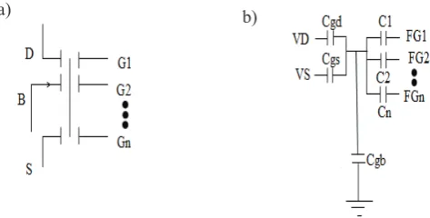
The equivalent circuit and symbol of n-inputs FGMOS are shown in Fig 1 (a) and (b) respectively. FGMOS is an altered version of the standard MOSFET in which it is fabricated by isolating the gate of conventional MOSFET electrically, therefore resulting zero resistive connections to its gate or more specific known as floating gate. Meanwhile, a number of secondary gates are electrically isolated from the floating gate and deposited above it [15].
Fig. 1. a) Symbol of n-inputs FGMOS; b) Equivalent schematic circuit of n-inputs FGMOS.
(1)
By utilising the charge of conservation law on the floating gate, the voltage at floating (VFG) can be
expressed below in (1) [2], [6], [8], [15]:
VFG = [C1V1 +C2V2+…+CnVn + CgdVd + CgsVs + CgbVb
+ Qfg]/ CT
In which, CT = C1+C2+…+Cn+Cgd+Cgs+Cgb and the
parasitic capacitances of floating gate with drain, source and bulk are represented by Cgd, Cgs and Cgb respectively.
The residual charge trapped at the floating gate during fabrication process is represented by Qfg which can be
eliminated by utilizing ultraviolet (UV) light, tunnel effect hot electron injection or forcing an initial condition with a switch [15],[16]
.
From the equation (1), it clearly show that FGMOS has no much differences compared to conventional MOSFET with a weighted sum of voltages applied onto its gate.
The weights are produced by the ratios between each input capacitance and the total capacitance at the floating gate node.
In consequences of the addition of the weights, in which is able to be realised without in need of using any additional circuitry, other than a number of capacitors. Therefore, the application of FGMOS can simplify certain circuit topologies and have a very positive significance on the circuit design in terms of area and power consumption.
Furthermore,
for the circuit designs that required to be operated by pushing the limits of the current technology, it is very crucial for the circuits to be designed in a simple manner [15].
Meanwhile the effective threshold voltage, Vth (eff) is
presented as below in (2) [2], [6], [8], [15]:
Vth (eff) = [VT– knVn] / k1 (2)
Where, k1 = C1 / CT, therefore, it can be seen that the
Vth, (eff) is able to be controlled by a suitable selection of
bias voltage, VT and ratios of capacitance. Hence,
making it possible to reduce the value of Vth(eff) that
contributes towards low voltage and programmable electronic devices [2].
3 Comparisons of FGMOS and NMOS
The ability of tuning and scaling down the threshold voltage enhances the gate delay time leading to a higher operation speed
.
Moreover, it is very crucial to reduce the threshold voltage when reducing the supply voltage.
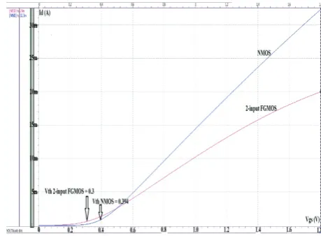
In Fig. 2, a proposed test circuit of FGMOS with 2 inputs and a conventional NMOS is presented
.
Fig. 2. Proposed test circuit of 2 inputs FGMOS and a conventional NMOS.
In the proposed test circuit, the transistors are using technology of 0.1µ with width of 20µ m and the supply voltage of 750mV. The output characteristics on comparative basis of drain current, Id versus source-gate
voltage, Vgs is simulated and shown in Fig. 3.
Fig. 3. Graph of drain current, Id versus source-gate voltage, Vgs.
It can be clearly seen in Fig. 2 that the threshold voltages, Vth produced by FGMOS is 0.3V which is
lower than the one that is produced by the conventional NMOS, 0.397V. Hence, it is proven that FGMOS is able to produce lower Vthin which can be done by controlling
This unique advantage owned by FGMOS allowing the programming of the signal levels individually on each device as required by the needs of the specific circuit design. In addition, by referring to equation (2), and the results from the simulated graph of Idversus Vgs,
we are likely be able to scale down the effective threshold voltage, make it zero. Consequently, this makes the FGMOS devices most suitable for application of circuits involving high degree of tunability or programmability. Therefore, for instance, the FGMOS devices are able to compensate for huge variations in performance due to mismatch [15]. The simulated graph of drain current, Id versus source-drain voltage, Vdsis
presented in Fig. 4.
Fig. 4. Graph of drain current, Id versus source-drain voltage, Vds.
4 FGMOS based inverter.
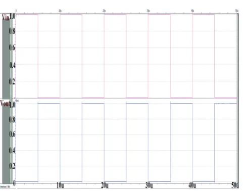
In order to observe whether FGMOS are compatible with MOSFET circuit design, an FGMOS device is placed in an inverter circuit which is shown in Fig. 5 and the resulted transient analysis is presented in Fig. 6.
Fig. 5.The FGMOS implementations in an inverter circuit.
Fig. 6.The transient analysis of inverter FGMOS
.
When both n-channel and p-channel MOSFETs are changed with 2 inputs n-channel and p-channel FGMOS with common floating gate
,
one of these transistors connected to a bias voltage and the other act as effective input,
causing the threshold voltage to remain the same.
In which,
the width and length of the channel for both n-channel and p-n-channel are similar to the conventional MOSFET implementation [15].
The switching threshold,Uinverter of a conventional CMOS inverter is shown in
equation (3) [15]
.
Uinverter ≈ [VDD - | VTp | + √(βn/ βp ) × VTn ] / (3)
[1 + √ (βn / βp)]
Where βn=µnCox (W/L)n and βp=µpCox (W/L)p are the
transconductance parameters of n and p channel FGMOS FGMOS [16]
.
Fig. 7 shows another FGMOS inverter circuit followed by a MOSFET inverter [15]
.
In the buffer circuit, the switching threshold value is not significant because it serves as the value of voltage at which the floating gate is not the input anymore since the floating gate and the output share the operating point (VFG = Vout).
In consequence,
it is more suitable to find thevalue of switching threshold at the effective input
.
The voltage is able to be obtained by combining the equation (1) and (3) resulting equation (4) [15].
V in(threshold) = [(CT/ Cin) – ( (Cgdn + Cgdp) / Cin)] × (4)
[(Vdd - | VTp| + √(βn /βp) × VTn) / ( 1+ √(βn / βp) ] -
Fig. 7. FGMOS inverter with two inputs followed by a MOSFET
.
In which, Cc and Cin are capacitances of FGMOS
connected to Vc and Vin respectively
.
By altering thevalue of Vc, from the equation (4)
,
it is shown that theswitching threshold of FGMOS inverter is able to be programmed
.
The objective of installing the second inverter is bifold, in which first it regenerates the digital levels and secondly
,
it helps to provide the comparisons of performances between FGMOS and MOS invertersThe results of this circuit is shown in Fig. 8
.
The output of the FGMOS inverter is represented by Vout1 inwhich is able to be achieved by sweeping Vin between 0V
to 2V and changing Vc in steps of 0.2V
.
Meanwhile, Voutis representing for the output of MOSFET inverter that connected in series with the FGMOS inverter and the aspect ratios are similar to the devices in FGMOS application
.
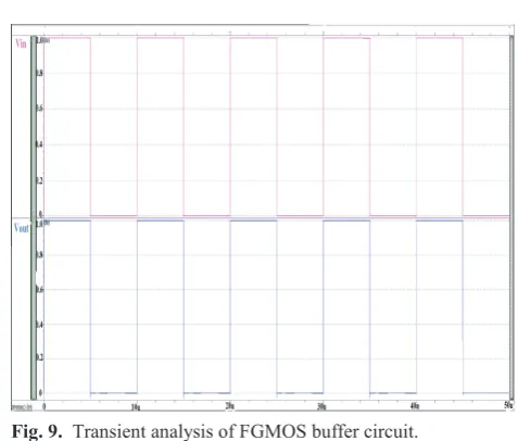
Fig. 9 shows the transient analysis of the buffer circuit proving that it can operate and producing result compatible with the CMOS buffer.Fig. 8. Input-output characteristic of FGMOS inverter followed by MOSFET inverter circuit
.
Fig. 9. Transient analysis of FGMOS buffer circuit.
From the simulated graph of input-output of FGMOS inverter in series with MOSFET inverter, it can be seen that by varying the Vc, the switching threshold is possible
to be programmed and eventually can be reduced. Therefore, FGMOS implementation is definitely suitable as an alternative technique in order to achieve low voltage and low power circuit design [17]
.
5 Conclusions
In this paper, we have studied the special advantage of FGMOS, in which it owns the ability to be programmed through the tuning of the threshold voltage. Meanwhile, through the comparison done between FGMOS and NMOS shows that the threshold voltage produced by FGMOS lowers than the conventional NMOS. Furthermore, the tunability of threshold voltage is initiated by the programmability of parameter k. This contributes towards achieving low voltage and low power circuit design. In addition, by changing the bias voltage of FGMOS in the inverter circuit, the inverter voltage transfer characteristics is able to be appropriately altered leading to the ability of changing the switching threshold, making it to be zero or even change its sign.
This research is supported by the Fundamental Research Scheme (FRGS) with Grant number 9003-00421 and sponsored by the Malaysian Ministry of Higher Education (MoHE).
References
3. B. Aggarwal, M. Gupta, and A. K. Gupta, Microelectronics J., 44, no. 3, 225–235 (2013) 4. A. Kumar, Analog Integr. Circuits Signal
Process., 80, no. 2, 305–314 (2014)
5. A. J. Lopez-Martin, J. M. Algueta, C. Garcia-Alberdi, L. Acosta, R. G. Carvajal, and J. Ramirez-Angulo, Microelectronics J., 44, no. 10, 920–929 (2013)
6. M. Gupta, R. Srivastava, and U. Singh,
Microelectronics J., 46, no. 2, 125–134 (2015) 7. M. B. K. Jamal, S. P. Chew, B. I. Khadijah, and
S. B. M. Noormiza, Adv. Mater. Res., 433–440, 4189–4193 (2012)
8. M.Moghavvemi and S. S. J. A. A., 2012 Int. Conf. Informatics, Electron. Vis., 588–592 (2012)
9. M. Gupta and R. Pandey, Microelectronics J., 42, no. 6, 903–912 (2011)
10. J. R. E. Hizon and E. Rodriguez-Villegas, Proc. - IEEE Int. Symp. Circuits Syst., no. 1, 2093–2096 (2014)
11. J. Lu et al., IEEE Journal of Solid-State Circuits, 50, no. 1, 270–281 (2015)
12. J. Lu and J. Holleman, Proc. - IEEE Int. Symp. Circuits Syst., 1600–1603 (2013)
13. R. Srivastava, M. Gupta, and U. Singh, Analog Integr. Circuits Signal Process., 78, no. 1, 245– 252 (2014)
14. R. Srivastava, M. Gupta, and U. Singh, Int. J. Electron., 102, no. 4, 563–581 (2015)
15. E. Rodriguez-Villegas, Low Power and Low Voltage Circuit Design with the FGMOS Transistor, 20, London, United Kingdom: The Institution of Engineering and Technology, London, United Kingdom (2006)
16. R. Gupta, R. Gupta, and S. Sharma, ELELIJ, 5, no. 2, 37–49 (2016)