ABSTRACT
TEMBE, CHINMAY SUNIL. Layout and Parasitic Extraction for FreePDK15™: An Open Source Predictive Process Design Kit for 15nm FinFET Devices. (Under the direction of Dr. W. Rhett Davis)
Over the years, the semiconductor industry has made rapid technological
advancements and developments and has adapted to countless new technologies,
methodologies and processes to save on valuable silicon area and achieve high speed and low
power utilization. Device scaling has been at the heart of the development of these
technologies as devices went from the micrometer range till few tens of nanometers.
Multi-gate device structures, commonly known as FinFETs have emerged as a favorable solution
for scaling beyond the 32 nm node with the large number of advantages it has, over planar
bulk CMOS technology. However, integrated circuit design with FinFETs is quite complex
and considerably different from that with older technologies. It is therefore essential for the
development of open source and easily available tools, kits and process flows for
introduction of the FinFET technology in university education
In this thesis, FinFET technology is introduced with a short discussion over its
advantages and complexities before a short introduction of physical layout verification
stages. A few possible lithography solutions for sub 32 nm technologies are mentioned and
based on these solutions and other research and development, a technology layer stack is
developed for the FreePDK15™, an open source process design kit for 15nm FinFET
technology. Layout extraction rules are developed and discussed to obtain successful LVS
assessed against these models. The thesis concludes with a brief description of shortcomings
and possible reasons and solutions for future research.
This thesis follows the research by Mr. Kirti Bhanushali, as the next steps in the
development of the FreePDK15™, an open source process design kit for 15nm FinFET
technology. The entire project aims at introducing FinFET based circuit design in universities
© Copyright 2015 Chinmay Sunil Tembe
Layout and Parasitic Extraction for FreePDK15™: An Open Source Predictive Process Design Kit for 15nm FinFET Devices
by
Chinmay Sunil Tembe
A thesis submitted to the Graduate Faculty of North Carolina State University
in partial fulfillment of the requirements for the degree of
Master of Science
Electrical Engineering
Raleigh, North Carolina
2015
APPROVED BY:
_______________________________ _______________________________
Dr. Brian A. Floyd Dr. Paul D. Franzon
_______________________________ Dr. W. Rhett Davis
DEDICATION
All of my efforts are dedicated to my mother Mrs. Seema S. Tembe, my father Mr. Sunil D.
Tembe, my family and my friends who have supported me throughout my education and
BIOGRAPHY
Chinmay Sunil Tembe has completed his Bachelor’s degree in Electronics and
Telecommunication Engineering from the University of Mumbai in 2013. In Fall 2013, he
joined North Carolina State University for his Master of Science degree in Electrical
ACKNOWLEDGMENTS
I would like to thank Dr. W. Rhett Davis for providing me with the opportunity to work on
this project, and for all his guidance throughout the duration of this thesis. His invaluable
inputs and advice have made it possible for me to shape and direct my efforts into the
completion of this thesis.
I would like to express my gratitude to the teams at Mentor Graphics Corporation and
NanGate who have supported this project and have provided various aids and tools in the
completion of the same. I also would like to thank Mr. Kirti Bhanushali for his able advice
and guidance during various stages of this project.
I also would like to thank the entire staff of the Department of Electrical and Computer
Engineering at North Carolina State University for all their help and also to the staff of North
Carolina State University Libraries for providing access to all the required resources and
research papers online.
I would like to thank and appreciate the support and love that the families of Atkikar,
Bhagwat, Chitale, Huprikar, Joshi, Khambete, Modagi, More, Phadke, Rajwade, Salvi,
Sansare, Shetye and Tembe have shown for as long as I can remember.
I would like to offer my special thanks to Priyanka Shankaran for all her support for the past
two years and for giving valuable inputs and feedback in completing this thesis.
And finally I would like to express deep gratitude to Shashank Phalke, Chinmay Kulkarni,
Harsh Sarda, Parth Dhanani, Kshama Satam, Shreya Joshi, Gaurav Pande, Chinmay Gore,
TABLE OF CONTENTS
LIST OF TABLES ... vii
LIST OF FIGURES ... viii
1. Motivation ... 1
1.1. Outline ... 2
2. FinFETs – Solution beyond 22nm ... 4
2.1. FinFETs ... 5
2.2. Layout Verification ... 7
3. FreePDK15™ Technology Stack ... 10
3.1. FreePDK15™ Layers ... 13
3.1.1. BEOL Layers ... 15
3.1.2. MOL Layers ... 19
3.1.3. FEOL Layers ... 20
3.1.4. Other layers/Masks ... 21
4. Layout Extraction ... 22
4.1. LVS Rule File ... 22
4.2. Layout Rules for FEOL and MOL Layers ... 27
4.2.1. Well contacts... 31
4.3. BEOL Layers ... 41
4.3.1. Metal Stitching ... 42
5. Parasitic Extraction ... 47
5.1. The .mipt file ... 50
5.1.1. FEOL and MOL Stack ... 52
5.1.2. BEOL Stack ... 55
5.2. Parasitic Extraction for two input NAND Gate ... 58
5.3. Validation ... 59
5.4. Parasitic Capacitance ... 66
5.4.1. Parallel Plate Capacitance Validation ... 66
5.4.2. Fringing Capacitance Validation... 72
5.4.3. Coupled Capacitance Validation ... 79
5.4.4. Additional Validations ... 82
5.5. Parasitic Resistance ... 84
5.6. HSPICE Simulations for NFinFET ... 89
5.7. HSPICE Simulations for Inverter Chains ... 91
5.8. Avenues for Errors ... 94
LIST OF TABLES
LIST OF FIGURES
Figure 1: a) Traditional Planar Bulk Transistor [7] b) 22nm FinFET [7] ... 5
Figure 2: a) Sources of Parasitic Capacitances in FinFETs [8] b) Multi-fin FinFET [7] ... 6
Figure 3: Proposed Lithography methods a) Immersion Lithography b) Double Patterning .... 10
Figure 4: Metal Layer Widths [5] ... 12
Figure 5: BEOL Metal Layer Stack ... 17
Figure 6: FEOL and MOL Layer Stack ... 19
Figure 7: NMOSFET in FreePDK45™ ... 27
Figure 8: NFinFET (without body contact) in FreePDK15™ ... 29
Figure 9: Common well contact for two inverters ... 32
Figure 10: Common well contact for two inverters - only FEOL layers shown ... 33
Figure 11: Two inverter circuits with separate well contacts (generates LVS errors) ... 34
Figure 12: Two inverter circuits with separate well contacts - only FEOL layers shown (generates LVS errors) ... 34
Figure 13: Solution for creating multiple well contacts ... 35
Figure 14: NFinFET Layout ... 36
Figure 15: PFinFET Layout ... 36
Figure 16: Gate Cut Mask (GATEC) example ... 38
Figure 17: Gate Cut Mask (GATEC) example - only FEOL layers shown ... 39
Figure 18: MOL layer connections ... 40
Figure 19: Metal Stitching example ... 43
Figure 20: Metal Stitching example a) Problem b) Solution ... 44
Figure 23: Process Flow for parasitic extraction using Mentor Graphics' Calibre xCalibrate
and Calibre xRC ... 49
Figure 24: FEOL and MOL layer stacks in Mentor Graphics' Stack Viewer a) Stack with poly and GIL b) Stack with AIL1 and AIL2 ... 54
Figure 25: BEOL layer stack in Mentor Graphics' Stack Viewer a) Global metal layers b) Semi-Global metal layers c) Intermediate metal layers and layer M1 ... 57
Figure 26: Schematic with various parasitics in an NFinFET Layout (without coupling capacitances) ... 64
Figure 27: Parallel plate capacitance ... 67
Figure 28: Layout modification for parallel plate approximation ... 68
Figure 29: Parallel plate capacitor ... 69
Figure 30: Layout modification for fringing capacitance approximation ... 73
Figure 31: Total capacitance approximation [23] ... 74
Figure 32: Layout modification for coupled capacitance ... 80
Figure 33: Layouts for resistance validations a) NFinFET Layout b) NFinFET layout with increased length for Drain terminal metal layer ... 85
Figure 34: Propagation delay calculation for NFinFET - Basic circuit ... 90
Figure 35: Propagation delay calculation for NFinFET - circuit with areas and perimeters of drain and source ... 90
Figure 36: Propagation delay calculation for NFinFET - with all extracted parasitics ... 91
Figure 37: Chain of inverters (FO1) - well, implant layers not shown ... 92
Figure 38: Chain of inverters (FO4) - well, implant layers not shown ... 92
Figure 39: Propagation delay for inverter chain (FO1) - with all extracted parasitics ... 93
1. Motivation
FinFET Technology might well be the epicenter of the all the technological progress
the semiconductor industry might see in the near future. FinFETs offer all the benefits of
scalability and with lesser problems that traditional bulk CMOS technology faces. It may
well be the cornerstone for years of research and development to come. The semiconductor
industry is already adapting to this new technology which is quite unlike its predecessors and
has already taken steps to develop new methodologies, design patterns to best suit further
development using FinFETs. Major foundries like GlobalFoundries and Intel have already
begun manufacturing FinFETs for 22nm or lower technologies and also have started
providing design platforms and kits for their customers [1].
Universities and academia, however, have reluctantly remained behind owing to lack
of resources, large number of patents and intellectual properties and the colossal amount of
money required for proper licensing of tools required to delve more into this area. There is a
dire need for cheaper alternatives, open source tools in order to get a foothold into this new
technology. The BSIM group, of University of California, Berkeley, has developed a
compact model [2] for multi-gate FETs and has already provided a great depth of insight for
circuit simulations at these technology nodes. Currently, there are no public models, kits or
rules available for physical layout verification for FinFETs beyond 22nm.
FreePDK15™ [3] is an open source process design kit for design with FinFETs. The
project aims at providing an opportunity for university students to gain good understanding
of the complexities involved in integrated circuit design, especially with FinFETs at
designs which are important stages of the physical verification flow before fabrication.
Various techniques like multiple patterning, metal stitching are taken into consideration before developing the technology stack for FreePDK15™ before laying out the various
layout and parasitic extraction rules. A process flow is developed for physical verification
which encourages development of similar process development kits for different technologies
and applications. One of the motives is to develop FreePDK15™ in a way, so that it can
serve as a reference for development of other resources, tools and kits which could be used
by the academia to better understand and explore designing with sub 22nm technologies.
1.1. Outline
This thesis briefly explores the proposed lithography methodologies for sub-22 nm
technologies, before delving into device and parasitic extraction from layouts and their
verification. There is an attempt to develop a physical design verification process flow, to let
the students and researchers gain a thorough understanding of physical design and also
enable them to develop their own design kits for sub-22nm technology based integrated
circuits.
The thesis begins with a brief introduction to FinFET technology and the challenges it
faces especially from the point of view of parasitics. In chapter 3, A few lithography methods
proposed for the sub-22nm technology are reviewed and the technology stack for FreePDK15™ and its development are discussed. Chapter 4 talks about layout extraction and
development of rule file for Layout-Versus-Schematic (LVS) checks for logic development.
to validate the results of a parasitic extraction run. Various results for the parasitic extraction
runs on a few simple circuits are presented and a few of them are compared with the
International Technology Roadmap for Semiconductors predictions from the 2011 roadmap
for the 2016 node, and the chapter concludes with the discussion of possible avenues of
errors in the extraction results. The last chapter summarizes the thesis and gives an insight
2. FinFETs – Solution beyond 22nm
The Integrated Circuit technology has, over the years, developed with an exponential
growth rate. From the initial modest beginnings, the device size has gone down to a small
fraction of a nanometer, and still continues to decrease. To meet the ever-growing consumer
demands, the semiconductor industry has adapted over the years with several innovations and
novel design methodologies to provide astonishing speed, accuracy and a wide variety of
functionality. To tackle the problem of ever-increasing power issues, several low power
solutions were found and the industry continued to march on.
Despite several problems that arise, device scaling has continued at a steady pace for the industry to, more often than not, meet the “Moore’s Law”. The planar-bulk CMOS
technology which has been a constant for quite some time until the 32 nm technology node,
has now run into several issues. According to the International Technology Roadmap for
Semiconductors (ITRS) 2011 Executive Summary, the conventional path of scaling, which
was accomplished by reducing the gate dielectric thickness, reducing the gate length and
increasing the channel doping, might no longer meet the application requirements set by
performance and power consumption [4]. At such smaller device dimensions, short channel
effects come into play, which degrade the device performance. Second-order effects like
channel-length modulation, Drain-Induced Barrier Lowering (DIBL), subthreshold leakage
and others cause severe problems for short channel devices [5]. The issues and the effects
they have on device performance are described at length in [5]. Some solutions have been
for the required performance and power requirements. ITRS 2011 [4] suggests two possible
implementations which could be adopted for devices beyond 22nm node – Fully Depleted
silicon-on-insulator (SOI) and multi-gate (MG) structures. While fully-depleted SOI are
suitable for sub 22nm design, many foundries, notably Intel, are researching and developing
multi-gate structures.
2.1. FinFETs
Multi-gate structures are commonly implemented and termed as FinFETs owing to
the narrow Si fin that is formed which is overlapped by the gate. Two implementations of
multi-gate structures is possible – SOI FinFET and bulk FinFET. [6] compare performances
of SOI and bulk FinFETs for sub-threshold and on-state performance. Both structures have
comparable performances in both sub-threshold and on-state regions, but fabrication of SOI
devices faces some issues like higher wafer cost and higher wafer defect density.
FinFETs derive its name from its structure, which has a small Si fin-like structure,
surrounded on three sides by gate layer. This 3D structure is what gives FinFETs, most of its
superior qualities over planar bulk MOSFETs. The very obvious advantage is the density that
can be achieved using FinFETs as compared to planar bulk devices. The ratio of areas of a
15nm FinFET to that of a 45nm planar MOSFET is approximately 1/6 [5]. Moreover, the
gate which covers the fin on three sides provides much better gate-control on the channel,
which leads to reduction in the short channel effects. The Si fin which forms the channel is
undoped which means that FinFETs have no Random Dopant Fluctuation issues that
traditional planar devices face. Also, they have reduced gate leakage, which is one of the
most attractive reasons to use FinFETs beyond 22 nm.
Figure 2: a) Sources of Parasitic Capacitances in FinFETs [8] b) Multi-fin FinFET [7]
These advantages certainly give FinFETs the edge over other competitive structures
have analyzed the parasitic capacitance due to the complex 3D structure of the FinFETs
especially the Multi-fin structure shown in Figure 2b) and have developed RC models [10]
for the same. Figure 2a) gives a good idea of the large number of parasitics that are
introduced because of the 3D structure of the FinFETs. The gate to S/D capacitance
dominates the total gate capacitance in a FinFET [9], especially for multi-fin devices.
Moreover, lithography methodologies for fabricating FinFETs are slightly more complex
than traditional planar devices. Spacer Lithography and Multiple patterning are some of the
techniques proposed and successfully experimented on, using 193i water immersion
lithography which is currently being used for devices until the 32 nm node. The results have
been satisfying and the industry has adapted these techniques until research on EUV
lithography produces some ground breaking results. Many new layout coloring algorithms
[11] [12] have been proposed to utilize multiple patterning.
Thus, despite the large number of advantages that FinFETs have to offer, designing
and fabricating these devices is quite complex and takes a great deal of effort and
understanding. Several modifications have to be made in circuit design as well as the
physical layout design and verification stages. [5] describes the design rule considerations for
the 15nm FinFET design, while this thesis describes the layout rules and extraction of
parasitics from layouts.
2.2. Layout Verification
The final stages of design before fabrication, requires creation and verification of a
physical layout design of the circuit. A layout is simply a mesh of shapes of different layers
checked for violations pertaining to the design rules for the technology used for fabrication
and also for correctness of the layout, meaning whether the layout represents the desired
circuit correctly and whether connectivity is passed as desired. There is also a parasitic
extraction run where, parasitics are extracted from the layout and added to the so-far ideal
circuit netlist. These parasitic extraction runs give a good idea of the amount of non-idealities
that might be added once the chip is fabricated to a physical form. The simulation of the
netlist with the parasitics serves as a good sanity check of how the circuit functionality is
affected due to parasitics and if modifications are required to obtain desired functionality.
This is followed by adding process variations to the layout and checking whether the layout
would generate violations under the worst of lithography process variations.
The semiconductor industry relies on Electronic Design Automation (EDA) tools to
forecast all these issues before the design is sent to the foundries for fabrication. DRC
Checks are used for checking design rule violations while a Layout Versus Schematic (LVS)
comparison check is made to verify proper connectivity. This thesis makes use of EDA tools
developed by Mentor Graphics. The tools used are Calibre nmDRC [5], Calibre nmLVS,
Calibre xCalibrate, Calibre xRC.
1. Calibre nmDRC is an EDA tool for checking design rule violations in a layout. This
tool has been used widely in [5] for developing design-rules for FreePDK15™.
2. Calibre nmLVS is used to perform Layout versus Schematic comparisons. This is a
3. Calibre xCalibrate is a 3D field solver tool which develops parasitics rule files based
on the technology file that is input and performing calculations based on Maxwell’s
equations. It develops the rule files that are required for Calibre xRC [13].
4. Calibre xRC generates a netlist of the layout while calculating and adding the
3. FreePDK15™ Technology Stack
Technology has scaled steadily over the years with new challenges with every new
technology node. Innovative solutions have been suggested and implemented to tackle these
problems and the design methodologies and lithography steps have adapted to the
requirements of the node. As the critical dimension of the devices went down, the
lithography process transitioned from 248nm to 193 nm. Further modifications were the
water immersion technology with the 193nm light source. The water immersion lithography
with 193nm ArF laser has given good yield and manufacturability until the 32nm node.
Further scaling puts a lot of constraints on this technology. As a result, for patterning below
32nm technology, three possible solutions have been proposed.
Figure 3: Proposed Lithography methods a) Immersion Lithography b) Double Patterning
The first solution is to use 193 nm lithography techniques, with high refractive index
immersion lithography). However, this method requires considerable development in
material science for new materials with such high refractive indices and high transparencies
and it might still be some time before this method could become feasible for patterning
sub-32 nm devices [14]. The second method is the use of Extreme Ultra-Violet (EUV) light
sources. However, EUV sources currently available are unreliable and much more costly for
researching sub-32nm nodes [15]. The third option is multiple patterning. Multiple patterning
aims at relaxing the minimum pitch required for lithography by dividing the design into two
masks. This methodology has been proven to be successful and many methods have been
proposed to implement double patterning using current lithography processes. The easiest
one is Litho-Etch-Litho-Etch (LELE) which basically builds on double exposure for the two
masks, one after another with the help of a hard-mask which protects the pattern created by
the first mask. Another method proposed includes a ‘freezing’ step to preserve the patterns
printed in the first step – Litho-Freeze-Litho-Etch (LFLE) [15]. The third process known as ‘Self-Aligned Spacer Double Patterning (SADP)’ has so far provided promising results.
SADP avoids overlay errors as patterns are obtained from single exposure while the doubling
achieved by formation of spacers and bottom hard masks [14].
According to the International Technology Roadmap for Semiconductors, total wire
lengths within an SoC has increased by 60% in the past five years to more than 3km/cm2
[16]. That is a huge length of wire and it will have a large amount of parasitics associated
with it. Moreover, with the scaling of devices, as the thickness of the wire has gone down,
the wire resistance and the contact resistance has gone up. This increase in resistance
connecting the Front-End-of-Line (FEOL) layers to the Back-End-of-Line (BEOL) metal
hierarchy via contacts/vias, new layers known as Middle-of-Line (MOL) layers are
introduced which connect to underlying layers (diffusion, poly etc.) without any
vias/contacts. This greatly reduces the parasitics associated with the large connections to the
metal layers. These layers also provide a way to have denser layouts by making device
connections using these layers.
ITRS 2011 roadmap [4] has predicted that for a gate length of 15.34 nm, the
minimum number of metal layers in the interconnect stack must be 13. The metal layer stack
follows the standard ASIC design methodology architecture [4] [5]. There are four kinds of
metal layers – metal1, intermediate, semi-global and global.
3.1. FreePDK15™ Layers
The layer stack for the FreePDK15™ 15nm technology has been developed by
considering all of the things said before. Table 1 gives all the layer names and a short
description.
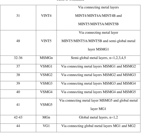
Table 1: FreePDK15™ Layer Description
GDSII Layer Number Layer Name Description
0 NW N-Well, P-Well assumed to be where NW is not found
1 ACT Active Area for fin definition
2 VTH High Threshold adjust mask
3 VTL Low Threshold adjust mask
4 THKOX Thick-Oxide adjust mask
5 NIM N-Implant
6 PIM P-Implant
7 GATEA Gate metal, Color A
8 GATEB Gate metal, Color B
9 GATEAB Gate metal, single color
10 GATEC Gate metal cut mask
11 AIL1 Active-Interconnect-Layer, level 1
Table 1: Continued
13 GIL Gate-Interconnect-Layer
14 V0
Via zero, connecting interconnect layers to metal layer
M1/M1A/M1B
15 M1A First metal layer, color A
16 M1B First metal layer, color B
49 M1 First metal layer, single color
17 V1
Via connecting metal layers M1/M1A/M1B and
MINT1/MINT1A/MINT1B
18-22 MINTnA Intermediate metal layers n=1,2,3,4,5, Color A
23-27 MINTnB Intermediate metal layers n=1,2,3,4,5, Color B
50-54 MINTn Intermediate metal layers n=1,2,3,4,5, single color
28 VINT1
Via connecting metal layers
MINT1/MINT1A/MINT1B and
MINT2/MINT2A/MINT2B
29 VINT2
Via connecting metal layers
MINT2/MINT2A/MINT2B and
MINT3/MINT3A/MINT3B
30 VINT3
Via connecting metal layers
MINT3/MINT3A/MINT3B and
Table 1: Continued
31 VINT4
Via connecting metal layers
MINT4/MINT4A/MINT4B and
MINT5/MINT5A/MINT5B
48 VINT5
Via connecting metal layer
MINT5/MINT5A/MINT5B and semi-global metal
layer MSMG1
32-36 MSMGn Semi-global metal layers, n=1,2,3,4,5
37 VSMG1 Via connecting metal layers MSMG1 and MSMG2
38 VSMG2 Via connecting metal layers MSMG2 and MSMG3
39 VSMG3 Via connecting metal layers MSMG3 and MSMG4
40 VSMG4 Via connecting metal layers MSMG4 and MSMG5
41 VSMG5
Via connecting metal layer MSMG5 and global metal
layer MG1
42-43 MGn Global metal layers, n=1,2
44 VG1 Via connecting global metal layers MG1 and MG2
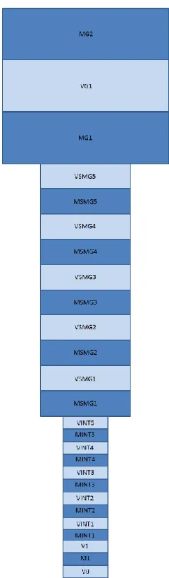
3.1.1. BEOL Layers
According to ITRS 2011 roadmap interconnect tables, for the 2016 node the metal
hierarchy has 13 metal layers. The number of metals in each type – intermediate, semi-global
extent semi-global as well, are huge and bulky layers with large dimensions and not
necessarily the best for creating a highly compact layout design. Meanwhile, intermediate
and metal1 layers, which have same dimensions, can be used for denser layouts, but have
much higher wire resistance and parasitic capacitances owing to their smaller thicknesses and
smaller critical spacing. Hence, they contribute in a large way towards the parasitics of the
circuit. Similar, other relations could be found and a trade-off could be made and an
appropriate metal layer stack could be decided upon.
For FreePDK15™, a general layer stack is assumed without worrying much about the
delays and layout density.
metal1 is the lowest layer. Two global metal layers are used (for power and ground
rails). The remaining 10 layers are divided equally into 5 intermediate and 5 semi-global
metal layers. That gives a total of 13 metal layers. Each pair of metal layers has a via
between them for electrical connection. A via takes the thickness and dimensions of the
lower metal layer.
Tetraethyl orthosilicate (TEOS) is assumed as the dielectric surrounding the metal
layers while copper is assumed as the conducting material for the metal layers. The minimum
width of the metal layer – metal1 is assumed to be 28nm. Intermediate metal layers have the
same dimensions as metal1. Semi-global metal dimensions are twice that of metal1 and
hence the minimum width for semi-global metal layers is 56nm. Global metal layers are four
times the dimensions of metal1. Hence, the minimum width for Global metal layers is
Since SADP (or some other technique) is used for multiple patterning, all the metal
layers that have critical dimensions smaller than 32nm are subject to multiple patterning.
Thus, we have the following metal layer stack and metal layers.
1. M1A, M1B – Multiple-patterning layers of metal1 type. First layer of interconnect
metal. They are generally used for connecting MOL layers to metal layer stack.
2. M1 – Single layer for metal1 layers, to be processed later. This layer is useful for
simplifying layouts. M1 can be used instead of M1A and M1B while creating layouts.
Layout coloring is generally a later stage when the complete layout is analyzed for the
best possible coloring scheme.
3. MINTnA, MINTnB – (n=1,2,3,4,5) Multiple patterning layers of intermediate metal
type. They are generally used for connecting various devices together.
4. MINTn – (n=1,2,3,4,5) Single layer for intermediate metal layers, to be processed
later. This layer is useful for simplifying layouts. MINTn can be used instead of
MINTnA and MINTnB while creating layouts. Layout coloring is generally a later
stage when the complete layout is analyzed for the best possible coloring scheme.
5. MSMGn - (n=1,2,3,4,5) Semi-global metal layers. They are generally used for
connecting various sub-circuits/circuits together. They are much larger than the
intermediate metal layers and contribute largely to parasitics.
6. MGn – (n=1,2) Global metal layers. They are generally used for connecting global
Figure 6: FEOL and MOL Layer Stack
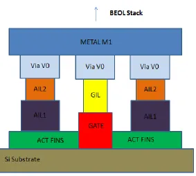
3.1.2. MOL Layers
Middle-of-Line layers are used as local interconnects passing connectivity from fins
(ACT) and poly (GATEA, GATEB, GATEAB) layers to metal layer stack. [17] observed
that for 14nm Bulk FinFET devices, introduction of IM1 (local interconnect1, here, AIL1)
strongly reduces the spread on standard cell performance. Also, if Self Aligned IM1 (local
interconnect1, here, AIL1) is used along with Double Patterning LELE GATE layers,
(AIL2 can also be connected to gate), while double patterning GATEA, GATEB are used for
device gate definitions.
The MOL layers are as follows-
1. Active Interconnect Layer 2 (AIL2) – AIL2 layer passes connectivity from lower
local interconnect layers onto the BEOL metal hierarchy through via V0.
2. Active Interconnect Layer 1 (AIL1) – AIL1 connects fins (ACT layer) of devices to
AIL2 layer.
3. Gate Interconnect Layer (GIL) – GIL can either connect to AIL2 to pass on the poly
(GATEA, GATEB, GATEAB connectivity) or can pass the connectivity to the BEOL
metal layer stack through via V0.
3.1.3. FEOL Layers
Multiple patterning is assumed for gate layers as well so as to get a uniform pattern of
connected and dummy gates at half the pitch spacing. The FEOL layers are as follows-
1. GATEA, GATEB – Multiple-patterning layers for gate layer (or poly). They form the
gate pin and are passed as a layer for device recognition.
2. GATEAB – Single layer for GATEA, GATEB layers, to be processed later.
3. GATEC – Gate cut layer. This layer is actually kind of a negative mask. It is used to
sever connectivity between gate layers that are continuous. It is very convenient to
form long GATEA/GATEB/GATEAB shapes and the create multiple individual gate
shapes by using a grid of GATEC layers, rather than patterning multiple gate shapes
SiN is assumed as the dielectric surrounding all FEOL and MOL layers except AIL2
which has Silicon dioxide. For GIL, the area common to AIL1 has SiN while the area
common to AIL2 has Silicon dioxide.
3.1.4. Other layers/Masks
These layers are more of patterning masks rather than layers. They are defined as layers because the Mentor Graphics’ Calibre Standard Verification Rule Format requires all
layer operands to be layers. And these layers are used to derive various layers required for
pin or device recognition.
1. NW – nwell Mask. pwell is assumed wherever Nwell is not present.
2. NIM – N-Implant Mask
3. PIM – P-Implant Mask
4. VTH – High Threshold adjust mask
5. VTL – Low Threshold adjust mask
4. Layout Extraction
‘Layout Extraction’ can be thought of as a collective term for device recognition and
connectivity extraction from an array of overlapping geometrical shapes of different layers in
the technology stack. The geometrical design is the physical implementation of a circuit/chip
and the extraction step must be perfect to derive a meaningful circuit netlist from the
geometrical design. This extracted netlist is then compared with the netlist of the circuit/chip
which is to be designed. This is called a Layout Versus Schematic (LVS) Check. The layout
extraction combined with the LVS comparison step, forms one of the most crucial steps in
physical verification. Not only does the extraction must be exact, a thorough LVS
comparison is required to check whether the geometrical design or the layout is an exact
physical representation of the desired circuit. With the scaling of devices and new
technological nodes, more and more layers are added to the layer stack and that adds to the
complexity of creating a perfectly matching layout. LVS comparison is a way to make sure
that all the desired devices are represented correctly in the layout and that the connectivity is
established in the layout for every net in the schematic.
4.1. LVS Rule File
Layout Extraction and LVS Comparison are generally performed together sequentially by the same tool. Mentor Graphics’ Calibre nmLVS extracts a netlist from the
layout, generally a .gds file (if Calibre GUI is used a .calibre.db file is created which is same
as that of a .gds file). The .gds file contains all the dimensional information about the various
information apart from other Rule-Check statements. Then, based on the device definitions
and connectivity information, the tool searches the layout for a shape, or a group of shapes
that matches the device and layer description in the rule file and generates a netlist based on
the devices and connectivity extracted from the layout. This netlist, which corresponds with
the layout, is compared with the source netlist (the schematic netlist), and the results are
printed out. The comparison is on the basis of number of nets, devices and pins/ports in the
schematic and the layout netlists. If a layout passes the LVS comparison then it perfectly
represents the schematic and can be sent to the next step of verification. Assuming ideal
fabrication results, a layout that passes LVS comparison, when fabricated would function as
expected.
The rule file is thus, the most crucial resource in the complete layout extraction and
comparison step. The rule file must contain all the layer definitions, layer connectivity information, definitions for all possible devices. According to Mentor Graphics’ Standard
Verification Rule Format Manual [18], the general rule file contains the following statements
1. Layer Assignment Statements
2. Global Layer Definitions
3. Comments
4. Include Statements
5. Rule Check Statements {
Local Layer Definitions
Layer Operations
}
6. Specification Statements
7. Connectivity Extraction Operations
8. Parasitic Extraction Statements
9. Device Recognition Operations
10. Conditionals
11. Macros
12. Runtime TVF Functions
Although, it is not mandatory for all of these statements to be included in a rule file,
most of them are, in a way, necessary to have a successful LVS comparison run.
Layer Assignments and Definitions include defining layers in the layer stack to a
calibrated layer list while also defining various derived layers to be used for device
recognition. Layer operations are used to manipulate layer data. There are different types of
layer operations, with the main basis of qualification being the way connectivity is passed to
layers in the operation. Comments can be used as and when required. Include Statements are
used to include various other rule files, to have a better division of rules. This also helps
when the rule file size grows as more and more features are added to it. Rule-Check
statements specify layer operations whose resulting derived layers are placed into the results
database when the statement is executed. Specification statements set the environment for the
layout extraction runs. Connectivity, Device and Parasitic Operations are special operations
file. MACROs are like functions in programming languages. They are defined once and
invoked whenever required. Runtime functions require a TVF function to define operations
to perform when the tool is running.
As mentioned before, not all of these are required in a rule check statements. The rule
file for LVS Check for FreePDK15™ uses only a subset of these statements viz. Layer
Assignment Statements, Comments, Include Statements, Specification Statements,
Connectivity Extraction Operations, Device Recognition Operations and MACROs. The
Parasitic Extraction Statements are used in the xRC rule file (discussed in Chapter 5). The
use of these statements in the rule file for FreePDK15™ is described next.
Note: The rule files for LVS and Parasitic Extraction are kept separate for convenience and taking into consideration the time required for each respective run.
The Comments, Include and Specification statements are used for the same purposes
as described previously. Layer Assignment statements are used to define layers which are in
the Layer Stack and also to define new derived layers using layer operations. These derived
layers are used to identify possible shapes in the layout and those can be used to pass
connectivity or define devices. Connectivity Extraction statements are ‘connect’ and ‘sconnect’. ‘connect’ is the most commonly used statement for connecting two layers directly
– for the local interconnect layers (MOL) or indirectly with a via – for the metal hierarchy.
‘sconnect’ is used only in a couple of places for derived layers because all layer operations
are performed before connectivity is established [18]. Derived layers do not get the
connectivity because when the layer operation for a derived layer is executed, none of the
make any difference in LVS comparison. But if ‘connect’ statements are used instead of
‘sconnect’ for derived layers used in device recognition, Parasitic Extraction run throws out
the warning – “ derived_layer is not mapped to a calibrated layer”.
FreePDK15™ has been developed for FET designs only (no resistances and
capacitances are separately defined as devices). Hence, the only PFinFETs and NFinFETs are
the devices defined and recognized in a layout. However, modifications of N and P FinFETs
are available with low threshold, high threshold and with thick-oxide corrections. The Device
Recognition statements are used and the corresponding derived/original layers are passed as
pin layers to define pins on those layers. Connectivity is first established in the layout and
then the device statements are executed. All possible shapes that match the device statement
description are subject to a further recognition step. The Device statement passes a device
seed layer, various pin layers and optional auxiliary layers. The device layer is scanned for
all possible seed shapes, while the pin layers and auxiliary layers (if any) are also scanned.
The auxiliary layers are scanned, to find which of the seed shapes touch (overlap or abut), at
least one of the shapes on the auxiliary layer. The pin layers are scanned to form initial pins
based on whether the seed shapes touch the pin layers. Once this is done, device shapes that
passed the auxiliary layer test and have exact number of pins from the initial pins formed, are
considered as an exact match for a particular device [19].
MACROs are like functions in a programming language; they are defined once and
are invoked whenever required. One MACRO is used in the LVS rule file, to assign
4.2. Layout Rules for FEOL and MOL Layers
As stated previously, FreePDK15™ has been developed for FET designs only (no
resistances and capacitances are separately defined as devices). The only devices that are
defined in the rule file are NFinFETs and PFinFETs. The technology layer stack however,
provides three masks – Low Threshold Adjust Mask, High Threshold Adjust Mask and
Oxide-Thickness Adjust Mask and hence 6 other devices are defined two (corresponding pfet
and nfet) for each mask viz. NFinFET_VTL, PFinFET_VTL, NFinFET_VTH,
PFinFET_VTH, NFinFET_THKOX, PFinFET_THKOX.
Designing FETs using traditional bulk technology is considerably different from
designing FinFETs. To get a better idea of the difference, a layout of a minimum-sized
NMOSFET designed in the 45nm FreePDK45™ technology is compared with a layout of a
minimum-sized NFinFET designed in the 15nm FreePDK15™ technology.
A bulk MOSFET layout is defined by the width and length parameters, which are
both scalable with the minimum size being the technology pitch. For instance, for 45nm
technology, the minimum width and length of the MOSFET are 45nm but depending on the
requirements of the circuit, both of these can be scaled up to the required values. The width
of the Active area determines the width of the transistor while the width of the Poly shape
intersecting the Active area is the length. Dense 45nm layouts are easily printed by the
193nm water immersion photolithography process. The FEOL layers are connected to the
metal hierarchy BEOL layers directly with the help of vias/contacts. Also, the drain and
source areas and perimeters required for the junction capacitance calculation is pretty simple
for bulk CMOS devices.
𝐴𝐷= 𝐴𝑆 = 𝑊 × 𝐿𝐷/𝑆 (4.1)
Figure 8: NFinFET (without body contact) in FreePDK15™
Note: The layouts used for various simulations in this thesis are based on the FreePDK15 Open Cell Library developed by NanGate [20]. In most of these layouts, the basic transistor
structure is drawn as per FreePDK15 Open Cell Library by NanGate. However, various
modifications are made as per the requirement. The metal widths are kept consistent with the
design rules developed in [5].
A FinFET layout on the other hand is much more complicated than the one for its
bulk CMOS counterpart. The width of the Active area for a FinFET is not the actual width of
the device. The actual width 𝑊𝑒𝑓𝑓, of a FinFET device is depended on the fin width 𝑊𝑓𝑖𝑛,
and fin height 𝐻𝑓𝑖𝑛, parameters. It is given by
Moreover, FinFETs are characterized by the gate length and number of fins (and also
sometimes number of fingers). The gate-length is, just like that of a NMOSFET, still the
channel length. However, the gate-length is not scalable according to the requirements. The
only allowed gate lengths are 14nm, 16nm, 20nm. Multiple finger FinFETs are used to
increase the gate lengths. Similarly, width of a FinFET which is given by equation (4.3) is
hence not scalable either. It is dependent on the number of fins that a FinFET has. The width
of the Active area can be 48nm at a minimum and only 40nm increments are allowed. Thus,
both length and width scaling is discrete. The FEOL layers are separated by the BEOL layers
by the MOL layers. The FEOL layers are connected to the MOL layers – AIL1, AIL2 for
Fins and GIL, AIL2 for Gate connections. These local interconnects are connected to the
metal hierarchy by vias/contacts. Also, fabricating FinFETs with 193nm water immersion
process is not possible which is why we have to use multiple patterning layers for a compact
layout. Also dummy gates are added to complete the layout.
Although the formula for source and drain areas are same for single-fingered and
multi-fingered devices, there are two different formulae for the drain and source perimeters.
The sidewall contribution for a single-fingered device (or no device in the horizontal
direction) is more than that for a multi-fingered device. This is because for the multi-fingered
device, one of the edges is common to two fins and does not contribute to the sidewall
capacitance. The areas and perimeters of drain and source are as follows.
For one finger devices,
𝑃𝐷𝐸𝐽 = 2 × 𝐿𝑓𝑖𝑛𝐷× 𝑛𝑓𝑖𝑛+ 𝑊𝑓𝑖𝑛× 𝑛𝑓𝑖𝑛 (4.6)
𝑃𝑆𝐸𝐽 = 2 × 𝐿𝑓𝑖𝑛𝑆× 𝑛𝑓𝑖𝑛+ 𝑊𝑓𝑖𝑛× 𝑛𝑓𝑖𝑛 (4.7)
However, the values change for a multi-fingered device, as the length has to be
adjusted as well. ADEJ and ASEJ formulae remain the same but with the reduced drain
and/or source length. PDEJ and PSEJ, now do not contain the 𝑊𝑓𝑖𝑛 component.
𝑃𝐷𝐸𝐽 = 2 × 𝐿𝑓𝑖𝑛𝐷× 𝑛𝑓𝑖𝑛 (4.8)
𝑃𝑆𝐸𝐽 = 2 × 𝐿𝑓𝑖𝑛𝑆× 𝑛𝑓𝑖𝑛 (4.9)
These formulae can be used to find out areas and perimeters for source and drain.
These parameters can be used to determine additional parasitic capacitances which affect
circuit performance by adding delays, noise etc.
4.2.1. Well contacts
Well Contacts for FinFETs are almost same as that in bulk CMOS devices. The only
difference is the local interconnect layers that are used to pull out the connectivity from the
active area to the metal hierarchy. The layer stack has a layer NW (nwell) but does not
provide one for a pwell. The rule says that absence of nwell must be considered as pwell.
This creates a problem. Generally, we have one well contact per well, but there are numerous
situations when the well contacts for different devices are connected to different nets. In case
more than one well connection is found in the same well the Calibre nmLVS tool generates a
stamping warning, since sconnect is used. Basically multiple nets are mapped on to the same
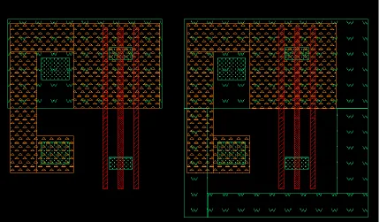
Figure 9: Common well contact for two inverters
Consider the sample layout in Figure 9. The layout consists of two separate inverter
circuits. Notice that a common well is created for two sets of NFinFETs and PFinFETs. (This
is perfectly allowed and this circuit passes LVS check) Figure 10 displays the same circuit
Figure 10: Common well contact for two inverters - only FEOL layers shown
Consider another layout of two inverter circuits but this time having a bulk contact of
Figure 11: Two inverter circuits with separate well contacts (generates LVS errors)
Figure 13: Solution for creating multiple well contacts
As described earlier, an absence of nwell is considered as a pwell. That means in the
whole layout area, there can only be one well contact as there is only one shape, where there
is no nwell. This would cause problems for defining substrate /well contacts on different nets.
Hence, one solution is to create another shape which can be considered as a pwell. This can
be done as shown in Figure 13. Enclosing the pwell contact for one device by nwell creates
two geometries for pwell and hence two well contacts can be created. This concept can be
extended for multiple pwell contacts.
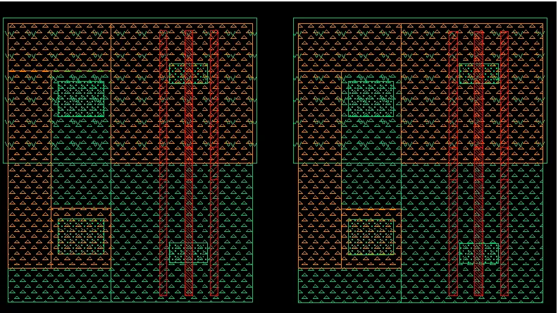
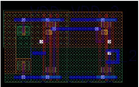
4.2.2. Gate Cut Layer
GATEC is one of the layers in the layer stack that is actually used as a cut mask but
not to remove extra features introduced by SADP uniform patterning. There are separate cut
masks for that. Layer GATEC is used a cut layer specifically for gates. When layouts are
created for multiple gates and stacked together to form a dense layout, gate connectivity is
passed from a top device to the bottom device to save on the area overhead. However, the
same gate connectivity is not desired for all devices. Some other devices might be connected
to opposite clock-phases and hence require a break of connectivity. GATEC is used to chop a
continuous GATEA/GATEB/GATEAB shape into smaller ones with different connectivities.
In the following layout, there are four inverters separately placed and tiled so that
they share the same poly layers – GATEA/GATEB/GATEAB. However, they are driven
separately and hence it is crucial for the connectivity to not pass from one GATE layer to the
other. The GATEC cut mask (green) in the center is used for such situations. This allows to
create denser layouts as many different devices can share the same poly layer and GATEC
Figure 17: Gate Cut Mask (GATEC) example - only FEOL layers shown
The middle-of-line layers are used to decrease the contact resistance and other
parasitics that spring out from the contact to FEOL layers. The MOL layer rules for FreePDK15™ state that AIL1 acts as the first local interconnect to the Fins. Similarly, GIL
However, AIL2 can act as local interconnect layer to both AIL1 and GIL. Thus, GIL can be
directly connected to M1 using via V0 or via the local interconnect AIL2.
Figure 18: MOL layer connections
directly to the poly layer. However, both AIL1 and GIL are connected to AIL2 before the
connectivity passes to V0 and other higher metal layers.
4.3. BEOL Layers
The BEOL layers rules are simply connectivity rules. Due to the requirement of
multiple patterning, the Intermediate Metal layers and the M1 layers are subdivided into three
layers – MINTn, MINTnA, MINTnB (and similarly M1, M1A, M1B), where n=1-5. The
connectivity is such that any metal layer connects to the one directly upwards in the
hierarchy through the corresponding via. That means all 9 combinations are possible.
M1 – MINT1, M1 – MINT1A, M1 – MINT1B
M1A – MINT1, M1A – MINT1A, M1A – MINT1B
M1B – MINT1, M1B – MINT1A, M1B – MINT1B
Of course all of these connections are through via V1. Similarly this can be extended
for all intermediate metal layers until the semi-global metal layers.
There are no explicit examples for these rules as these connections can be made in
different layouts numerous times.
The use of multiple patterning also leads to the issues generated by misalignment.
Misalignment can be a major issue especially for designs in the sub 22nm node.
Misalignment can cause certain lines to be printed closer to each other while some other lines
to be printed away from each other than the expected design [21]. This can cause variance in
various geometry dependent parasitic capacitances between the lines and these variances due
to misalignment may not be captured by the parasitic extraction tools leading to erroneous
due to time constraints, these variations aren’t addressed by the layout and parasitic
extraction runs in this thesis.
4.3.1. Metal Stitching
Until EUV Lithography process becomes available, multiple patterning is imminent
for the development of sub 32nm technology. In multiple patterning, the layout mask is
divided into multiple (two or more) masks which contain only a part of the pattern on the
original mask. However, this division has to be made quite efficiently. This division of the
pattern is called as coloring scheme and it is very important to have a highly effective
coloring scheme. When the two masks are laid over each other the total pattern must be free
of any design rule violations. In case there are any design rule violations, that part of the
layout must be changed or the coloring scheme must be changed. If changing the coloring scheme doesn’t solve the problem and changing that part of the layout adds an area overhead,
metal stitching can be used to resolve the violations. Splitting up a polygon into multiple parts is known as ‘stitching’ and the location where the different masks join is called as a
‘stitch’. Although such stitches decrease the yield to some extent, they can be used to create
densely packed layouts with optimum coloring scheme [22].
Metal stitching is also incorporated into FreePDK15™, with different
colors/sublayers of the same layer (multiple patterning layers) connecting one another. For
Figure 19: Metal Stitching example
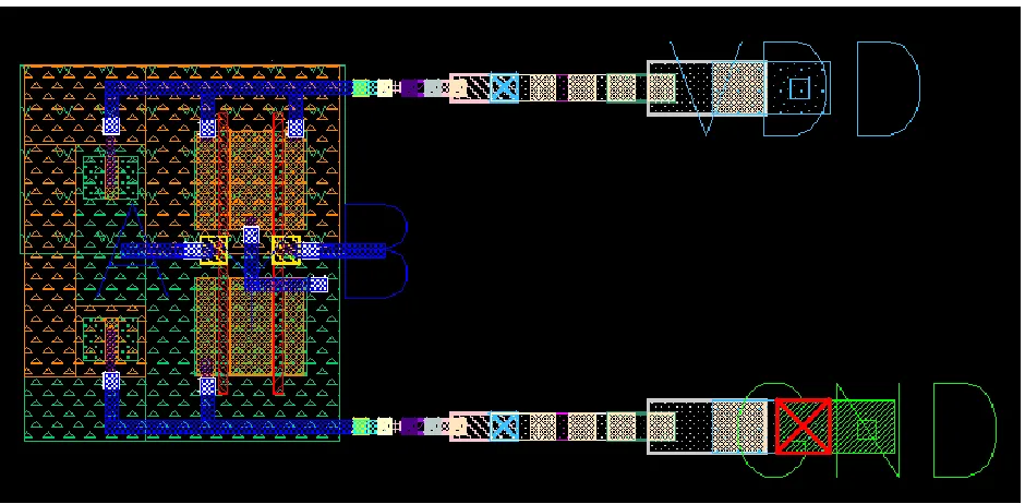
In the layout shown in Figure 19, we have two circuits with one common net and
other individual nets. Layouts are generally created in a highly efficient manner, with high
density and closely packed structures, to save on valuable silicon area. However, the layouts
still follow certain design rules of minimum spacing and extension etc. Consider in the case
of the example, nets VDD and VDD_2, which are individual to each circuit come very close
to each other. Since they are at the same metal hierarchy level, this would generate a
violation of the minimum spacing rule. Multiple patterning may be used to solve this issue
very easily as with multiple patterning each of these nets could be modeled with a different
alone will not be able to solve the problem. Figure 20a) zooms in on the area and removes all
other layers for more clarity.
Figure 20: Metal Stitching example a) Problem b) Solution
All the nets are on M1 layer. VDD and VDD_2 nets are individual to each circuit,
while ZN is the common net for both the circuits. Now, multiple patterning could solve the
problem, if net ZN was not in the picture. However, with net ZN causing additional design
rule violations with both nets VDD and VDD_2, multiple patterning will not do much good
on its own. In such situations, either we could redesign the whole layout and increase the area
or we could utilize a stitch. A stitch is formed, when basically, geometries of two colors of
the same layer overlap. A stitch can cause decrease in yields but can still save on area as
described. Figure 20b) can act as a solution where, ZN is modeled half as an M1layer color A
and the other half as Color B.
A two input NAND layout is created considering all the various rules and is subjected
The SPICE netlist extracted from the LVS run is as below,
* SPICE NETLIST
***************************************
.SUBCKT NAND2 GND VDD A Y B
** N=6 EP=5 IP=0 FDC=4
M0 6 A GND GND nfet L=2e-08 W=2.08e-07 nfin=6 adej=2.4e-15 asej=2.4e-15 pdej=6e-07
psej=6.48e-07 $X=551 $Y=288 $D=0
M1 Y B 6 GND nfet L=2e-08 W=2.08e-07 nfin=6 adej=2.4e-15 asej=2.4e-15 pdej=6.48e-07
psej=6e-07 $X=671 $Y=288 $D=0
M2 Y A VDD VDD pfet L=2e-08 W=2.08e-07 nfin=6 adej=2.4e-15 asej=2.4e-15
pdej=6e-07 psej=6.48e-pdej=6e-07 $X=551 $Y=596 $D=1
M3 VDD B Y VDD pfet L=2e-08 W=2.08e-07 nfin=6 adej=2.4e-15 asej=2.4e-15
pdej=6.48e-07 psej=6e-07 $X=671 $Y=596 $D=1
.ENDS
5. Parasitic Extraction
The semiconductor industry, right from the modest early 70’s till date, has spent millions of dollars and countless efforts in order to stick to the Moore’s Law. Devices have
shrunk down from the size of our palms till deep into the sub-micron range, and it continues
to do so. Although broadly speaking, until the addition of middle-of-line local interconnect
layers, the technology stack has consisted of two sub-stacks, in a way, the device and the
metal interconnects, these sub-stacks have themselves evolved over time and become more
and more complex. Many layers have decomposed to give way to sub-layers, local
interconnects, while multiple-patterning in the sub-micron nodes have added even more
complexity and that has resulted into a highly complex layer stack, like the one we have for
the 15nm node. The shrinking of devices has increased the effect parasitics have, on the chip
performance.
A simple wire segment, or interconnect, connecting two subcircuits or devices, when
fabricated onto a wafer, contributes to the performance of the circuit and adds to delays and
energy losses. A short segment of interconnect possesses a small amount of resistance and
inductance, while along with the dielectric surrounding it, creates a stray capacitance with
any other neighboring interconnects. Moreover, these elements are distributed over the length
of the line and hence a simplistic wire model shown in Figure 22b) doesn’t take into
Figure 22: Interconnects a) Physical view [23] b) Interconnect Model [23]
Smaller chips and denser layouts have increased the length of metal interconnects that
connect various devices together and with that the parasitics associated with these
interconnects have gone up. Device scaling has directly resulted into smaller contacts and
hence larger contact resistances. This, coupled with the large stacks of metal interconnects
has led to a steady rise in the wire line resistance and the compact layer arrangement has
intensified the line-to-line crosstalk [24]. This exponential ascent of parasitics has adversely
affected circuit performance with respect to noise, speed, energy consumption, accuracy and
reliability [23]. As a result, a crucial part of physical verification involves accurate analyses
of interconnects and their parasitics in order to gain a better insight on the chip performance.
Parasitic extraction is therefore, a critical step in the verification flow after a
inductances. A circuit simulation accounting for this convoluted network of parasitics can
lead to a more accurate prediction as to the performance of the circuit.
The flow for parasitic extraction using Mentor Graphics’ Calibre xRC and Calibre
xCalibrate tools is described below.
The technology layer stack is completely described in a technology file (here, a .mipt
file). All the physical and electrical characteristics of the layer stack, like the resistivities for
various conductor layers, permittivities for different dielectrics used, spacing rules from the
design rule deck etc. are put together and simulated to obtain encrypted rule files (here,
rules.C and rules.R). These along with the Layout-versus-Schematic Rule Deck act as a xRC
Rule Deck. The layout and the schematic netlist (which acts as a source) are input to the
Calibre xRC tool and based on the xRC Rule Deck described, the tool populates the netlist
with a parasitics corresponding to all the geometries in the design.
5.1. The .mipt file
As described earlier the technology file, henceforth referred as the .mipt file (as that is
the one used in FreePDK15™), provides all the electrical and physical characteristics of the
layer stack. Geometrical characteristics like minimum-drawn widths, spacing and layer
thicknesses are of crucial importance and are required for a complete simulation. Other
optional geometrical characteristics like, via enclosures, trapezoidal shapes for layers, etc. are
optional but can be specified for a highly accurate simulation. Electrical properties that are
mandatory include resistivities (or sheet resistances), permittivities for various dielectric
layers (dielectric constants), via and contact resistances. All the layers that contribute to the
parasitics must be specified in the .mipt file and the exact same layer names must be used.
The various layers are defined as either conductor, diffusion, dielectric, poly, local
interconnect, vias or contacts based on their properties. Calibre xCalibrate uses these layers
Note: For FreePDK15™, two .mipt files are created, one having the names of all the layers in the technology stack and the other one which has a compact layer list. Multiple patterning
layers for metals are not included in the file with a compact layer list. The reason to do this is
that the rule files generated when the complete stack is simulated by the xCalibrate tool, are
very large and it takes about 28-30 minutes to run a single parasitic extraction run on a circuit
as small as a NAND GATE as compared to about 2 minutes with the compact layer stack.
Hence, the compact layer stack is used. Multiple patterning is very crucial for fabrication but
for parasitic extraction runs, the layout can be modified to only contain the layers in the
compact stack and later on converted back to using the multiple patterning layers after the
5.1.1. FEOL and MOL Stack
Table 2: FEOL and MOL Layer Properties
Layer Name
/Type in .mipt
file Thickness (nm) Resistivity (ohm-m) Relative Dielectric Permittivity Minimum Width (nm) Minimum Spacing (nm)
ACT/diffusion 30
5e-08
(Assumed)
7 96 32
GATE/poly
30
(over
ACT)
7e-08 7 14,16,20 44
AIL1/local
interconnect
50 7e-08 7 28 36
AIL2/local
interconnect
85 7e-08 3.9 24 40
GIL/local
interconnect
105 7e-08
7 (thickness
common to AIL1)
3.9 (thickness
common to AIL2)
56 40
gate-oxide
/dielectric
Table 2 provides all details of the FEOL and MOL layers that are used in the technology stack for FreePDK15™. The oxide layer is not in the technology stack and its
properties are assumed. The width and spacing rules are developed taking into consideration
the predictions in ITRS 2011 roadmap [4] for the 2016 node and the results in [17].
The FEOL and MOL layers - Active, Gate and Local Interconnect Layers are added
first as the general structure of the .mipt file is bottom-to-top. The FEOL and MOL layers
can be seen in Figures 24a) and 24b). The Stack-Viewer which is a part of the Calibre
xCalibrate tool, overlaps layers that are the same z-coordinate and does not allow parallel
stacks. The overlapping does not mean that the layers are shorted together, as the .mipt file
simply dictates the z-coordinates of various layers while the x and y coordinates are obtained
from the layout (.gds or .db file). Figures 24a) and 24b) show two different stacks for the
FEOL and MOL layers, one extracting connectivity from the GATE layers through the
Gate-Interconnect Layer (GIL) while the other extracting connectivity from the fins (ACTIVE)