ISSN (Print) : 2347 - 6710
I
nternationalJ
ournal ofI
nnovativeR
esearch inS
cience,E
ngineering andT
echnology Volume 3, Special Issue 3, March 20142014 International Conference on Innovations in Engineering and Technology (ICIET’14)
On 21st&22ndMarch Organized by
K.L.N. College of Engineering, Madurai, Tamil Nadu, India
Copyright to IJIRSET www.ijirset.com 221
A Positive Buck-Boost DC-DC
Converter with Mode-Select
Circuit Using PID Controller
K.Vijaykaran
1, Mrs.J.Jeyashanthi
2,
M.E .Power Electronics& Drives, Department of EEE, Sethu Institute of Technology, Pulloor, Kariapatti, Virudhunagar, Tamilnadu, India.
M.E .Power Electronics& Drives, Department of EEE, Sethu Institute of Technology, Pulloor, Kariapatti, Virudhunagar, Tamilnadu, India.
ABSTRACT— The proposed work is to design a
positive buck-boost converter with mode-select circuit and with wide range of input voltages. Four switches produce more switching and conduction losses when the converter operates in high frequency. In order to avoid those losses, we employ mode-select circuit in which the converter can work in three different modes as buck, boost and buck-boost mode. With the mode-select circuit the losses in switches are reduced and by the way the converter efficiency is improved. To lessen the loss of switches as the positive buck-boost converter operates in wide range of supply voltages, it is essential to avoid power converters operating in buck-boost mode. By implying feed-forward techniques, the proposed converter can improve its transient response when the supply voltages are changed. It is typically used to compensate for input variations and provide tighter control response of the output voltage. With the above mentioned techniques the proposed converter can get better power efficiency and extends the battery life. The proposed work was simulated by using MATLAB R2012a (v.7.14).
KEYWORDS— Mode-Select Circuit, Feed-Forward Techniques, Positive Buck-Boost Converter.
I. INTRODUCTION
Recently, with the flourishing of portable devices and the development of semiconductor manufacturing technology, conversion efficiency, power consumption and size of devices have become the most important design criteria of switching power converters. Power converters are often applied to LED products, notebooks, mobile phones, and car electronic products. For portable
applications, in order to provide consumers better conveniences, how to extend battery life and improve the conversion efficiency of power converters are challenges for designers. Therefore, it is essential to develop accurate switching power converters, which can reduce more wasted power energy [1]. A very common power handling problem, especially for portable applications, powered by batteries such as cellular phones, personal digital assistants (PDAs), wireless and digital subscriber line (DSL) modems, and digital cameras, is the need to provide a regulated non-inverting output voltage from a variable input battery voltage. The battery voltage, when charged or discharged, can be greater than, equal to, or less than the output voltage. But for such small-scale applications, it is very important to regulate the output voltage of the converter with high precision and performance. Thus, a trade-off among cost, efficiency, and output transients should be considered [6]. A common power handling issue for space-restrained applications powered by batteries is the regulation of the output voltage in the midrange of a variable input battery voltage [11]. There are various topologies such as inverting buck-boost converters, single-ended primary inductance converters (SEPICs), Cuk converters, isolated buck-boost converters and cascaded buck and boost converters, which can be implemented to maintain a constant output voltage from a variable input voltage.
Copyright to IJIRSET www.ijirset.com 222 designing such power supplies. The advantage of having
higher efficiency is longer runtime at a given brightness level from the same set of batteries.
With increasing low-voltage portable devices and growing requirements of functionalities embedded into devices, efficient power management techniques are required to extend battery life. In order to effectively use the remaining capacity of the battery, the design of dc-dc converters need to supply the portable devices a regulated voltage over a wide battery voltage. The limitations of standard analog pulse width modulator (PWM) causes uncontrolled pulse skipping and significantly increased output voltage ripples when the converter operates in the transition region of the buck and boost modes.
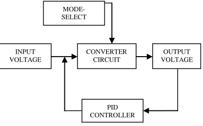
Fig. 1 Block diagram of proposed work.
That is, a buffer region, which is buck-boost mode, is required to provide a smooth and stable transition between two modes. The converter can operate in buck, buck-boost and boost modes when the battery voltage decreases. Since the dc-dc converter has different operation modes, the system stability, the output ripple, and the accuracy of the regulated output voltage during mode transition need to be guaranteed [3].
II. PROPOSED METHOD
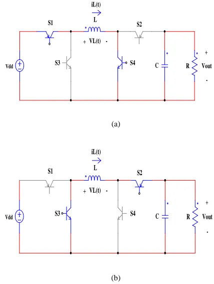
Fig.2 Proposed converter circuit.
In this proposed work, the positive buck-boost converter can operate in buck, boost, and buck-boost mode. The highest ratio occurs in buck-boost mode; the positive buck-boost converter causes switching loss and conduction loss because of its four power transistors. To reduce the loss of switches, as the positive buck-boost
converter operates in wide-range of supply voltages, it is necessary to avoid power converters operating in buck-boost mode. Therefore, we design a mode-select circuit to detect the battery energy and select the operation mode [1]. When the converter operates in buck mode or boost mode, it only switches two power transistors. The mode-select circuit can reduce the conduction loss and switching loss of the proposed converter, and the power efficiency can be improved. The proposed converter can operate in wide supply voltage range and extend the battery life.
A. Mode-Select Circuit
The use of four power transistors produces more switching losses and conduction losses when operated in high frequency. To avoid those losses we utilize mode-select circuit and we can operate in three different modes as buck, boost and buck-boost mode. The mode-select circuit can avoid overlapping of the modes; it can decide the mode to operate when needed. Then it can avoid turning on the power transistors at the same time. Finally, it can determine the operation mode by a control signal from controller. By using this we can extend the battery life and operate the converter in efficient way.
B. Modes of Operation
Fig.3 (a) shows the proposed converter operating in the charging interval of buck mode; the power transistors S1 and S2 are turned ON and the power transistors S3 and S4 are turned OFF. Fig.3 (b) shows the proposed converter operating in the discharging interval of buck mode; the power transistors S2 and S3 are turned ON and the power transistors S1 and S4 are turned OFF. Fig.4 (a) shows the proposed converter operating in the charging interval of boost mode; the power transistors S1 and S4 are turned ON and the power transistors S2 and S3 are turned OFF. Fig.4 (b) shows the proposed converter operating in the discharging interval of boost mode; the power transistors S1 and S2 are turned ON and the power transistors S3 and S4 are turned OFF. Fig.5 (a) shows the proposed converter operating in the charging interval of buck-boost mode; the transistors S1 and S4 are turned ON and the power transistors S2 and S3 are turned OFF. Fig.5 (b) shows the proposed converter operating in discharging interval of buck-boost mode; the power transistors S2 and S3 are turned ON and the power transistors S1 and S4 are turned OFF. (a) Vdd S1 S2 S3 S4 L C R iL(t)
+VL(t)
-Vout +
- S1 S2
Copyright to IJIRSET www.ijirset.com 223 (b)
Fig.3 (a) Charging interval of buck mode. (b) Discharging interval of buck mode.
(a)
(b)
Fig.4 (a) Charging interval of boost mode. (b) Discharging interval of boost mode
(a)
(b)
Fig.5 (a) Charging interval of buck-boost mode. (b) Discharging interval of buck-boost mode.
C. PID Controller
By employing PID controller the converter operates effectively and improves the output voltage, when the supply voltage changes. It gives better performance than PI controller, by reducing rise time and increasing gain value the converter responds faster to changes in set point value.
The PID controller parameter are Kp = 4.5, Ki = 0.01and Kd = 0.001. It reduces the steady state error by compared it with set point voltages for different modes of operation.
TABLE I
CHARACTERISTICS OF PID CONTROLLER
III. SIMULATION RESULTS
A Positive buck-boost dc-dc converter with mode-select circuit using PID controller has been simulated and results were obtained. The output voltage is different for all the three modes as 6v for buck mode, 24v for boost mode and either 6v or 24v for buck-boost mode. Fig.6. shows the simulation circuit of proposed converter operating in buck mode. Fig.7. shows the simulation circuit of proposed converter operating in boost mode. Fig.8. shows the simulation circuit of proposed converter operating in buck-boost mode. Fig.9. shows the simulation results of buck mode; supply voltage = 12v, output voltage = 6v. Fig.10. shows the simulation results of boost mode; supply voltage = 12v, output voltage = 24v. Fig.11. shows the simulation results of buck-boost mode; supply voltage = 12v, output voltage = 6v.
S1 S2 S3 S4 L C R Vdd Vout iL(t) VL(t) + -+ -S1 S2 S3 S4 L C R Vdd Vout iL(t) VL(t) + -+ -S1 S2 S3 S4 L C R Vdd Vout iL(t) VL(t) + -+ -S1 S2 S3 S4 L C R Vdd Vout iL(t) VL(t) + -+ -S1 S2 S3 S4 L C R Vdd Vout iL(t) VL(t) + -+ -Closed
Loop Rise time Overshoot
Settling
time SS-error
Kp Decrease Increase Small
change Decrease
Ki Decrease Increase Increase Decrease
Kd
Small
change Decrease Decrease
Copyright to IJIRSET www.ijirset.com 224 Fig.6 Simulation circuit of proposed converter operating in buck mode.
Fig.7 Simulation circuit of proposed converter operating in boost mode.
Fig.8 Simulation circuit of proposed converter operating in buck-boost mode.
Copyright to IJIRSET www.ijirset.com 225 Fig.10 Simulation results of proposed converter operating in boost
mode.
Fig.11 Simulation results of proposed converter operating in buck-boost mode
IV. CONCLUSION
Thus the implementation of a positive buck-boost converter with mode-select circuit and with wide range of input voltages is proposed in this paper. Four power transistors produce more conduction losses and switching losses when operated in high frequency. To avoid those losses in switches we employ mode-select circuit. By using mode-select circuit we can operate the converter in three different modes as buck, boost and buck-boost mode. By this we can minimize the losses in switches and operate the converter in efficient way. To minimize the loss of switches, as the positive buck-boost converter operates in wide range of input voltages, it is necessary to avoid power converters operating in buck-boost mode. Therefore, we design mode-select circuit to detect battery energy and select the operating mode. Using feed-forward techniques, the proposed converter can improve its transient response when the supply
voltage changes. It is typically used to compensate the input variations and provide tighter control response of the output voltage. By using the above mentioned techniques, the proposed converter improves power efficiency and extends the battery life.
REFERENCES
[1] J. -J. Chen, P. –N. Shen, and Y. –S. Hwang, “A high efficiency positive buck-boost converter with mode-select circuit and feed-forward techniques”, IEEE Trans. Power Electron., vol. 28, no. 9, Sep. 2013.
[2] R. Guo, Z. Liang, and A. Q. Huang, “A family of multimodes charge pump based dc-dc converter with high efficiency over wide input and output range”, IEEE Trans. Power Electron., vol. 27, no. 11. pp. 4788-4798, Nov. 2012.
[3] P. C. Huang, W. Q. Wu, H. H. Ho, and K. H. Chen, “Hybrid buck-boost feed-forward and reduced average inductor current techniques in fast line transient and high efficiency buck-boost converter,” IEEE Trans. Power Electron., vol. 25, no. 3, pp. 719-730, Mar. 2010.
[4] Y. Lee, S. Huang, S. Wang, W. Wu, P. Huang, H. Ho, Y. Lai, and K. Chen, “Power-tracking embedded buck-boost converter with dynamic voltage scaling for the SoC system,” IEEE Trans. Power
Electron., vol. 27, no. 3, pp. 1271-1282, Mar. 2012.
[5] C. F. Lee, and P. K. T. Mok, “On-chip current sensing technique for CMOS monolithic switching-mode power converter,” in Proc.
IEEE Int. symp. Circuits syst., May. 2002, pp. 265-268.
[6] Y. -J. Lee, AlirezaKaligh, ArindamChakraborty, and Ali Emadi, “Digital combination of buck and boost converters to control a positive buck-boost converter and improve the output transients,”
IEEE Trans. Power Electron., vol. 24, no. 5, May, 2009.
[7] P.-J. Liu, J.-N, Tai, H. -S. Chen, and Y.-J. E. Chen, “Spur-reduction design of frequency-hopping dc-dc converters,” IEEE Trans.
Power Electron., vol. 27, no. 11, pp. 4763-4771, Nov. 2012.
[8] S. Maity, and Y. Suraj, “Analysis and modeling of an FFHC- controlled dc-dc buck converter suitabl for wide range of operating conditions,” IEEE Trans. Power. Electron., vol. 27, no. 12, pp. 4914-4924, Dec. 2012.
[9] C.Restrepo, J. Calvente, A. Cid-Pastor, A. E. Aroudi, and R. Giral, “A non-inverting buck-boost dc-dc switching converter with high efficiency and wide bandwidth,” IEEE Trans. Power Electron., vol. 26, no. 9, pp. 2490-2503, Sep. 2011.
[10] C. Restrepo, J. Calvente, A. Romero, E. Videl-Idiarte, and R. Giral, “Current-mode control of a coupled inductor buck-boost dc-dc switching converter,” IEEE Trans. Power Electron., vol. 27, no. 5, pp. 2536-2549, May. 2012.
[11] B. Sahu, and G. A. Rincon-Mora, “A low-voltage, dynamic, non-inverting synchronous buck-boost converter for portable applications,” IEEE Trans. Power Electron., vol. 19, no. 2, pp. 443-452, Mar. 2004.
[12] C. L. Wei, C. -H. Chen, K. C. Wu, and I. T. Ko, “Design of an average-current mode non-inverting buck-boost dc-dc converter with reduced switching and conduction losses,” IEEE Trans.
Power Electron., vol. 27, no. 12, pp. 4934-4943, Dec. 2012.
[13] C. Yao, X. Ruan, X. Wang, and C. K. Tse, “Isolated buck-boost dc-dc converters suitable for wide input-voltage range,” IEEE
Trans. Power Electron., vol. 26, no. 9, pp. 2599-2613, Sep. 2011.
[14] V. Yousefzadeh, A. Babazadeh, B. Ramachandran, E. Alarcon, L. Pao, and D. Maksimovic, “Proximate time-optimal digital control for synchronous buck dc-dc converters,” IEEE Trans. Power. Electron., vol. 23, no. 4, pp. 2018-2026, Jul. 2008.
[15] K. K. I. Hwu, and T. T. J. Peng, “A novel buck-boost converter combining KY and buck converters,” IEEE Trans. Power
Electron., vol. 27, no. 5, pp. 2236-2241, May. 2012.
Copyright to IJIRSET www.ijirset.com 226 PID and fuzzy controllers for dc-dc converters,” IEEE Trans.
Ind. Electron., vol. 56, no. 6, pp. 2237-2248, Jun. 2009.