ISSN (Online) : 2319 - 8753 ISSN (Print) : 2347 - 6710
International Journal of Innovative Research in Science, Engineering and Technology
Volume 3, Special Issue 3, March 20142014 International Conference on Innovations in Engineering and Technology (ICIET’14)
On 21st & 22nd March Organized by
K.L.N. College of Engineering, Madurai, Tamil Nadu, India
Performance Evaluation Of OCC’ed Single-Phase
Inverter For Grid Connected PV System
Jaysing A. Kshirsagar
1, K.Vadirajacharya
21M.Tech Student, Department of Electrical Engineering, Dr. Babasaheb Ambedkar Technological University,
Lonere, Maharashtra,(India).
2Associate Professor, Department of Electrical Engineering, Dr. Babasaheb Ambedkar Technological University,
Lonere, Maharashtra, (India).
ABSTRACT— Recent years, electricity sector is
reforming along with various renewable energy promotion policies has increased the importance of small grid-connected photovoltaic (PV) systems utilizing stage phase inverters. This paper propose a single-stage inverter with maximum power point tracking (MPPT) and one cycle control (OCC) for grid connected (PV) system. This control scheme is based on the output current-adjusting feature of one cycle control. The output current of inverter can be adjusted according to the voltage of the photovoltaic (PV) array so as to extract the maximum power from it. Schemes based on one cycle control (OCC) which do not require the service of a phase locked loop for interfacing the inverter to the grid are increasingly being employed for such applications. However, the OCC-based schemes reported earlier require sensing of the grid voltage which somewhat offsets one of the inherent strengths of OCC-based systems. In an effort to overcome the above limitation, an OCC based grid connected single-stage PV system is proposed in this paper which does not require sensing the grid voltage. Further, it requires less no. of sensors (two) as compared to that required (four) in the earlier reported scheme for the implementation of the core controller comprising of OCC and MPPT blocks. The viability of the proposed scheme is confirm by performing simulation and results validation.
KEY WORDS— One Cycle Control (OCC); Maximum
Power Point Tracking (MPPT); PV array; Single phase grid connected inverter.
I.
I
NTRODUCTIONSolar photovoltaic (PV) based systems are increasingly being used for electricity production in the context of global warming, climate change, and rapid exhaustion of fossil fuels. A portion of the huge gap between the expected demand and availability of the electricity to be
met from renewable energy sources like solar PV. Further, the renewable energy promotion policies across different parts of the globe, like feed-in tariff, renewable portfolio, standard, net metering, etc. Photovoltaic (PV) systems are ideal distributed generation (DG) units, and they offer many advantages such as no fuel costs, no pollution, no noise, and little maintenance. [1], are providing considerable incentives even to individual single phase customers to install solar PV panels and sell the excess power generated to the utility. A reliable and low cost single phase grid connected inverter which require little maintenance has become the order of the day for interfacing such low capacity systems to grid.
Copyright to IJIRSET www.ijirset.com 62 voltages [5]. In an effort to simplify the control structure
of grid-connected inverters in a PV system, schemes based on OCC have been proposed [3], [4]. Systems based on OCC do not require the service of a PLL [6]. The one cycle controlled single phase inverter is very suitable for realisation and controlling the maximum power from the solar array is very sensitive to the set of design parameters. One cycle controller requires less number of sensors (two) as compared to that required (four) in [4] for the implementation of the core controller comprising of OCC and MPPT blocks.
II.
P
ROPOSEDVOLATGESENSERLESSOCCBASED INVERTERFORPVSYSTEM
A single-stage grid connected PV system [7] having a single-phase full bridge voltage source inverter is shown in Fig. 1. The inverter switches are controlled to generate output voltage from the inverter whose fundamental component is VI.
S1
S2
S4
S3
L
Vs
PV Array +
_
Is
Vi
Vdc
Fig. 1 Single-stage single-phase grid-connected PV system.
CONVERTER
jLw
Vs 0 Vdc
Is
Vi1 δ
P
Fig. 2 Phaser model of Grid connected system
By controlling the magnitude and phase of VI through a
proper pulse width modulation strategy, the power flow from the solar array to the grid can be controlled while maintaining a high power factor and low harmonic distortion. Considering the phasor model of the system shown in Fig. 2 and assuming the system to be lossless, the expression for real power flow from the inverter to the grid can be expressed as follows:
(1)
where Vs is the rms grid voltage, ω is the grid frequency,
and δ is the phase angle between the fundamental component of the output voltage of the inverter and the
grid voltage. The inverter, however, cannot be controlled with the basic OCC-based control technique as basic OCC based schemes exhibit instability in operation when the converter involved is operated in an inverting mode of operation [8]. In order to overcome this problem, a modified OCC ( M-OCC ) -based on scheme has been reported in [8]. Although the scheme presented in [8] does not require the service of a PLL, it needs to sense instantaneous grid voltage similar to the case of [4]. In the scheme reported in [8], the sensed grid voltage is multiplied by a constant gain to generate a fictitious current signal if in phase with the grid voltage. This fictitious current signal is then added to the actual current drawn by the inverter. The sum of these two signals is then used by the OCC core controller to generate gating pulses for the inverter switches.
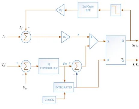
2nd-Order BPF Rp-1
Rs
PI CONTROLLER
INTEGRATER
R
S Q
Q
CLOCK
S1 S3
S2 S4
+
_
+ +
_ X
Vm _
_
I s
Vdc*
Vdc
I f
Fig. 3 Control block diagram of the proposed scheme
The scheme proposed in this paper does not sense the grid voltage to generate the fictitious current signal required to circumvent the issue of instability in OCC based inverter. It synthesizes the fictitious current signal required by multiplying the fundamental component of the inverter output voltage with a constant gain. Information regarding the inverter output voltage is obtained from the switching function used to trigger the inverter switches and not by sensing the inverter output voltage per sec. The schematic control block diagram of the proposed scheme is shown in Fig. 3. The dc-link capacitor voltage is sensed and compared with a set reference, and the error so generated is fed to a proportional and integral regulator to produce a signal Vm. A sawtooth waveform of constant frequency having
a peak to peak value of 2Vm is generated using a
resettable integrator. A free running clock having a time period Ts is used to reset the integrator.The time constant
of the integrator Ti is chosen to be half of Ts. A fictitious
current signal proportional to fundamental component of the output voltage of the inverter (if =VI1/Rp) is added
Copyright to IJIRSET www.ijirset.com 63 In order to obtain VI1 and hence if inverter switching
pulses are passed through a saturator. The output of the saturator pulsates between the scaled dc-link voltage (Vdc)
and zero in tandem with the pulsation of the switching sequence between the states one and zero. The signal proportional to VI is obtained by filtering the output of the
saturator. The harmonic spectrum of saturator output has: 1) A fundamental frequency component (50 Hz); 2) A dc component; and 3) Higher frequency components centered around multiples of switching frequency. Hence, a band pass filter (BPF) is required to retrieve the fundamental component of this signal and filter out the dc and higher order components. A second-order BPF having a central frequency equal to the power frequency (50 Hz) is used for the purpose. The modulating signal is multiplied by a gain Rs and is then compared with the
sawtooth waveform to generate the switching pulses. At every rising edge of the clock pulse, S2 and S4 are turned
on which leads to the increment in source current is. When
the modulating signal becomes equal to the sawtooth waveform, S2 and S4 are turned off and S1 and S3 are
turned on so that the modulating signal and hence is decrease. The rising and falling slopes of is given by (vs+
Vdc)/ L and (vs−Vdc )/L, respectively, where vs is utility
voltage, Vdc is the dc-link capacitor voltage, and L is the
magnitude of the boost inductor.
The modulating signal x is being compared with the saw- tooth waveform to generate the switching pulses. When x is less than the sawtooth waveform, S2 and S4 are
on, and the output voltage of the inverter is −Vdc. When x
is greater than the sawtooth waveform, S1 and S3 are
turned on, and the output voltage of the inverter is +Vdc.
Hence, the average output voltage of the inverter during a switching time period (time period of the sawtooth waveform) is
Therefore, it can be inferred from (3) that the average inverter output voltage in a switching time period is proportional to the modulating signal x. Further, the fundamental component of the output voltage of the inverter will be in phase with the modulating signal. By combining (2) and (3), the expression for inverter output voltage averaged over a switching time period is obtained as follow;
From the aforementioned expression, it can be inferred that VI and isare having a phase shift of either 0◦ or 180◦
between each other.
III.
M
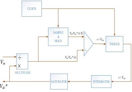
PPTREALISATIONUSINGP&OMETHODP&O method is one of the popular methods to track the maximum power point [9]. Implementation of MPPT by P&O method is generally done by using DSP or microcomputer, but discrete analog and digital circuitry can also be used for the purpose [10]. The analog controller proposed in this paper for the implementation of the P&O algorithm is shown in Fig. 4.
The controller consists of an analog multiplier, a sample- and-hold circuit, a free-running clock, a toggle switch, and an integrator. The P&O controller receives the signal Vm from the OCC controller of Fig. 3. The
output of the P&O controller is Vdc∗ which sets dc-link
voltage reference required by the OCC controller of Fig. 3. An integrator connected to the output of a toggle flip-flop generates the voltage reference Vdc∗. The period of
the P&O cycle is decided by a free-running clock which sets sampling instants for the sample-and-hold circuit and toggling instants for the toggle flip-flop. Depending on the output level of the toggle flip-flop, Vdc∗ can have
either a rising or a falling slope. The rate of change in
Vdc∗ is kept much smaller than the control bandwidth of
the OCC controller. An analog multiplier of low bandwidth is used to perform the division Vm/Vdc. The
signal Vm/Vdc is sampled at the beginning of a period of a
P & O cycle using the sample-and-hold circuit.
Vm
Vdc*
CLOCK
SAMPLE & HOLD
SATURATOR INTEGRATOR
TOGGLE
÷
×
+
_
Vm/Vdc* (t)
Vm/Vdc* (t-T)
+/- Vsat
+/- Vsat
MULTIPLIER
Fig. 4. Control block diagram of MPPT Realization
A comparator compares the current value of Vm/Vdc
with that of its previous value stored in the sample-and-hold circuit. A positive comparator output implies that in the current cycle, the power delivered by the inverter has decreased as per [11] while a negative comparator output indicates an increment in power in the current P&O cycle. Therefore, when the output of the comparator is positive, the slope of Vdc∗ is reversed to that followed in
the previous P&O cycle. Furthermore, if the comparator output is negative, the slope of Vdc∗ is maintained the
same as that of the previous cycle.
IV.
S
IMULATIONANDRESULTSCopyright to IJIRSET www.ijirset.com 64
MATLAB–Simulink platform. In order to objectively show that the proposed voltage sensorless scheme does not have the problem of current instability while operating in the inverting mode of operation, a model of the system shown in Fig. 1 is simulated [7]. The parameters the inverter chosen for the purpose of simulation [7] and the controller are as follows:
Switching frequency: 20 kHz; DC-link capacitor: 2200 µF; Series inductor: 2 mH;
Rp: 1.5Ω; Rs: 0.16Ω;
Quality factor of BPF (Q):2; Control frequency of BPF: 49.8 Hz.
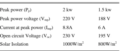
The specifications for the solar array used in the simulation study are provided in Table I, corresponding to 1000W/m2 and 800W/m2 insolation levels. Simulated Performance of PV array during 1000W/m2 insolation level shown in Fig. 5. The dc-link reference is externally set at 220 V. The grid considered as a 230 Vrms 50-Hz system.
Table I
PV ARRAY SPECIFICATIONS
Peak power (Pp) 2 kw 1.5 kw
Peak power voltage (Vmp) 220 V 188 V
Current at peak power (Imp) 8.8A 6 A
Open circuit Voltage (Voc) 230 V 195 V
Solar Isolation 1000W/m2 800W/m2
Fig. 5 Simulated Performance of PV Array during 1000W/m2
insolation level: Voltage, Current and Power
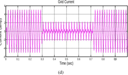
When isolation level abruptly changed from 1000W/m2 to 800W/m2. The DC link voltage is suddenly fall at 188V and current is changed from 8.8A to 6A. And maximum power output of PV array is changed from 2kw to 1.5kw at 3 sec is shown in Table II. After 8 sec, the voltage, current, power is settle back to the initial value. When isolation level abruptly changed from 1000W/m2 to
800W/m2. The DC link voltage is suddenly fall at 188V and current is changed from 8.8A to 6A. And maximum power output of PV array is changed from 2kw to 1.5kw at 3 sec is shown in Table I. After 8 sec, the voltage, current, power is settle back to the initial value. Fig. 6 Shows the Simulation results such as waveforms of the DC link voltage, Grid current, and Grid voltage.
From the simulated performance, it can be inferred that the system supplies the available maximum power from the PV array to the grid. The transient performance of the system can be seen during the change in insolation levels. Moreover, it can be observed from the simulated performance that the changes in PV current and dc-link voltage are smooth during the change in insolation level which implies a satisfactory transient performance for the system.
0 0.1 0.2 0.3 0.4 0.5 0.6 0.7 0.8 0.9 1
0 50 100 150 200 250
Time (sec)
Vo
lt
ag
e
(v
olt
s
)
DC Link Voltage
(a)
0 0.1 0.2 0.3 0.4 0.5 0.6 0.7 0.8 0.9 1
-300 -200 -100 0 100 200 300
Output Voltage of inverter
Time (sec)
Vo
lt
ag
e
(v
olt
s
)
(b)
(c)
0 0.1 0.2 0.3 0.4 0.5 0.6 0.7 0.8 0.9 1
-300 -200 -100 0 100 200 300
Grid Voltage
Time (sec)
Vo
lt
ag
e
(v
olt
s
Copyright to IJIRSET www.ijirset.com 65
0 0.1 0.2 0.3 0.4 0.5 0.6 0.7 0.8 0.91
-6 -4 -2 0 2 4 6
Time (sec)
C
urre
nt
(am
p)
Grid Current
(d)
Fig. 6 Simulated Performance of the system during step changes in
insolation level (1000W/m2 to 800W/m2): (a) DC link Voltage, (b)
Output voltage of inverter, (c) Grid voltage, (d) Output Current.
The steady-state grid voltage, source current, dc-link voltage,and the fictitious current signal obtained from the filtered output of the switching pulses of the inverter are shown in Fig. 6. It can be noted that the grid voltage and source current are almost 1800 out of phase thereby demonstrating the inverting mode of operation. The measured harmonic spectrum of the current supplied by the system to the grid and the grid voltage from which it can be inferred that all the low order harmonics to that of the fundamental component. As an OCC-based scheme poses itself as equivalent impedance to the grid, distortions present in the grid voltage also appear in the current drawn by the system from the grid.
V. CONCLUSION
An M-OCC based Single phase Single-stage voltage senseless grid connected PV system has been proposed. The limitation of the existing OCC based inverters, such as requirement for sensing the grid voltage to tackle the instability problem, is circumvented in the proposed scheme. The proposed scheme is based on a single stage of power con version and is realized by utilizing a considerably less number of sensors compared to that of conventional schemes. Further, the core controller of the proposed scheme can be realized by means of a very simple analog controller. All the aforementioned features of the scheme make it an ideal candidate for small and distributed single-phase grid connected PV systems.
Detailed simulation studies have been carried out to verify the effectiveness of the scheme. The viability of the scheme has been confirmed by performing detailed simulation studies.
REFERENCES
[1] K. H. Solangi, M. R. Islam, R. Saidur, N. A. Rahim, and H. Fayaz,
―A review on global solar energy policy,‖ Renewable Sustainable
Energy Rev., vol. 15, no. 4, pp. 2149–2163, May 2011.
[2] M. Calais, J. Myrzik, T. Spooner, and V. Agelidis, ―Inverters for
single phase grid connected photovoltaic systems—An overview,‖ in Proc. IEEE Power Elec. Spec. Conf., Jun. 2002, pp. 1995– 2000.
[3] M. Fortunato, A. Giustiniani, G. Petrone, G. Spagnuolo, and M.
Vitelli, ―Maximum power point tracking in a one cycle controlled
single stage photovoltaic inverter,‖ IEEE Trans. Ind. Electron.
vol. 55, no. 7, pp. 2684–2693, Jul. 2008.
[4] F. Chen and K. M. Smedley, ―A cost-effective single-stage
inverter with maximum power point tracking,‖ IEEE Trans.
Power Electron., vol. 19, no. 5, pp. 1289–1294, Sep. 2004.
[5] Dezso Sera,, Laszlo Mathe,, Tamas Kerekes, Sergiu Viorel
Spataru, and Remus Teodorescu, ―On the Perturb-and-Observe and Incremental Conductance MPPT Methods for PV Systems‖ IEEE JOURNAL OF PHOTOVOLTAICS, VOL. 3, NO. 3, JULY 2013.
[6] K. Chatterjee, D. V. Ghodke, A. Chandra, and K. Al-Haddad,
―Simple controller for STATCOM-based var generators,‖ IET
Power Electron., vol. 2, no. 2, pp. 192–202, Mar. 2009.
[7] Sreeraj E. S., Kishore Chatterjee, and Santanu Bandyopadhyay,
―One-Cycle-Controlled Single-Stage Single-Phase
Voltage-Sensorless Grid-Connected PV System,‖ IEEE transactions on
industrial electronics, VOL. 60, NO. 3, MARCH 2013.
[8] D. V. Ghodke, K. Chatterjee, and B. G. Fernandes, ―Modified one
cycle controlled bi-directional high power factor AC to DC
converter,‖ IEEE Trans. Ind. Electron., vol. 55, no. 6, pp. 2459–
2472, Jun. 2008.
[9] B. K. Bose, P. M. Szezesny, and R. L. Steigerwald,
―Microcontroller control of residential photovoltaic power
conditioning system,‖ IEEE Trans. Ind. Appl., vol. 21, no. 5, pp.
1182–1191, Sep. 1985.
[10] G. Petrone, G. Spagnuolo, R. Teodorescu, M. Veerachary, and M.
Vitelli, ―Reliability issues in photovoltaic power processing
systems,‖ IEEE Trans. Ind. Electron., vol. 55, no. 7, pp. 2569–
2580, Jul. 2008.
[11] N. Femia, M. Fortunato, G. Petrone, G. Spagnuolo, and M. Vitelli,
―Dynamic model of a grid-connected photovoltaic inverter with
one cycle control,‖ in Proc. 35th Annu. Conf. IEEE Ind. Electron.,
Nov. 2009, pp. 4561–4565.
[12] Vadirajachrya. K, Agarwal Pramod and Gupta H. O. ―Unified