A High Performance System on Chip Bus
Design and Verification
K.P.Anish, M.Maria Rubiston
PG Student, Department of ECE, Rajas Engineering College, Raja Nagar, Vadakkangulam, Tamil Nadu, India
Assistant Professor, Department of ECE, St. Joseph College of Engineering, Chennai, Tamil Nadu, India
ABSTRACT: A High-Performance system-on-chip bus protocol termed the master-slave bus (MSBUS).Reduce the inevitable trade off among area, throughput and energy efficiency. The control bus is developed as a cost and low-power bus, and the data bus is created as a high-throughput full-duplex bus with the feature of block data transfer. To evaluate the bus performance, we create four analytical models including transfer time consumption (TC), wire efficiency (WE), valid data bandwidth (VDB) and dynamic energy efficiency.
I. INTRODUCTION
1.1 Efficient Exploration of Bus-Based System-on-Chip Architectures:
Separation between computation and communication in system design allows system designers to explore the communication mapping decision is made. In this paper, we present an iterative two-step exploration methodology for bus-based on-chip communication architecture independently after component selection and for multitask applications. We assume that the memory traces from the processing components are given. The proposed methodology uses a static performance estimation technique extended for multi task applications to reduce the design space quickly and drastically and applies a trace-driven simulation to the reduced set of design candidates for accurate performance estimation. For the case that local memory traffics as well as shared memory traffics are involved in bus contention, memory allocation is considered as an important axis of the design space in our technique. Experimental results show that the proposed methodology achieves significant performance gain by optimizing on-chip communication only, up to almost 100% compared with an initial single shared bus architecture, in both two real-life examples, a four-Channel digital video recorder and an equalizer for OFDM DVB-T receiver.
1.2 Dynamically Configurable Bus Topologies for high performance on-chip Communication:
A major challenge in the design of multi core embedded systems is how to tackle the communications among tasks with performance requirements and precedence constraints. In this paper, we consider the problem of scheduling real-time tasks. We show that the problem is NP-hard and determine the best possible approximation ratio of approximation algorithms. First, we propose a polynomial-time optimal algorithm for a restricted case where one multilayer bus. The result is then extended as a pseudo polynomial-time optimal algorithm to consider multiple multilayer buses with arbitrary execution and communication times, as well as different timing constraints and objective functions. We compare the performance of the proposed algorithm with that of some popular heuristics, and provide further insights into the multilayer bus system design.
1.3 Implementation of a Self-Motivated Arbitration Scheme for the Multilayer AHB Bus matrix:
the nine possible arbitration schemes based upon the priority-level notifications and the desired transfer length from the masters so that arbitration leads to the maximum performance. Experimental results show that, although the area overhead of the proposed SM arbitration scheme is 9%-25% larger than those of the other arbitration schemes, our arbiter improves the throughput by 14%-62% compared to other schemes.
1.4 Wire Optimization for Multimedia SoC and SiP Design
With advances in VLSI integration technology, a large number of hardware components can be integrated into a single chip. To provide the communication bandwidth for these components, existing bus-based interconnects often suffer from a large area occupied by a large number of bus signals. To address this issue, this paper proposes a new protocol for on-chip or in-package communication that is termed the system-on-chip network protocol (SNP). SNP uses a small number of signals that are shared by address, control, and data information. Additional three-bit phase signals are used to distinguish the different information transmitted through a single set of SNP signals. Two sets of identical SNP signals form a symmetric communication channel that allow a master-to-master type of communication between hardware components. The phase signals facilitate the reduction of the communication time with phase interleaving and phase omission-restoration among successive transactions. The efficiency of SNP is evaluated by a static performance analysis as well as by simulations with register-transfer level models of SNP components. Both the analysis and simulation results show that the communication time with SNP is approximately a half that of advanced microcontroller bus architecture advanced high-performance bus (AHB), although SNP has wires that are approximately three-fifths of AHB. MPEG-4 chips are implemented with both AHB and SNP, respectively, and it is observed from the MPEG-4 implementations that SNP requires less area for communication compared to AHB.
1.5 High-level power modelling, estimation, and optimization
Silicon area, performance, and testability have been, so far, the major design constraints to be met during the development of digital very-large-scale-integration (VLSI) systems. In recent years, however, things have changed; increasingly, power has been given weight comparable to the other design parameters. This is primarily due to the remarkable success of personal computing devices and wireless communication systems, which demand high-speed computations with low power consumption. In addition, there exists a strong pressure for manufacturers of high-end products to keep power under control, due to the increased costs of packaging and cooling this type of device. Last, the need of ensuring high circuit reliability has turned out to be more stringent. The availability of tools for the automatic design of low-power VLSI systems has thus become necessary. More specifically, following a natural trend, the interests of the researchers have lately shifted to the investigation of power modelling, estimation, synthesis, and optimization techniques that account for power dissipation during the early stages of the design flow. This paper surveys representative contributions to this area that have appeared in the recent literature.
1.6 Wireless LAN Medium Access Control (MAC) and Physical Layer (PHY) specifications
This amendment defines security mechanisms for IEEE 802.11. It includes a definition of WEP for backward compatibility with the original standard, IEEE Std 802.11, 1999 Edition. It defines TKIP and CCMP, which provide more robust data protection mechanisms than WEP affords. This amendment introduces the concept of a security association into IEEE 802.11, and defines security association management protocols called the 4-Way Handshake and the Group Key Handshake. Finally, it specifies how IEEE 802.1X may be utilized by IEEE 802.11 LANs to effect authentication.
1.7 Power aware interface synthesis for bus-based SoC designs:
heuristic is able to reduce power consumption on the wires by about 28% on the average from an initial design having single layer bus architecture.
II. PROPOSED SYSTEM
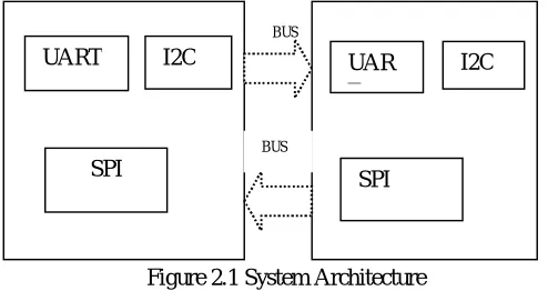
MSBUS-based Direct Memory Access (DMA) is designed at the RTL. As the only slave of SBUS, the SBUS DMA supports both the linear and block transfers, and provides the command pre-processing scheme. There are two separate queues of the SBUS DMA, one write queue and one read queue, and the depth is four of each. Thus, up to eight SBUS commands can be pre-processed and pushed into the command queues after winning the arbitration. In proposed method master slave bus protocol is used. Multiple slave acts as full duplex during data transmission. To verify all the bus-based DMA design which can be both RTL and gate-level net list, a Universal Verification Methodology (UVM)
environment is set up. As an example of MSBUS based SoC several encapsulated, ready-to-use and Configurable
Verification agents are integrated into the test bench. All the six peripherals including NON Flash, UART, I2C, SPI,
GPIO, and timer controllers are MBUSs slaves. They are configured by the microprocessor through MBUS directly. 2.1 BLOCK DIAGRAM
Figure 2.1 System Architecture
In computer architecture, a bus (related to the Latin "omnibus", meaning "for all") is a communication system that transfers data between components inside a computer, or between computers. This expression covers all related hardware components (wire, optical fibre, etc.) and software, including communication protocols. Early computer buses were parallel electrical wires with multiple connections, but the term is now used for any physical arrangement that provides the same logical functionality as a parallel electrical bus. Modern computer buses can use both parallel and bit serial connections, and can be wired in either a multi drop (electrical parallel) or daisy chain topology, or connected by switched hubs, as in the case of USB.
Computer systems generally consist of three main parts: the central processing unit (CPU) that processes data, memory that holds the programs and data to be processed, and I/O (input/output) devices as peripherals that communicate with the outside world. An early computer might use a hand-wired CPU of vacuum tubes, a magnetic drum for main memory, and a punch tape and printer for reading and writing data. In a modern system we might find a multi-core CPU, DDR3 SDRAM for memory, a hard drive for secondary storage, a graphics card and LCD display as a display system, a mouse and keyboard for interaction, and a Wi-Fi connection for networking. In both examples, computer buses of one form or another move data between all of these devices.
It is possible to allow peripherals to communicate with memory in the same fashion, attaching adaptors in the form of expansion cards directly to the system bus. This is commonly accomplished through some sort of standardized electrical connector, several of these forming the expansion bus or local bus. However, as the performance difference between the CPU and peripherals varies widely, some solution is generally needed to ensure that peripherals do not slow overall system performance. Many CPUs feature a second set of pins similar to those for communicating with memory, but able to operate at very different speeds and using different protocols. Others use smart controllers to place the data directly in memory, a concept known as direct memory access. Most modern systems combine both solutions,
BUS
I2C UAR
T I2C
UART
SPI SPI
where appropriate. As the number of potential peripherals grew; using an expansion card for every peripheral became increasingly untenable. This has led to the introduction of bus systems designed specifically to support multiple peripherals.
2.2 UART
A universal asynchronous receiver/transmitter, abbreviated UART is a computer hardware device translates data between parallel and serial forms. UARTs are commonly used in conjunction with communication.A UART is usually an individual (or part of an) integrated circuit (IC) used for serial communications over a computer or peripheral device serial port. UARTs are now commonly included in microcontrollers. A dual UART, or DUART, combines two UARTs into a single chip. An octal UART or OCTART combines eight UARTs into one package, an example being the NXP SCC2698. Many modern ICs now come with a UART that can also communicate synchronously; these devices are called USARTs.The universal asynchronous receiver/transmitter (UART) takes bytes of data and transmits the individual bits in a sequential fashion. At the destination, a second UART re-assembles the bits into complete bytes. Each UART contains a shift register, which is the fundamental method of conversion between serial and parallel forms. Serial transmission of digital information (bits) through a single wire or other medium is less costly than parallel transmission through multiple wires. The UART usually does not directly generate or receive the external signals used between different items of equipment. Separate interface devices are used to convert the logic level signals of the UART to and from the external signalling levels. External signals may be of many different forms. Examples of standards for voltage signalling are RS-232, RS-422 and RS-485 from the EIA. Historically, current (in current loops) was used in telegraph circuits. Some signalling schemes do not use electrical wires. Examples of such are optical fibre, IrDA (infrared), Bluetooth in its Serial Port Profile (SPP). Some signalling schemes use modulation of a carrier signal (with or without wires). Examples are modulation of audio signals with phone line modems, RF modulation with data radios, and the DC-LIN for power line communication.
2.3 SPI
Figure 2.2 SPI bus
SPI devices communicate in full duplex mode using Master-Slave architecture with a single master. The master device originates the frame for reading and writing. Multiple slave devices are supported through selection with individual slave select (SS) lines. Sometimes SPI is called a four-wire serial bus, contrasting with three-two-, and one-wire serial buses. The SPI may be accurately described as a synchronous serial interface, but it is different from the Synchronous Serial Interface (SSI) protocol, which is also a four-wire synchronous serial communication protocol, but employs differential signalling and provides only a single simplex communication channel.The SPI bus can operate with a single master device and with one or more slave devices. If a single slave device is used, the SS pin may be fixed to logic low if the slave permits it. Some slaves require a falling edge of the chip select signal to initiate an action; an example is the Maxim MAX1242 ADC, which starts conversion on a high-low transition. With multiple slave devices, an independent SS signal is required from the master for each slave device.
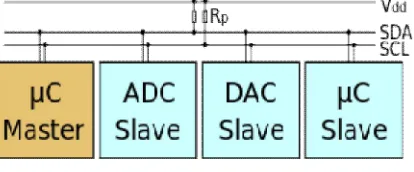
2.4 I2C
I²C (Inter-Integrated Circuit), is a multi-master, multi-slave, single-ended, invented (now NXPSemiconductors). It is typically used for attaching lower-speed peripheral ICs to processors and microcontrollers.
Figure 2.3 I²C Protocol
I²C uses only two bidirectional open-drain lines, Serial Data Line (SDA) and Serial Clock Line (SCL), pulled up with resistors. Typical voltages used are +5 V or +3.3 V although systems with other voltages are permitted.The I²C reference design has a 7-bit or a 10-bit (depending on the device used) address space. Common I²C bus speeds are the 100 kbit/s standard mode and the 10 kbit/s low-speed mode, but arbitrarily low clock frequencies are also allowed. Recent revisions of I²C can host more nodes and run at faster speeds (400 kbit/s Fast mode, 1 Mbit/sFast mode plus or Fm+, and 3.4 Mbit/s High Speed mode). These speeds are more widely used on embedded systems than on PCs. There are also other features, such as 16-bit addressing.
Note the bit rates are quoted for the transactions between master and slave without clock stretching or other hardware overhead. Protocol overheads include a slave address and perhaps a register address within the slave device as well as per-byte ACK/NACK bits. Thus the actual transfer rate of user data is lower than those peak bit rates alone would imply. For example, if each interaction with a slave inefficiently allows only 1 byte of data to be transferred, the data rate will be less than half the peak bit rate.
The maximum number of nodes is limited by the address space, and also by the total bus capacitance of 400 pF, which restricts practical communication distances to a few meters. The before mentioned reference design is a bus with a clock (SCL) and data (SDA) lines with 7-bit addressing. The bus has two roles for nodes: master and slave:
Master node — node that generates the clock and initiates communication with slaves.
Slave node — node that receives the clock and responds when addressed by the master.
III. CONCLUSION
We propose a high-performance bus with reduced interface complexity, minimal power consumption, and high bandwidth. Moreover, we evaluate its performance with four estimation models such as TC, WE, VDB, and DEE during the hardware implementation flow automatically and accurately. Comparing AHB, AXI and MSBUS DMA
implementation as a case study, both the static analysis and the real hardware results demonstrate that MSBUS achieves higher performance, especially in the block transfer mode: the WE of MSBUS is 2.3 times of AXI and 2.4 times of AHB, and the DEE is close to the double of AXI or AHB. The single-processor and multi client bus structure of MSBUS reduces resource utilization and energy consumption and limits the complexity of circuits. Therefore, the MSBUS protocol is very desirable for small-scale embedded systems with requirements of a low-cost interface and high-energy efficiency.
REFERENCES
[1] K. Sekar, K. Lahiri, A. Raghunathan, and S. Dey, “Dynamically configurable bus topologies for high-performance on-chip communication,” IEEE Trans. Very Large Scale Integr. (VLSI) Syst., vol. 16, no. 10, pp. 1413–1426, Oct. 2008.
[2] S. Kim and S. Ha, “Efficient exploration of bus-based system-on-chip architectures,” IEEE Trans. Very Large Scale Integr. (VLSI) Syst., vol. 14, no. 7, pp. 681–692, Jul. 2006.
[3] P.-C. Hsiu, C.-K.Hsieh, D.-N.Lee, and T.-W. Kuo, “Multilayer bus optimization for real-time embedded systems,” IEEE Trans. Comput., vol. 61, no. 11, pp. 1638–1650, Nov. 2012.
[4] J. Lee, “Design methodology for on-chip bus architectures using system on-chip network protocol,” IET Circuits, Devices Syst., vol. 6, no. 2, pp. 85–94, Mar. 2012.
[6] Y.-S. Cho, E.-J.Choi, and K.-R. Cho, “Modeling and analysis of the system bus latency on the SoC platform,” in Proc. Int. Workshop System-Level Interconnect Predict., New York, NY, USA, Mar. 2006, pp. 67–74.
[7] J. Lee and H.-J. Lee, “Wire optimization for multimedia SoC and SiP designs,” IEEE Trans. Circuits Syst. I, Reg. Papers, vol. 55, no. 8, pp. 2002–2215, Sep. 2008.
[8] J. Lee, H.-J. Lee, and C. Lee, “A phase-based approach for on-chip bus architecture optimization,” Comput. J., vol. 52, no. 6, pp. 626–645, Aug. 2009.
[9] A. Lakshminarayana, S. Ahuja, and S. Shukla, “High level power estimation models for FPGA,” in Proc. IEEE Comput. Soc. Annu. Symp. VLSI, Jul. 2011, pp. 7–12.