Enhanced PentaMTJ Based Combinational
and Sequential Circuits
A.Swarna, C.Anna Palagan
PG Student, Department of ECE, Rajas Engineering College, Raja Nagar, Vadakkangulam, Tamil Nadu, India
Assistant Professor, Department of ECE, Rajas Engineering College, Raja Nagar, Vadakkangulam, Tamil Nadu,
India
ABSTRACT: Advanced computing systems embed spintronic devices to improve the leakage performance of conventional CMOS systems. High speed, low power, and infinite endurance are important properties of magnetic tunnel junction (MTJ), a spintronic device, which assures its use in memories and logic circuits. This paper presents a Penta MTJ-based logic gate, which provides easy cascading, self-referencing, less voltage headroom problem in pre charge sense amplifier and low area overhead contrary to existing MTJ-based gates. PentaMTJ is used here because it provides guaranteed disturbance free reading and increased tolerance to process variations along with compatibility with CMOS process. The logic gate is validated by simulation at the 45-nm technology node using a Verilog A model of the PentaMTJ.
I. INTRODUCTION
1.1 A SPIN-DIODE LOGIC FAMILY
While most modern computing technologies utilize Si complementary metal-oxide-semiconductor (CMOS) transistors and the accompanying CMOS logic family, alternative devices and logic families exhibit significant performance advantages. Though heretofore impractical, diode logic allows for the execution of logic circuits that are faster, smaller, and dissipate less power than conventional architectures. In this paper, magneto resistive semiconductor hetero junctions are used to produce the first complete logic family based solely on diodes. We utilize the diode magneto resistance states to create a binary logic family based on high and low currents in which a full range of logic functions is executed. The diode is used as a switch by manipulating its magneto resistance with current-carrying wires that generate magnetic fields. Using this device structure, we present basis logic elements and complex circuits consisting of as few as 10% of the devices required in their conventional CMOS counterparts.
This diode logic family is therefore an intriguing potential replacement for CMOS technology as Si scaling reaches its inherent limits.Continued reduction in transistor size has provided the technological basis for marked circuit performance improvements, making possible billion transistor integrated circuits operating at gigahertz frequencies. This approach requires only the free layer magnetization to be reversed for a write operation. We also investigate In-Plane Anisotropy (IPA) and Perpendicular-to-In-Plane Anisotropy (PPA) versions of the proposed device.
1.2 A NOVEL STT-MRAM CELL WITHDISTURBANCE-FREE READ OPERATION
This paper presents a three-terminal Magnetic Tunnel Junction (MTJ) and its associated two transistor cell structure for use as a Spin Torque Transfer Magneto resistive Random Access Memory (STT-MRAM) cell. The proposed cell is shown to have guaranteed read-disturbance immunity; during a read operation, the net torque acting on the storage cell always acts in a direction to refresh the data stored in the cell.
1.3 RECENT DEVELOPMENTS IN MAGNETIC TUNNEL JUNCTION MRAM
We summarize our progress on Magneto resistive Random Access Memory (MRAM) based on Magnetic Tunnel Junctions (MTJ). We have demonstrated MTJ material in the 1–1000 k- m2 range with MR values above 40%. The switching characteristics are mainly governed by the magnetic shape anisotropy that arises from the element boundaries. The switching repeatability, as well as hard axis selectability, is shown to be dependent on both shape and aspect ratio. MTJ memory elements were successfully integrated with 0.6 m CMOS technology, achieving read and program address access times of 14 ns in a 256 2 MRAM.Magneto resistive Random Access Memory (MRAM) based on integration of Magnetic Tunnel Junction (MTJ) and CMOS has the potential to be competitive with existing semiconductor memories. Key attributes of MRAM technology are nonvolatility and unlimited read and write endurance. In addition, it is anticipated that MRAM could operate at high speed and low voltage, with comparable densities. Controlling the resistance uniformity, switching behavior of magnetic bits, and integration of MTJ with CMOS are some of the key challenges to successful implementation of this technology.
1.4 MAGNETICALLY ENGINEERED SPINTRONIC SENSORS AND MEMORY
The discovery of enhanced magneto resistance and oscillatory interlayer exchange coupling in transition metal multi layers just over a decade ago has enabled the development of new classes of magnetically engineered magnetic thin-film materials suitable for advanced magnetic sensors and magnetic random access memories. Magnetic sensors based on spin-valve giant magnetoresistive (GMR) sandwiches with artificial antiferromagnetic reference layers have resulted in enormous increases in the storage capacity of magnetic hard disk drives.
The unique properties of magnetic tunnel junction (MTJ) devices has led to the development of an advanced high performance non volatile magnet random access memory with density approaching that of dynamic random-access memory(RAM) and read-write speeds comparable to static RAM. Both GMR and MTJ devices are examples of spintronic materials in which the flow of spin-polarized electrons is manipulated by controlling, via magnetic fields, the orientation of magnetic moments in inhomogeneous magnetic thin film systems. More complex devices, including three-terminal hot electron magnetic tunnel transistors, suggest that there are many other applications of spintronic materials.
1.5 MAGNETIC ADDER BASED ON RACETRACK MEMORY
The miniaturization of integrated circuits based on complementary metal oxide semiconductor (CMOS) technology meets a significant slowdown in this decade due to several technological and scientific difficulties. Spintronic devices such as magnetic tunnel junction (MTJ) nanopillar become one of the most promising candidates for the next generation of memory and logic chips thanks to A magnetic processor based on spintronic devices is then expected to overcome the issue of increasing standby power due to leakage currents and high dynamic power dedicated to data moving.
The proposed multi-bit MA circuit promises nearly zero standby power, instant ON/OFF capability, and smaller die area. By using an accurate racetrack memory spice model, we validated this design and simulated its performance such as speed, power and area, etc.
1.6 THE 3-BIT GRAY COUNTER BASED ON MAGNETIC-TUNNEL-JUNCTION ELEMENTS
A magnetic-tunnel-junction (MTJ) element has been widely studied for data storage applications. An MTJ element can also be used to compute Boolean functions and store the output result. A magnetologic device based on this MTJ element can constitute sequential logic functions as well as combinational logic. Counter is one of the most frequently used sequential logic blocks in digital logic systems. In this paper, a novel architecture of a 3-bit gray counter based on magnetologic elements is presented. It is shown that ten MTJ elements with complementary metal-oxide-semiconductor (CMOS) circuits for sense amplifier and writing-current driver can make a 3-bit gray counter. HSPICE simulation results are presented to verify the functionality of the proposed circuits.
1.7 MAGNETIC TUNNEL JUNCTION LOGIC ARCHITECTURE FOR REALIZATION OF SIMULTANEOUS COMPUTATION AND COMMUNICATION
We investigated magnetic tunnel junction (MTJ)-based circuit that allows direct communication between elements without intermediate sensing amplifiers. Two- and three-input circuits that consist of two and three MTJs connected in parallel, respectively, were fabricated and are compared. The direct communication is realized by connecting the output in series with the input and applying voltage across the series connections. The logic circuit relies on the fact that a change in resistance at the input modulates the voltage that is needed to supply the critical current for spin-transfer torque switching the output. The change in the resistance at the input resulted in a voltage swing of 50-200 mV and 250-300 mV for the closest input states for the three and two input designs, respectively. The two input logicgate realizes the AND, NAND, NOR, and OR logic functions. The three-input logic function realizes the majority, AND, NAND, NOR, and OR logic operations.
1.8 DESIGN OF HIGH-SPEED ENERGY-EFFICIENT MASKING ERROR IMMUNE PENTAMTJ-BASED TCAM
The main challenge in ternary content addressable memory (TCAM) design is to reduce the power consumption associated with searching without the increase in delay. This paper proposes a novelPentaMTJ-based TCAM and then compares its delay and power consumption with the previously reported MTJ based TCAM. TCAM is comprised of PentaMTJ cell, which is used for the storage of information, and a precharge sense amplifier (PCSA) for its sensing. A VerilogA model of the PentaMTJ along with 45 nm CMOS technology is used for the simulation. A power reduction of 17.64 times with minor delay degradation of 1.081 times is obtained compared with previously reported TCAMs. This leads to power delay product improvement of 16.38 times for 576 b TCAM.
A single-chip 2.4-GHz CMOS radio transceiver with integrated baseband processing according to the IEEE 802.15.4 standard is presented. The transceiver consumes 14.7 mA in receive mode and 15.7 mA in transmit mode. The receiver uses a low-IF topology for high sensitivity and low power consumption, and achieves 101 dBm sensitivity for 1% packet error rate. The transmitter topology is based on a PLL direct-modulation scheme. Optimizations of architecture and circuit design level in order to reduce the transceiver power consumption are described. Special attention is paid to the RF front-end design which consumes 2.4Ma in receive mode and features bidirectional RF pins. The 5.77 mm2 chip is implemented in a standard 0.18mCMOStechnology. The transmitter delivers +3 dBm into the 100- differential antenna port. A single-chip 2.4-GHz CMOS radio transceiver with integrated baseband processing according to the IEEE 802.15.4 standard is presented. The transceiver consumes 14.7 mA in receive mode and 15.7 mA in transmit mode. The receiver uses a low-IF topology for high sensitivity and low power consumption, achieves -101 dBm sensitivity for 1% packet error rate. The transmitter topology is based on a PLL direct-modulation scheme. Optimizations of architecture and circuit design level in order to reduce the transceiver power consumption are described. Special attention is paid to the RF front-end design which consumes 2.4mA in receive mode. The transceiver consumes 14.7 mA in receive mode and 15.7 mA in transmit mode.
II. PROPOSED SYSTEM
2.1 BLOCK DIAGRAM
Fig 2.1: Proposed method block diagram
2.2 PENTA-MTJ
Tunnel magnetoresistance (TMR) is a magnetoresistive effect that occurs in a magnetic tunnel junction (MTJ), which is a component consisting of two ferromagnets separated by a thin insulator. If the insulating layer is thin enough typically a few nanometers, electrons can tunnel from one ferromagnet into the other. Since this process is forbidden in classical physics, the tunnel magnetoresistance is a strictly quantum mechanical phenomenon. Magnetic tunnel junctions are manufactured in thin film technology. On an industrial scale the film deposition is done by magnetron sputter deposition; on a laboratory scale molecular beam epitaxy, pulsed laser deposition and electron beam physical vapor deposition are also utilized. The junctions are prepared by photolithography.
2.3 COMBINATIONAL CIRCUITS
Combinational circuit is a circuit in which we combine the different gates in the circuit, for example encoder, decoder, multiplexer and de multiplexer. Some of the characteristics of combinational circuits are following
−
1. The output of combinational circuit at any instant of time depends only on the levels present at input terminals.
2. The combinational circuit do not use any memory. The previous state of input does not have any effect on the present state of the circuit.
3. A combinational circuit can have an n number of inputs and m number of outputs.
Fig 2.2: Block diagram of combinational circuit
2.4 SEQUENTIAL CIRCUITS
circuit. But sequential circuit has memory so output can vary based on input. This type of circuits uses previous input, output, clock and a memory element.
Fig 2.3: block diagram of sequential circuit
2.5 Flip Flop
Flip flop is a sequential circuit which generally samples its inputs and changes its outputs only at particular instants of time and not continuously. Flip flop is said to be edge sensitive or edge triggered rather than being level triggered like latches.
2.5.1 S-R Flip Flop
It is basically S-R latch using NAND gates with an additional enable input. It is also called as level triggered SR-FF.
Fig 2.4: Block diagram of S-R Flipflop
2.6 GRAY COUNTER
The reflected binary code, also known as Gray code after Frank Gray, is a binary numeral system where two successive values differ in only one bit binary digit. The reflected binary code was originally designed to prevent spurious output from electromechanical switches. Today, Gray codes are widely used to facilitate error correction in digital communications such as digital terrestrial television and some cable TV systems. Many devices indicate position by closing and opening switches. If that device uses natural binary codes, positions 3 and 4 are next to each other but all three bits of the binary representation differ:
The problem with natural binary codes is that, with physical, mechanical switches, it is very unlikely that switches will change states exactly in synchrony. In the transition between the two states shown above, all three switches change state.
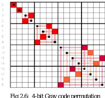
2.6.1 CONSTRUCTING AN n-BIT GRAY CODE
Fig 2.6: 4-bit Gray code permutation
The binary reflected gray code list for n bits can generated recursively from the list for n− 1 bits by reflecting the list i.e. listing the entries in reverse order, concatenating the original list with the reversed list, prefixing the entries in the original list with a binary 0, and then prefixing the entries in the reflected list with a binary 1. The one-bit Gray code is G1 = (0, 1). This can be thought of as built recursively as above from a zero-bit
Gray code G0 = { Λ } consisting of a single entry of zero length. This iterative process of
generating Gn+1 from Gn makes the following properties of the standard reflecting code clear:
1. Gn is a permutation of the numbers 0, 2n−1. Each number appears exactly once in the list. 2. Gn is embedded as the first half of Gn+1.
3.Therefore the coding is stable, in the sense that once a binary number appears in Gn it appears in the same position
in all longer lists; so it makes sense to talk about the reflective Gray code value of a number: G(m) = the m-th reflecting Gray code, counting from 0.
4. Each entry in Gn differs by only one bit from the previous entry. The Hamming distance is 1.
5. The last entry in Gn differs by only one bit from the first entry. The code is cyclic.
These characteristics suggest a simple and fast method of translating a binary value into the corresponding Gray code. Each bit is inverted if the next higher bit of the input value is set to one. This can be performed in parallel by a bit-shift and exclusive-or operation if they are available: the nth Gray code is obtained by computing
.
III. CONCLUSION
The attractive features of MTJ/PentaMTJ-based CMOS logic are low static power, short interconnect delay, and effective power gating because of nonvolatility. PentaMTJ-based logic decreases the area overhead by removing the intermediate circuitry needed for conversion of voltage to current or current to voltage. Moreover, no initial condition is required for performing the logic operation and self referencing property removes the extra MTJs used for referencing. PentaMTJ also provides guaranteed disturbance free reading and increased tolerance to process variations due to its differential nature.
REFERENCES
[1] Chappert.C, A. Fert, and F. N. Van Dau, “The emergence of spin electronics in data storage,” Nature Mater., vol. 6, no. 11, pp. 813–823, Nov. 2007.
[2] Deng.E, Y. Zhang, J.-O. Klein, D. Ravelsona, C. Chappert, and W. Zhao, “Low power magnetic full-adder based on spin transfer torque MRAM,” IEEE Trans. Magn., vol. 49, no. 9, pp. 4982–4987, Sep. 2013.
[5] Horowitz.P and W. Hill, The Art of Electronics. Cambridge, U.K.: Cambridge Univ. Press, 1989.
[6] Huda.S and A. Sheikholeslami, “A novel STT-MRAM cell with disturbance-free read operation,” IEEE Trans. Circuits Syst. I, Reg.Papers, vol. 60, no. 6, pp. 1534–1547, Jun. 2013.
[7] Lee.S, N. Kim, H. Yang, G. Lee, S. Lee, and H. Shin, “The 3-bit gray counter based on magnetic-tunnel-junction elements,” IEEE Trans.Magn., vol. 43, no. 6, pp. 2677–2679, Jun. 2007.
[8] Lyle et al.A, “Magnetic tunnel junction logic architecture for realization of simultaneous computation and communication,” IEEE Trans. Magn., vol. 47, no. 10, pp. 2970–2973, Oct. 2011.
[9] M. K. Gupta and M. Hasan, “Design of high speed energy efficient masking error immune PentaMTJ based TCAM,” IEEE Trans. Magn., no. 99. [10] Makarov.A, V. Sverdlov, D. Osintsev, and S. Selberherr, “Fast switching in magnetic tunnel junctions with two pinned layers: Micromagnetic modeling,” IEEE Trans. Magn., vol. 48, no. 4, pp. 1289–1292, Apr. 2012.