http://dx.doi.org/10.4236/jemaa.2016.82003
How to cite this paper: Khudaverdyan, S., Hovhannisyan, T., Meliqyan, N., Mehrabyan, N., Tsaturyan, S., Khachatryan, M. and Vaseashta, A. (2016) On the Model of Spectral Analysis of Optical Radiation. Journal of Electromagnetic Analysis and Applications, 8, 23-32. http://dx.doi.org/10.4236/jemaa.2016.82003
On the Model of Spectral Analysis of Optical
Radiation
Surik Khudaverdyan1*, Taron Hovhannisyan1, Nazeli Meliqyan1,
Narine Mehrabyan1, Stepan Tsaturyan1, Mane Khachatryan1, Ashok Vaseashta2 1Armenian National Polytechnic University, Yerevan, Armenia
2Norwich University Applied Institutes, Herndon, USA
Received 8 January 2016; accepted 22 February 2016; published 25 February 2016
Copyright © 2016 by authors and Scientific Research Publishing Inc.
This work is licensed under the Creative Commons Attribution International License (CC BY).
http://creativecommons.org/licenses/by/4.0/
Abstract
A silicon photodiode structure was studied for the spectral analysis of optical radiation. The struc-ture consists of oppositely-directed barriers. We developed a model of the electronic processes oc-curring in the structure. The possibilities of the selection of separate waves from the integral flux of radiation, the wave absorption and the quantitative spectral analysis of the waves of the model for contaminated environment were investigated. An algorithm was developed for carrying out the spectral analysis without the preliminary calibration, and for promoting a possible creation of a new type of a portable semiconductor spectrophotometer.
Keywords
Spectral Analysis, Monitoring, Photosensitivity, Photodiode
1. Introduction
The environmental crisis, as it relates to interaction between humans and the nature seems to be worsening with the progression of time. Depletion of ozone layer, acid rains, radioactive pollution, climate changes are some of the consequences on the environment. The environment is further burdened by mining, growing transportation and intentional activities as a result of global terrorism and poses some of the most precarious consequences. One of the most vulnerable problems is the pollution of fresh water with petroleum products, phenols, nitrogen, pesticides and heavy metals. Therefore, as scientists, an important task is to develop a large-scale real time mon-itoring of the water quality and the environment [1]-[3].
obtained by light filters, a prism, a diffraction grating and high accuracy mechanical devices [4]. The spectro-photometric systems like this are not multi-purpose and require additional devices and external software support for the fulfillment of every new function. As a result, they are quite expensive and are little fit to be used in field conditions.
The effective solution to the above-stated problems is the development of such a semiconductor structure in which the electronic processes will provide high accuracy spectral analysis of the electromagnetic radiation.
There is research done in the area of multicolored photo receivers [5]-[13] in which multilayer structures or a cascade chain of active layers with different base thicknesses are used. In such photo receivers, the different pe-netration depths of individual waves of the radiation provide different degrees of photoconductivity. The ma-thematical modeling of the measurement results provides information on the spectral distribution of the intensity.
The registration accuracy of the above-mentioned structures is due to the necessity to provide similar absorp-tion condiabsorp-tions and to create multiple photodiodes and multilayer structures with nanometric accuracy. The complicated technology of the development and the impossibility to control the spectral sensitivity by the exter-nal voltage impedes their development and usage.
To solve the problem, we propose a cheap, small-size, multi-functional primary sensor. In research papers
[14][15], we conducted feasibility studies of creation of the spectral selective sensitivity in parallel placed pho-todiode structures and vertically placed double-barrier structures. Both structures consist of a Schottky barrier and n-p junction which is electrically oppositely-directed. We demonstrate that in such structures, with the help of an appropriate algorithm, it is possible to select and register individual electromagnetic waves and their inten-sities from the integral flux of radiation by changing the external voltage. This investigation is also useful in optical communication, study of microbiological systems, medical objects, and for environmental protection, just to name a few applications [16]-[19].
2. The Object under Study
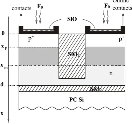
The research work covers the modeling of the electronic process of the spectral analysis with the help of an electrically oppositely-directed silicon photodiode structure (Figure 1), and feasibility studies of spectrophoto-meter of such a process. The planar structure allows us to direct the radiation onto the sensitive surface of two parallel distributed diodes. In the structure under investigation, the photodiodes participating in the creation of the photocurrent, are independent with respect to the photoelectronic processes occurring in them (Figure 1). Their influence on one another is regarded as external influence.
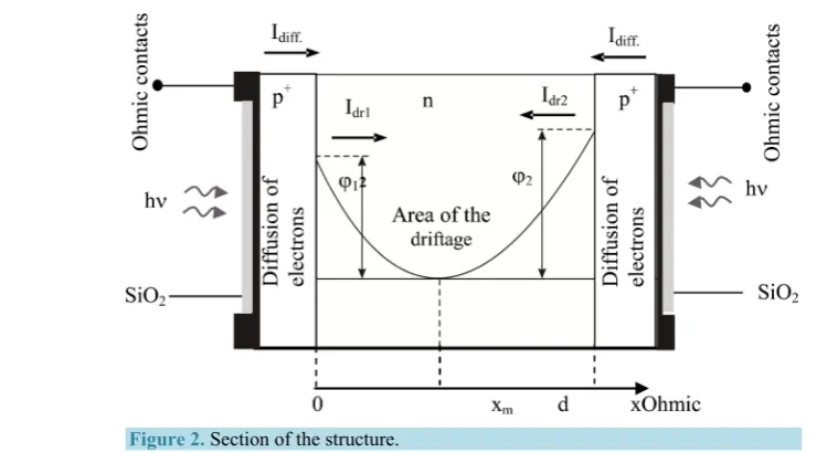
[image:2.595.198.428.490.707.2]In Figure 2, the potential barriers of the diodes are oppositely directed. Increase of one of the depleted layers, along with decrease of the other layer by the external voltage ensures the different efficiencies of radiation ab-
Figure 2.Section of the structure.
sorption along with the wavelength. The channels are electrically connected by a high conductivity p+ layer. The surface SiO2 film is reflective and is placed on the semitransparent metal film. The interior SiO2 film sepa-rates the upper active layer from the interior polycrystalline silicon passive platform. The latter transmits the unregistered part of the deeply penetrated radiation. At any polarization of the voltage, one of the n-p junctions is biased in the forward direction, and the other junction is biased in the opposite direction. The oppositely di-rected potential barrier gets wider with the increase of the bias voltage at the expense of the high ohmic n-layer. P+ layer is thin and the thickness d of the structure depends mainly on the n-layer, and in the point xp the radia-tion intensity is taken to be equal to the surface intensity F0.
Considering that the base is covered by the depleted regions of both barriers, we determine the distribution of the potential in the spatial charge region of the double-barrier structure (Figure 2). For that, we solve the Poisson equation which connects the field potential V x
( )
with the volume density of the charges creating that field,( )
2
2
0
d
, d
V x x
ρ εε
= − (1)
In Poisson equation we pass from the potential V x
( )
on to the potential energy of electrons ϕ( )
x ,( )
( )
(
ϕ x = −qV x)
. Since ρ =qNd, we obtain,2 2
2 0
d ,
d d
N q x
ϕ εε
= (2)
where Nd: the concentration of donor impurities; ε: the relative dielectric permeability of the substance; ε0: the dielectric permeability of the vacuum and q: the electron charge.
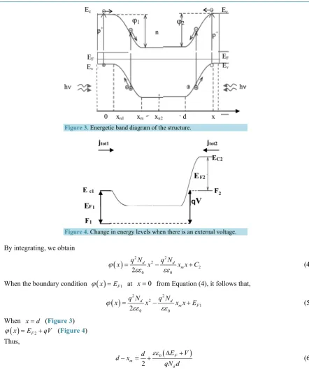
The boundary conditions for the given equation are d 0 dx
ϕ
=
at x x= m (Figure 2, xm is the minimum
of the potential energy of electrons) and ϕ
( )
x =EF1 at x=0 (Figure 3,Figure 4). Taking into account the boundary conditions, we integrate Equation (2) and obtain,2 2
2
2 1
0 0
2 d d
F q N q N m F
E +qV= εε d − εε x d E+
( )
21 0
d
d d
x q N x C
x ϕ
εε
= + , 1 2
0
d m
q N C = − εε x
( )
2(
)
0
d
dxx q Nd x xm
ϕ
εε
Figure 3.Energetic band diagram of the structure.
Figure 4.Change in energy levels when there is an external voltage.
By integrating, we obtain
( )
2 2 22
0 0
2 d d m
q N q N
x x x x C
ϕ
εε εε
= − + (4)
When the boundary condition ϕ
( )
x =EF1 at x=0 from Equation (4), it follows that,( )
2 2 21
0 0
2 d d m F
q N q N
x x x x E
ϕ
εε εε
= − + (5)
When x d= (Figure 3)
( )
x EF2 qVϕ = + (Figure 4)
Thus,
(
)
0
2 F
m
d
E V
d d x
qN d
εε ∆ +
− = + (6)
where: ∆EF =EF2−EF1.
If both barriers are identical, then EF2−EF1=0. Consequently:
0 2 m
d
V d d x
qN d
εε
− = + (7)
0 0 2 d V d qN d εε + =
When 1015 см3
d
N = − , d = ×2 10−4см it follows, 2
0
3 2d
qN d V = − εε = − V
With the help of (7) we can determine the modulation depths of depleted layers, and the position of xm:
0 2 m d V d x qN d εε
= −
(8)
And with the help of ∆xm=xm2−xm1 we can determine the wavelength and the intensity of the absorbing radiation. For that we first determine the total photocurrent flowing through the structure.
In certain diodes, the photocurrent has diffusion and drift components. To determine the diffusion photocur-rent, it is necessary to find pn density of minority charge carriers—holes, in the n-base. For that, the following one-dimensional diffusion equation is solved,
( )
2
0
2n 2n 2n ,
p
p p
G x
p p p
D
x L L
∂
− = − −
∂ (9)
where Lp = Dp pτ : the diffusion length of holes in the n-region; G x
( )
=F0αe−αx: the generation rate of electron-hole pairs; F0: the total flux of incident photons; α: the absorption coefficient of electromagnetic rad-iation; Dp: the diffusion coefficient of holes in the n-region; τp: the excess-carrier; lifetime: hole lifetime in then-region; pn0: the equilibrium density of holes in the n-region.
Equation (9), at the boundary conditions of pn = pn0 when х = ∞ and pn = 0 when х = xn, can be solved as fol-lows.
The relevant homogeneous equation considered is 2
2n 2n 0 p p p x L ∂ − = ∂ 2 2 1 0 p k L
− = for which is a characteristic equation with the roots 1 1
p
k L
= and 2 1
p
k L
= − . Since k1≠ k2, the
general solution for the homogeneous equation will be pn1 C1e x Lp C2ex Lp
−
= + , where C2=0, since at х= ∞,
pn1= ∞, and it has no physical interpretation. Hence
1 1e x Lp
n
p =C −
. (10) The specific solution of Equation (9) should be found in terms of the product e−αx and the polynomial with unknown coefficients. That is
2 e x
n
p =A −α +B (11) where the coefficients A and B of Equation (11) are determined by the method of undetermined coefficients. For that, Equation (3) is differentiated, and as a result we obtain:
e x n p A x α α − ∂ = − ∂ ; 2 2 2 e x n p A x α α − ∂ =
∂ (12)
If we substitute the values (3) and (4) into the given Equation (1), we will obtain:
2 0 0
2 2 2
e x e x e x n
p
p p p
F p
A B
A
D
L L L
α α α α
α − − − − = − − −
2 0 2 1 p p p L F A D L α α − = − ,
(
)
2 0 2 2 1 p p p L F A D L α α = − , 0 2 n2p p
p B
L = L , B p= n0. Thus Equation (11) takes the form:
(
)
2 0
2 0 2 2 e
1 p x n n p p L F p p D L α α α − = + −
(13) The general solution for Equation (9), taking into account (10), will be
(
)
2 0
1e 0 2 2 e
1
n p
x L x
n n
p p
L F
p C p
D L α α α − − = + + −
C1 is determined from the boundary conditions pn= 0 when x = xn, that is:
(
)
2 0
1e 0 2 2 e
1
n p n
x L x
n p p L F C p D L α α α − = − − − − Hence
(
)
2 01 0 2 2 e e
1
p n x L
p x n p p L F C p D L α α α − = − + −
As a result, for the densities of minority charge carriers in the n-region of the semiconductor and the diffusion current, we will obtain the following equalities:
(
)
(
)
2 2
0 0
0 0 2 2 2 2
e e e 1 1 n p n x x x L
p x p
n n n
n p p p
L L
F F
p p p
D L D L
α α α α α α − − − = − + + − − , 2 2
0 0 0
2 2 2 2
e
d e e
d 1 1
n
n p
x
x x L
p n p p x
n
pдиф p
p p p
D qp q L F qF L
p
j qD
x L L L
α α α α α α − − − = = + − − − .
At the point x = xn
, 0 p 01 p e xn
p dif n
p p
D L
j qp qF
L L
α
α
α −
= +
+ (14) The density of the drift current has the form: jdr =qF0
(
1 e− −αxn)
. The photocurrent for each diode is determined by the sum of the diffusion and drift components. 0e xn 1 p 1 0 0 p
tot dr p dif n
p p
L D
j j j qF qF qp
L L α α α − = + = − + + +
(15)
Under normal operating conditions, the member containing pn0 is significantly smaller than the first member, and it can be neglected.
Accordingly, the drift current for two diodes in the ranges of the potential barriers with the widths xn1 and 2
n
x will take the form
(
1 e n1)
,(
1 e n2)
dr dr
x x
p o p o
j =qF − −α j =qF − −α (16)
Since the p+ layer is very thin, the absorption depths are taken to be equal to the widths of the depleted layers of photodiodes xn1= xm and xn1 = d-xm(Figure 2), and are defined by the following expressions (7) and (8).
Finally, expression (15) without the diffusion component will take the following form for the general photocurrent flowing through one barrier.
1 e 1 1 n dif dr x
tot p p o
p
j j j qF
L α α − = + = − +
The difference of the photocurrents of two barriers will give the general photocurrent flowing throught the structure.
2 1
e e
1
n n
x x
o
p
j qF
L
α α
α
− −
−
=
+
(18)
At the illumination by the integral flux of radiation, expression (18) will take the following form.
2 1
e e
1
i n jx i n jx
totij oi
ij ij i p
j q F
L
α α
α
− −
−
=
+
∑
∑
(19)
where (i=1,2,3,) changes with the change of the radiation wavelength in the integral flux, and ( j=1,2,3,) changes with the change of bias voltage, F(λi)—the total flux of photons incident along the wavelength ∆λi.
At the application of the negative voltage to the right-side barrier (minus is applied to the right contact), the right p-n junction is biased in the opposite direction. As a result, the potential barrier gets wider (Figure 3), the absorption capacity of some wave range ∆λ grows, and, consequently, grows the photocurrent I2 is conditioned by right-side barrier.At the same time, the left-side barrier of the n-p junction gets narrower, and the absorption capacity of the range ∆λof the adjacent region and the photocurrent I1conditioned by the n-p junction decrease. With the help of the algorithm as stated, it is possible to register a separate wavelength λi and its intensity by changing the voltage ∆V, thus obtaining the spectral dependence for wave intensities.In the research we used the AM0 spectral distribution of the solar radiation covering the wavelengths from λ = 200 nm up to λ = 800 nm. With the increase of the wavelength, we observe the increase of the intensity [20]. It brings to the spectral growth of the absorption depth, and allows us to successively register the waves via widening the absorption en-vironment from the depth towards the surface. Experiments were carried out on the Si built photodetector (Figure 5). Photosensitivity region is of 400 nm to 1100 nm.
The linear dependence of the current and the wave intensity in expression (18) allows us to reduce the spectral intensity and, thus, to comply the absorption depth of the waves with the depth of the registering environment. Under the conditions of the reduction of the solar spectrum for 1010 times, according to Lambert’s law, the spectral dependence of the absorption depth in the shortwave (Figure 6(a)) and the long wave (Figure 6(b)) ranges, reaches from 20 nm up to 16 μk. The most intensive growth of the depth is observed in the ranges higher than 400 nm (Figure 6presents the range from 100 nm up to 16 μk). Thus, the contribution of the waves into the current in that range is relatively small.
Now, let us consider some peculiarities of the selection of separate waves from the integral flux of radiation with the help of the oppositely directed diode structures, and find out the possibilities of detection of the required wavelength and its intensity under the conditions of the wave absorption and the wave emission (fluorescence) by the object.
3. Results of the Research
[image:7.595.251.375.617.703.2]For determination of the spectral composition of the integral flux of the electromagnetic radiation and the defini-tion of its change, the radiadefini-tion absorpdefini-tion of the Sun is investigated. The wave intensities of the radiadefini-tion are equally reduced so that the absorption depth corresponds to the width of the registering environment (1 - 2 μm). The photocurrent corresponding to the biggest possible value of x is conditioned by the most deeply penetrated wave. Under these conditions, the process of the selection of separate waves and their intensities from the integral flux of radiation consists in the following:
Let us assume that the informative signal is the photocurrent. We have the biggest values xm1 and xm2 of xm corresponding to the change of bias voltage 1 mV, and the relevant photocurrents I1 and I2. They are obtained from the absorption of the most deeply penetrated wave λi. With the help of these photocurrents, from Lambert’s law on radiation absorption in the homogeneous environment, we will have the coefficient of wave absorption.
2
1 1 ln i x II α =
∆ (20) where ∆ =x xm2−xm1.
Then, with the help of α = f
( )
λi [21] and with the corresponding program we can determine the length ofthe wave for the initial material of the photodetector, e.g. for silicon. By means of the formula for the photocur-rent (18), we will obtain the intensities of separate waves in the absorbed radiation.
2 1
e e
1
i n i n
i
oi x x
i p
j F
q
L
α α
α
− −
=
−
+
(21)
Thus, with the help of (8), (20) and (21), we determine the absorption coefficient of the most deeply pene-trated wave, the wavelength and the intensity of the wave.
Then, with the help of expression (18), considering the absorption surface, we form the dependence I1 = f(V) and subtract it from the experimental dependence I = f(V)of the summed current. As a result, we obtain a new dependence of the summed photocurrent on V, without the dependence I1 = f(V). By means of relevant software, this method helps us successively determine the lengths and the intensities of all the waves in the radiation, and, finally, the following dependence for the radiation spectrum (Figure 7).
[image:8.595.91.532.366.536.2](a) (b)
Figure 6. Dependence of the absorption depth from wavelength. For the short-wavelength range (a). For the long- wavelength range (b).
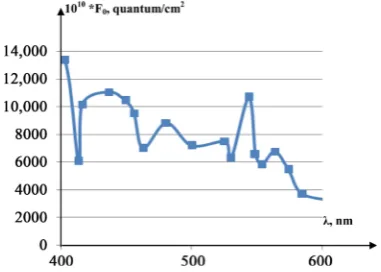
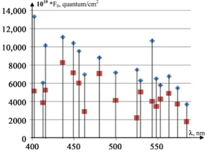
[image:8.595.218.409.572.708.2]Figure 8. The change of the spectral distribution of the radiation intensity.
It can be kept in the memory of the device, and be applied in the process of the object identification. The mainparameters of the quantitative determination of hazardous substances in water by means of UV and visible spetroscopy are known [7][8]. With the help of these parameters, for the identification of hazardous substances in water and the risk reduction, the change of the spectral composition was determined. For ten wavelength sit is brought in Figure 8.
4. Conclusion
1) A new model of the portable photo sensor is developed for the remote identification of optical information. Identification and quantitative analysis of hazardous substances in water is studied as well.
2) In the radiation spectrum, the waves have different absorption depths, and the process of the selection of waves is carried out via the gradual change of the external voltage applied to the structure, and the widening of the registering volume.
3) The algorithm developed here permits us to carry out the spectral analysis without any preliminary calibra-tion.
References
[1] Jiang, P., Xia, H.B., He, Z.Y. and Wang, Z.M. (2009) Design of a Water Environment Monitoring System Based on Wireless Sensor Networks. Sensors, 9, 6411-6434. http://dx.doi.org/10.3390/s90806411
[2] Normatov, P.I., Armstrong, R., Normatov, I.S. and Narzulloev, N. (2015) Monitoring Extreme Water Factors and Studying the Anthropogenic Load of Industrial Objects on Water Quality in the Zeravshan River Basin. Russian
Mete-orology and Hydrology, 40, 347-354. http://dx.doi.org/10.3103/S106837391505009X
[3] Vaganov, M. (2012) The Parallel Spectrum Analyzer of Optical Signals. Saint-Petersburg State University of Aero-space Instrumentation Saint-Petersburg, Russia, 1-5. http://guap.ru/guap/nids/pdf_2012/vaganov.pdf
[4] Pshinko, G.N., Kobets, S.A. and Puzyrnayain, L.N. (2013) Concentration of U(VI) on a Complexing Sorbent for Its Determination by the Spectrophotometric Method. Journal of Water Chemistry and Technology, 35, 145-151.
http://dx.doi.org/10.3103/S1063455X13040012
[5] Kautzsch, T. (2013) Photo Cell Devices and Methods for Spectrometric Applications. US Patent No. 20130285187 A1. [6] Kautzsch, T. (2014) Photodetector with Controllable Spectral Response. US Patent No. 8916873 B2.
[7] Kautzsch, T. (2012) Photocell Devices and Methods for Spectroscopic Applications. Patent DE 102013207801 A1. [8] Jan, C., Daniel, P., Man, S.T. and Univ, N. (2005) Photodetector with Controllable Spectral Response. US Patent No.
8916873 B2.
[9] Nataša, G. and Novel, A. (2007) Type of Tri-Colour Light-Emitting-Diode-Based Spectrometric Detector for Low- Budget Flow-Injection Analysis. Sensors, 7, 166-184. http://dx.doi.org/10.3390/s7020166
[10] Seymour, E.Ç., Freedman, D.S., Gökkavas, M., Özbay, E., Sahin, M. and Ünlü, M.S. (2014) Improved Selectivity from a Wavelength Addressable Device for Wireless Stimulation of Neural Tissue. Frontiers in Neuroengineering, 7, 1-12.
http://dx.doi.org/10.3389/fneng.2014.00005
Sten-nis Space Center, Mississippi, Refer to SSC-00072.
[12] Vanyushin, I.V., Gergel, V.A., Zimoglyad, V.A. and Tishin, Y.I. (2005) Adjusting the Spectral Response of Silicon Photodiodes by Additional Dopant Implantation. Russian Microelectronics, 34, 155-159.
http://dx.doi.org/10.1007/s11180-005-0024-5
[13] Vanyushin, I.V., Gergel’, V.A., Zimoglyad, V.A., Lependin, A.V. and Tishin, Yu, I. (2006) Profiling the Boron Dis-tribution in Asymmetric n+-p Silicon Photodiodes and a New Concept for Creating Selectively Sensitive Photocells for
Megapixel Color-Image Receivers. Physical Processes in Electron Devices, Journal of Communications Technology
and Electronics, 51, 1425-1430. http://link.springer.com/article/10.1134%2FS106422690612014X#/close
[14] Khudaverdyan, S., Khachatryan, M., Khudaverdyan, D., Tsaturyan, S. and Vaseashta, A. (2013) New Model of Spec- tral Analysis of Integral Flux of Radiation. In: Khudaverdyan, S. and Vaseashta, A., Eds., NATO Science for Peace and
Security Series B: Physics and Biophysics,Springer, Netherlands, 261-269.
[15] Khudaverdyan, S., Avetisyan, A., Khudaverdyan, D. and Vaseashta, A. (2013) Photoelectric Properties of Selectively Sensitive Sensors for the Detection of Hazardous Materials. In: Khudaverdyan, S. and Vaseashta, A., Eds., NATO
Science for Peace and Security Series B: Physics and Biophysics, Springer, Netherlands, 183-191.
http://dx.doi.org/10.1007/978-94-007-7003-4_15
[16] Khudaverdyan, S., Petrosyan, O., Dokholyan, J., Khudaverdyan, D. and Tsaturyan, S. (2012) Modeling of a New Type of an Optoelectronic Biosensor for the Monitoring of the Environment and the Food Products. In: Vaseashta, A., Braman, E. And Susmann, P., Eds., NATO Science for Peace and Security Series A: Chemistry and Biology, Springer, Netherlands, 179-184. http://dx.doi.org/10.1007/978-94-007-2488-4_17
[17] Bornman, J.F., Barnes, P.W., Robinson, S.A., Ballaré, C.L., Flinte, S.D. and Caldwellf, M.M. (2015) Solar Ultraviolet Radiation and Ozone Depletion Driven Climate Change: Effects on Terrestrial Ecosystems. Photochemical &
Photobi-ological Sciences, 14, 88-107. http://dx.doi.org/10.1039/C4PP90034K
[18] Han, J.H., Goun Jo., Y., Kim, J.C., Lee, J.-B., Kim, Y.-C., Kang, H. and Hwang, I.-W. (2016) Contrast Agent Free Detection of Bowel Perforation Using Chlorophyll Derivatives from Food Plants. Chemical Physics Letters, 643, 10- 15.
[19] Meichtry, J.M., Colbeau-Justin, C., Custo, G. and Litter, M.I. (2014) TiO2-Photocatalytic Transformation of Cr(VI) in the Presence of EDTA: Comparison of Different Commercial Photocatalysts and Studies by Time Resolved Microwave Conductivity. Applied Catalysis B: Environmental, 144, 189-195.
http://dx.doi.org/10.1016/j.apcatb.2013.06.032
[20] http://www.pveducation.org/pvcdrom/materials/optical-properties-of-silicon