ISSN: 1992-8645 www.jatit.org E-ISSN: 1817-3195
IMPROVING THE EFFICIENCY OF MULTI-COLOR LEDS
DISPLAY SYSTEM USING THE IMPROVED PWM
TECHNIQUE ON FPGA.
K. MATEUR1, R. ELGOURI1,2, M. ALAREQI1,3,
A. Mezouari
1, H. Dahou
1, L. HLOU1.1
Laboratory of Electrical Engineering & Energy Systems Faculty of Science Ibn Tofail University, Kenitra, Morocco
2
Laboratory of Electrical Engineering and Telecommunications Systems, National School of Applied Sciences (ENSA), Ibn Tofail University,
Kenitra, Morocco
3
Community College, Sana'a, Yemen
Corresponding author E-mail: [email protected]
ABSTRACT
Light Emitting diode (LED) video displays are future of large-area display market. Their scale, their durability and their ability to produce an attractive video in ambient light conditions, make them the favorable screens in all display systems. To increase the light quality of LED displays, it is necessary to improve the techniques that control the light variations while keeping stable energy consumption. This technique has become a major objective in the design of such displays systems. This paper presents a comparative study between two techniques to control brightness levels of LED displays, the first technique controls by varying direct current amplitude (DC), the second by varying the duty cycle of the current square wave with fixed amplitude (PWM). The paper also proposes an improved PWM solution, which is based on the approximation of the PWM curve to the DC curve in order to have the luminous efficiency as the last one. The demonstration is presented as a serial of mathematical calculations to choose the intermediate point and build low-cost hardware algorithm for this new method. The performance of this method is studied experimentally using the FPGA design and is compared with the PWM method.
Keywords: LED, Display systems, Display driver, PWM, FPGA, Grayscale, multiplexing LEDs,
1. INTRODUCTION
Developments, industrial and commercial, have increased exponentially in recent years [1]. With this development, the technology has been able to facilitate multiple services by exploiting the different types of energy sources, but on the other hand this development increased the energy consumption in the world. Based on data from the US Department of Energy, approximately 30% of the electric power has been consumed by the commercial and industrial lighting [2]. Reducing the power dissipated by the lighting is then a major factor in saving energy. Therefore, studies on improving these systems and the lighting energy savings deserve more attention from academic researchers.
LED screens have large big of the market for large area display. Their scale, their durability, their ability to produce an attractive video and their low power consumption, make this technology favorable than other display systems.
wide range of applications including stadiums, arenas, a complex of entertainment, etc [3]. Using PWM technique to control the luminous of RGB LED and reduce energy consumed using DC technique (converter digital to analog) in these large-area displays, caused an error gap between color levels produced by these two techniques. The main objective in the design of display systems is to improve luminous efficiency by reducing this error gap, maintaining stable the cost and the energy consumption of these systems. For this, the methods of controlling the brightness of each LED in the display matrix still needs improvement in order to increase the light quality without instability in energy consumption in the entire system.
ISSN: 1992-8645 www.jatit.org E-ISSN: 1817-3195 On other hand, the optical characteristics of RGB
LEDs on this display system remain unknown. The practical uses luminous control techniques for each component R, G or B of RGB LEDs still need improvement.
This paper presents an efficient design of an RGB LEDs display system controller by improving the performance of the luminous dimming method of each RGB color component. This design replaces variation of direct current amplitude DC by variation PWM while changing its characteristic (current-luminous) by increasing its variation range.
This paper is organized as follows; the first section introduces the LED display structure and luminous control methods of each LED. The second section describes the approach of the improved PWM method and the performance compared to DC and simple PWM methods. Simulation and experimental results are presented and discussed in section 3. Finally, the paper ends with a conclusion.
2. CONTROL METHODS OF COLOR LUMINOUS.
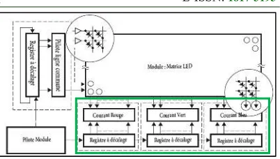
LED multicolor large-area display systems require a complex treatment that requires high performance conditions. Using the multiplexing technique (Fig. 1), the display driver can manage a large number of tri-color LEDs RGB organized in the form of matrices.
This method allows to scan all the LEDs and assigning to each color component (r, g and b) the level of corresponding brightness. This operation requires a very high speed in the order of KHz so that the human eye cannot distinguish the fluctuations of the image [5]. Therefore, it is very important to design an efficient display driver. In particular, the efficient method of assigning information of each pixel to the corresponding LED (part bordered by the green color in Fig. 1). This operation affects directly the energy efficiency of the display as well as the quality of the displayed image. In this sense, several studies have been done on these methods [6] [7] [8]. In general, they can be divided into two main categories:
[image:2.595.308.509.80.194.2]• Analog or direct current (DC). • Pulse width modulation (PWM). •
Fig. 1 : The multiplexing method of an LED matrix RGB.
The first method controls luminous by varying the amplitude of a DC current (AM variation technique). It can be obtained based on the principle of the digital to analog converters. This principle is done by varying a variable resistor in order to affect a current level corresponds to the desired illumination of the LED [9]. The analog control provides higher luminous efficiency and stability of the color variation [8].
However, this method has two weaknesses first one energy consumed by these converters cause the interference electromagnetic, secondly the intrinsic optical properties of the LEDs which the output varies non-linearly with the DC current variation, this method is suitable for lighting applications that do not require linear variation [10].
a. Pulse Width Modulation Algorithme
The problem associated with the DC method is satisfied when the PWM method is used. By this approach, the energy consumed by the analog digital converters is preserved by replacing these DACs by a constant direct current in the form of a square signal of period T and duty cycle t/T. By exploiting the very fast response time of the LEDs which can be controlled by using succession of current pulses, This current flows through the LEDs for a duration of the pulse '1' (tFig. 2), and completely extinguishes them for the duration (T-t in Fig. 2). For example, the current pulse with a period T of 1s (frequency 1Hz) with a duty cycle of 50% and current with amplitude of 2A has the same effect as a driving current of 1A in terms of brightness [9] (Fig. 2).
ISSN: 1992-8645 www.jatit.org E-ISSN: 1817-3195
Fig. 2 : Current Signal Formats for PWM Technique
[10].
In addition to the linear variation, the PWM method is also intrinsically compatible with the operation of the display systems. The LED Luminous is controlled directly from the brightness information embedded in the digital input signal. This information can be corresponding to the time t of the Pulse '1' of the PWM signal as showing in Fig. 2.
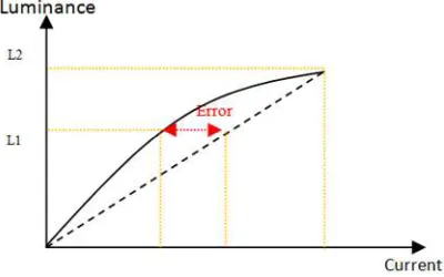
The disadvantage of the PWM method is that it produces a reduced luminous of the LEDs than DC method, for example the luminance PWM for a current value I1 is less than that of DC (Fig. 3).
Fig. 3 : The curves associated with two methods of variation of the luminous intensity of the LEDs.
b. Hardware Description of PWM
In the driver design process, there are two methods for performing the PWM technique: the counter comparison method [9] and the method of separating bit planes according to weight. The first method generates an initial value of 0 and its maximum value is 255, the counter continues counting according to the clock cycles. The initial state of the LED is set to '1'. During the next clock cycle, the data (0-255) read is compared with the counter data, if the read data is greater than the value of the counter, the conduction time of the pixels is not sufficient.
Therefore the LED must remain in state '1', if the data is less than the value of the counter, the
conduction time of pixels complies with the requirements. Therefore the LED goes from state '1' State '0'. In practice, for this approach to read the data and compare it 256 times for each frame and if the screen is slightly larger, it is necessary to have a very fast speed to have a flicker-free display [11][12], which is a disadvantage of this method.
For the second method, only one bit of the digital signal is displayed among the eight data bits (D7 - D0), and the signal can be displayed 8 times to present all eight bits of data except that the bits must take the different durations according to the weight of each of them as illustrated in Table 1.
[image:3.595.307.505.311.445.2]The corresponding light intensity is the sum of the bits which have the state 1.
Table 1 : The current intensity variation by the PWM method.
Bit of data Duty cycle (t/T)
8th Bit 128/255 7th Bit 64/255 6th Bit 32/255 5th Bit 16/255
4th Bit 8/255
3th Bit 4/255
2nd Bit 2/255
1st Bit 1/255
At RGB component data of each pixel, for each bit '1' corresponds a cyclic ratio t/T according to their weights (D7, D6, D5, D4, D3, D2, D1, and D0).
The conduction time given to the low luminosity is short, while the conduction time given to the high luminosity is long. Thus, the full cyclic ratio of the 8-bit data can be calculated by the sum of the cyclic ratios of the values of '1'.
c. Display control adapted to the PWM method
[image:3.595.87.287.374.499.2]ISSN: 1992-8645 www.jatit.org E-ISSN: 1817-3195
Fig. 4 : Typical LED driver module [13].
The FPGA circuit continues to transmit serial data until all shift registers are populated with data bits (Di). When the transmission of all the data bits
corresponding to Di is completed, the signal LAT
will be activated to lock the transmission of the data bits and to pass to the next data bits Di+1. The
current-constant LED drivers are then activated by lowering the BLANK signal for a duration corresponding to the weight of the stored data bits. The same process is repeated until all eight groups of data bits (representing the eight different weights) are transmitted to the LED driver modules. After this value input to the row decoder, the counter corresponding to the ABCD inputs is incremented by 1 to select the next row, transmission of the data bits for that row will begin and the LEDs of the pixels will be activated in a manner similar to the first one.
[image:4.595.305.506.543.719.2]A typical example of a timing diagram corresponding to this operation is shown in Fig. 5.
Fig. 5 : Timing diagram showing the various control signals applied to the LED control module.
3. PROPOSING METHOD TO IMPROVE PWM
produce the same luminance as the originally DC current. These simple calculations are based on the slopes m1 and m2 of the two linear portions of
each section (ON) and (NM) as shown in figure Fig. 6. Consider the continuous variation curves of an LED, which can generally be approximated by equation (1) to a quadratic form.
(1) ∗ ∗
Where ‘x’ and ‘y’ represent respectively duty cycle (coded on 8 bits) and standardized luminosity (y=L/Lmax) equivalent to the applied
technique. The coefficients ‘a’ and ‘b’ can be obtained by performing a curve fitting to the DC gradation obtained from an experiment (example next section).
Assuming that the original signal has a PWM duty cycle of 'x', the normalized luminance 'y' corresponding to the PWM technique is expressed by equation (2):
(2) /
[image:4.595.89.293.544.657.2]ISSN: 1992-8645 www.jatit.org E-ISSN: 1817-3195 PWM duty cycle value is in the lower part of the
linear section (ON) with a slope m1. Then the
current PWM will have a duty cycle PWM equivalent to x' calculated by the equation (3).
(3) ∗
If L ≥ L1, the linear section is in the upper part
(line (NM) with slope m2). The PWM duty cycle
equivalent to their current can be calculated from equation (4).
(4) ∗
Using the DC curve approach, conversion can be done more easily using equation (5), assuming that the DC variation curve has been approximated by the two combined linear sections.
(5) ∗ ∗ ∗ ∗ ∗
a. The intermediate point of luminous efficiency I1 (x1, y1).
The concept of "luminous efficiency" is used here to reflect the fact that the light emitted by LED continuously changes during the display of the images and it is assumed that the LEDs have the same probability of operating at any point on the variation curve.
As illustrated in la Fig. 6, the task is equivalent to maximizing the area between points O, N, M and F (ONMF). This surface is calculated by equation (6) if we take y2 is
maximum luminance which corresponds to x2 in
point M:
(6) ∗ ∗ ∗ ∗
The values y1 and y2 are replaced by their corresponding values according to equation (1):
(7) ONMF ∗ a ∗ x ∗ x x ! x ∗
I ∗ b ∗ x
To determine the x1 which maximizes the ONMF
area, the derivative of ONMF with respect to x1 is
set to 0, which gives equation (8):
(8) $ ∗ $
The result is independent of the coefficients of the quadratic function; it is also applicable to all types of LEDs which have a luminous output characteristic.
In fact, the result remains valid even for the case
function y = b * x, in which case the improved PWM method will have the same performance as the PWM method, There will be no gain in luminous efficiency.
b. The hardware description of improved MPW algorithm.
To achieve the improved PWM method on LED display systems based on the module shown in Fig. 4, the reference current IRef can be divided to
two same intensity current INRef (with INRef=IRef/2).
The INRef can be ussed as an intermediate point
between 0 and IRef=2*INRef as shown in Fig. 7.
Affectation of both of these currents will be controlled directly by the FPGA driver. Indeed, the first driver is configured to deliver a maximum current of INRef to the LED pixels.
Therefore, the use of second parallel current provides a maximum current of I2 = 2 * IRef to be
delivered to the LED pixels.
To control with this method, the FPGA driver separate the originally data (8-bits of pixel) to two buses for controlling the value of each INRef. For example, considering that the required intensity level of a given pixel component is represented by the 8-bit signal: [10100000]. If a single LED control module with IRef is used, the average
current Ip delivered to the LED pixel will be calculated according to the following equations:
(9) %& ' ( %)*+,
(10) %& %)*+, ' ( %)*+,
Equation (10) means that the same average current the 8-bit signal: [1010 0000] can be obtained using direct constant current INRef and
LED driver module (with INRef). The first
equivalent to 255/255 = [11111111], and the other with the binary equivalent of 65/255 = [01000001].
Based on the above example, if ‘x’ is equal to the decimal equivalent of the 8-bit signal for a pixel component, the equivalent signal can be converted into two sub-signals 8-bit consisting of the following:
If x ≥ 128: the IP equal to INRef plus [binary
equivalent of 2*x-255].
If x <128: the IP equal to [binary equivalent of
2*x].
ISSN: 1992-8645 www.jatit.org E-ISSN: 1817-3195
Fig. 7 : Using the paralleling of two drivers to have three levels of currents.
The proposed structure can reach more than two current levels, if this method finds recognition and adoption on the part of the LED display industry in the future. Integrated circuits containing several control units can be manufactured to achieve better brightness with only a small increase in the cost of the equipment.
4. EXPERIENCE, RESULTS AND DISCUSSION
In order to demonstrate the feasibility of the algorithm proposed, an experiment was carried out as a hardware architecture using Xilinx’s ISE (Integrated Software Environment), synthesized on a single Xilinx’s and implemented in Nexys2 Digilent card based on the spartan3e XC3S500E
[image:6.595.314.497.172.261.2]FG320 FPGA circuit which contains about 500k logic gates and which can be manipulated with a processing speed of 50 MHz adapted to the design of LED display system [14]. As shown in Fig. 8, this card contains several communication devices (PS / 32, Hi-speed, Pmod, VGA port, RS232, FX2_IO...) that surround the FPGA circuit.
Fig. 8 : Constitutions of the Digilent Nexys2 Card
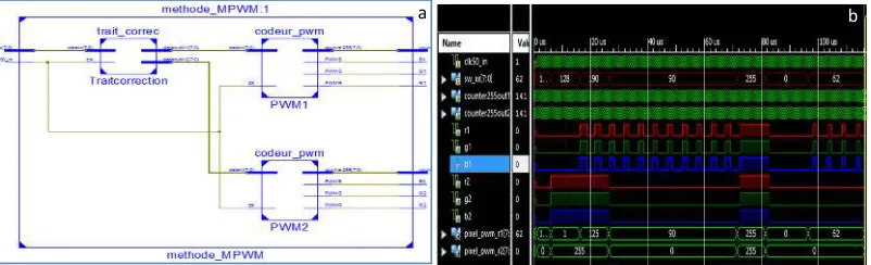
The Fig. 9 shows the data processing and correction block, this block contains two sub-blocks; the first block treats input data using the algorithm explained above then it is separated to two sub-signals pixel_pwm1 and pixel_pwm2. These signals are sent separately to two coders blocks Codeur_PWM. They take the decision and assign different levels to the two outputs signals (r1,g1,b1) and (r2,g2,b2).
Fig. 9 : (a) Block test data processing and correction.(b) Simulation of the block processing test and data correction
Firstly, the block test of improved PWM method was simulated to check behavioral operating. The
Fig.
11
shows behavioral simulation results in the form of timing diagram obtained by the hardware simulation using ISim-HDL of the above processing block, it shows the timing of each main signals. The pixel data signal was presented by input sw_xx (0, 90, 190 and 255), on theFig.
11
when sw_xx equal to 90 signal pixel_pwm1 has same value and signalswitches to input pixel data (0 to 255) and the six fast FX2_IO to generate r1, g1, v1 and r2, g2, v2
outputs to LED. as shown in Fig. 10.
In order to evaluate the output results, we are using oscilloscope to visualize the variation of the output signal according to the value entered by the switches.
.
[image:6.595.99.500.416.538.2]ISSN: 1992-8645 www.jatit.org E-ISSN: 1817-3195
Fig. 10 : Experiment of the control of the luminance intensity
Fig. 11 : oscilloscope visualization (a) for sw_xx=1, (b) for sw_xx=75, (c) for sw_xx=128,
(d) for sw_xx=255,
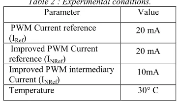
[image:7.595.306.507.308.766.2]Finaly, to evaluate improving efficiency of the color appearance, the pixel’s color intensity of an RGB LED T-1 3/4 (5mm) FULL COLOR LED LAMP of Kingbright Company [15] was used. The luminance intensity values of each RGB component of this LED were measured by using Lux-meter according to the experimental conditions presented in Table 2. This test was repeated for both method PWM and improved PWM currents.
Table 2 : Experimental conditions.
Parameter Value
PWM Current reference (IRef)
20 mA
Improved PWM Current reference (INRef)
20 mA
Improved PWM intermediary Current (INRef)
10mA
Temperature 30° C
The result is depicted on Table 3 as a relationship between the number of the pixel under test, between 0 and 255, for the red, green and blue components and the relative intensity of the luminous.
This experimentally measures were illustrated in Fig. 12 as graphs. Based on the interpolation of the practical results presented in Table 3, these graphs show clearly that the improved PWM
conceptualized curves represented in Fig. 6. As expected by design part, the maximum luminance gain occurs in the intermediate area for all three colors. In general, the improved PWM process generates a higher luminance in same PWM average current conditions. For the PWM method, the linear relationship between duty cycles values and luminous intensity has a constant slope. For the improved PWM method, it contains different linear sections in pieces with differentiated slopes.
According to the practical results, average of the experimental values were calculated and presented in Fig. 13. The graphic shows that the Improved PWM are improve up by 12% for Red color, 10% for Green color and 12% for Blue color.
Table 3 : Experimental results of PWM and improved PWM luminance variations
Data RPW
M RIP WM
GPW M
GIP WM
BPW M
BIP WM
0 0 0 0 0 0 0
25 21 16 49 65 4 5
50 27 43 99 125 7 10
75 49 65 145 180 10 14
100 62 82 175 240 14 19
125 76 98 224 289 18 23
150 81 102 252 311 20 25
175 90 110 300 350 23 28
200 101 118 325 365 25 29
225 110 122 355 380 28 31
250 124 128 370 381 31 32
255 130 131 389 391 32 33
d c
[image:7.595.98.280.549.654.2]ISSN: 1992-8645 www.jatit.org E-ISSN: 1817-3195 Fig. 12 : Variation of the luminance PWM and MPWM
of the R G B LEDs.
Fig. 13 : Experimental average values of each PWM
5. CONCLUSION
In this paper, the principle of driving LED module display was introduced.
The luminous efficiency of this kind of display deserves further exploration in order to improve the overall efficiency of the system.
Conventional luminance variation methods in these displays (PWM methods) were analyzed and discussed in detail.
The proposed solution to improve PWM method was demonstrated mathematically. It was based on approaching PWM curve to DC curve and reducing the error gap between them. The algorithm for this solution method was proposed using less complex hardware with less changing in module driver structure. This makes it suitable for hardware implementation on an FPGA platform. So, an efficient method for converting pixel’s intensity directly to an intensity level of an LED is proposed.
Serial of experiments was realized to check the feasibility of this improved method. Experimental results show that improved PWM can improve the average value by up to 12%, with small addition to the hardware which does not destabilize the operation and structure of the display system. The luminous efficiency according to the DC variation method is always higher than the improved PWM methods. The Improved PWM curve can reach the DC method curve, using more intermediate points but the hardware becomes more complex and must use more driver modules, which influence in energy consumption and cost of system.
REFERENCES :
consumption estimate, USA: U.S. Department of Energy, , September 2002.
[3] V. Abramov, A. Puisha, I. Polyakova, M. Tomilin et A. Chuvashov, «LED modules for large screens,» Journal of Optical Technology, vol. 70, n° %17, p. 492–494, July 2003.
[4] F. Nguyen, «Challenges in the design of a RGB LED display for indoor applications,» Synthetic Metals, vol. 122, n° %11, p. 215–219, May 2001.
[5] Avago, «Introduction to Driving LED Matrices,»
[En ligne]. Available:
http://www.avagotech.com/docs/AV02-3697EN. [Accès le 26 05 2016].
[6] I. H. Oh, «A single-stage power converter for a large screen LCD back-lighting,» chez in
Proceedings of IEEE Applied Power
ElectronicsConference and Exposition, March 2006.
[7] K. H. Loo, Y. M. Lai, S. C. Tan et C. K. Tse, «On the color stability of phosphor-converted white LEDs under dc, PWM, and bilevel drive,» Power
Electronics, IEEE Transactions on, vol. 27,
n° %12, p. 974–984, Feb 2012.
[8] A031E, «PWM vs analog dimming of LED,» Aimtec Inc, 2011.
[9] B. Ackermann, V.Schulz, C.Martiny, A.Hilgers et X.Zhu, «Control of LEDs,» chez in Record of IEEE Industry Applications Conference, October 2006.
[10] M. Xichao et Z. Yuanyue, «Consecutive PWM driving video LED display system,» in:
Proceedings of ISCAS, vol. 97, p. 1437–1439,
1997.
[11] P. Narra et D. S. Zinger, «An effective LED dimming approach,» chez in Record of IEEE Industry Applications Conference, October 2004.
[12] W. Kurdthongmee, «Design and implementation of an FPGA-based multiple colour LED display board,» Microprocessors and Microsystems, vol. 29, p. 327–336, 2005.
[13] C. C. Chen, C. Y. Wu et T. F.Wu, «LED back-light driving system for LCD panels,» chez in
Proceedings of IEEE Applied Power Electronics
Conference and Exposition (APEC), Mars 2006.
[14] ,. Xilinx, «Spartan-3 FPGA Starter Kit Board User Guide,» [En ligne]. Available: www.xilinx.com.. [Accès le 15 03 2016].
[15] KingBright, «Data-sheet LED RGB,» 19 11 2016.
[En ligne]. Available:
![Fig. 4 : Typical LED driver module [13].](https://thumb-us.123doks.com/thumbv2/123dok_us/8907616.957570/4.595.88.506.65.290/fig-typical-led-driver-module.webp)